HAL Id: hal-00867023
https://hal.univ-brest.fr/hal-00867023
Submitted on 27 Sep 2013HAL is a multi-disciplinary open access archive for the deposit and dissemination of sci-entific research documents, whether they are pub-lished or not. The documents may come from teaching and research institutions in France or abroad, or from public or private research centers.
L’archive ouverte pluridisciplinaire HAL, est destinée au dépôt et à la diffusion de documents scientifiques de niveau recherche, publiés ou non, émanant des établissements d’enseignement et de recherche français ou étrangers, des laboratoires publics ou privés.
A 180° tunable analog phase shifter based on a single
all-pass unit cell
Khaled Khoder, André Pérennec, Marc Le Roy
To cite this version:
Khaled Khoder, André Pérennec, Marc Le Roy. A 180° tunable analog phase shifter based on a single all-pass unit cell. Microwave and Optical Technology Letters, Wiley, 2013, 55 (12), pp.2915-2918. �10.1002/mop.27955�. �hal-00867023�
A 180° tunable analog phase shifter based on a
single all-pass unit cell
K. KHoder, A. Pérennec and M. Le Roy
ABSTRACT: This letter describes an analog phase shifter (PS) able to provide a
continuously tunable phase shift up to 180° by using a single all-pass unit cell. The proposed topology is compact and easy to implement, and brings an interesting compromise between phase variation, insertion and return losses. Indeed, for a 7.5:1 tuning ratio of varactor capacitance, a phase shift variation of more than 186° is obtained from 6 to 7 GHz with a maximum insertion loss of 1.8 dB. The 105 °/dB resulting Figure-of-Merit (FoM) is thus among the best in distributed approaches with varactors.
Key words: phase shifters; tunable phase shifter; all-pass network; phase array.
Authors’ affiliations:
K. KHoder, A. Pérennec and M. Le Roy
Lab-STICC (UMR CNRS 6285), Université Européenne de Bretagne (UEB), Université de Bretagne Occidentale (UBO)
6 avenue Le Gorgeu, CS93837, 29238 Brest cedex 3 E-mail : [email protected] ; [email protected] Fax : (33) 2 98 01 63 95
1. INTRODUCTION
Phase shifters (PS) have applications in various microwave radio equipment, for
example in phases array antennas [1]-[2]. PS transfers the appropriate phase values
to the antenna elements in order to form the main beam of electronically-scanned
phased array antennas. As analog phase shifters provide a continuously variable
phase shift, they are likely to meet a wide range of potential applications. Analog PS
specifications are very restrictive, particularly on the phase flatness over the
bandwidth and on the phase shift variation versus the active component tunability. In
many cases, several stages of PS are cascaded to compensate for a restricted range
of variation but at the expense of insertion loss and thus of the final Figure-of-Merit
(FoM). This is particularly true for low-pass and high-pass topologies. Thus, all-pass
circuits are preferably used: e.g. a conventional distributed PS implemented with a
3-dB 90° hybrid branch-line coupler [2]-[3] with two varactors or a more compact
topology with a wider operating frequency range as proposed by Hayashi & al [4].
Both designs are suitable for frequency domain where lumped elements can no more
be used. Compared to these previous works, the topology described in this paper
reaches a new level of compactness and phase-variation range.
2. Circuit configuration
The proposed all-pass PS consists in a coupled-line section connected at one end
(like a Schiffman section) and associated with two varactors C1 and C2 as depicted
in Figure 1. The whole analysis of the novel topology was done by considering the
even and odd mode approach to derive the phase expression as well as the
matching conditions. Optimal input-output matching conditions (S11dB and S22dB
frequency f0. In that case, a simplified relation between the two varactor capacitances
and the even mode impedance is obtained:
2 0 2 1 0 4( ) e Z C C Z (1)
A specific case is obtained from (1) by setting the even-mode impedance Z0e = 50 Ω.
Thus, it corresponds to 50 Ω uncoupled lines of 90° electrical length (i.e. the unfolded
design proposed in [4]) and leads to C2= 4C1 as given by synthesis relation from [4].
In the general case (quarter-wavelength coupled section), choosing an integer ratio
k=C2/C1 will simplify the design with identical varactors in chip package. Setting k=2
corresponds to a medium coupling ratio with
Z
0e
2.
Z
0
70.7
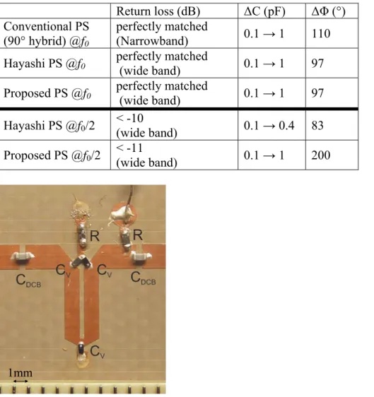
, thus relaxing constrains on technological dimension and sensitivity. In these configurations, i.e.with quarter-wavelength lines at f0 (here 10 GHz), Table 1 compares the phase
variations (∆Φ) at f0 from respectively the conventional PS, the Hayashi's PS and the
proposed PS for an identical varactor tuning range (∆C). Results are close; however
Hayashi and our PS unit cells exhibit a much wider matched frequency band.
Maximizing phase deviation is our main objective; this feature appears around f0/2 (5
GHz) for these latter PSs together with an input/output matching degradation. It
corresponds to an inflexion point in the phase curves and seems promising to get at
least 180° phase agility at the condition that a satisfying level of S11 may be obtained.
In this aim, a multi-criteria optimization on the coupled-line section of the proposed
PS was set under ADS software. At this frequency, optimum even and odd mode
impedances are found to be respectively equal to 92 Ω and 47 Ω (for k=2). The
phase variation is improved up to 200° (Table 1) and the circuit remains matched
over the entire varactor tuning range. On the other hand, the Hayashi unit cell
3. EXPERIMENTAL VALIDATIONS
To highlight the benefits of this topology, a proof-of-concept PS was designed for the
6-7 GHz frequency band. MA46H120 varactor from M/A-COM [5] was used; our
measurements showed that its capacitance value goes from 1.15 to 0.15 pF for a
control voltage varying respectively from 0 to 15 V. These values are in overall
agreement with those provided by the manufacturer. The varactor measured
S-parameters and EM models for the distributed microstrip sections were taken into
account in the final optimization process, together with bias component influence.
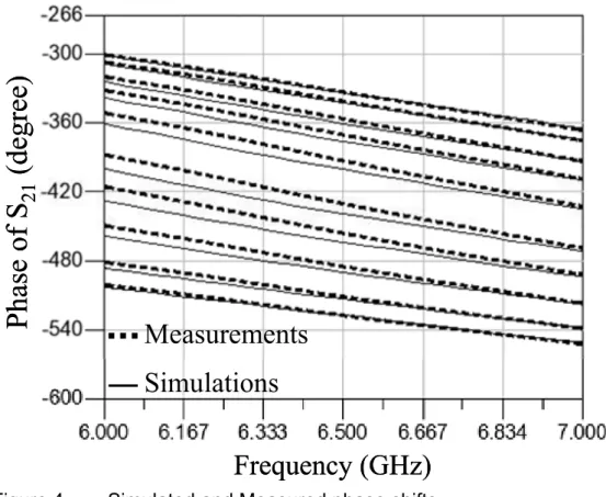
Figure 2 shows a photograph of the constructed PS on an RF-35 substrate
(h = 0.78mm, r = 3.5, tan δ = 0.0023) and all the lumped components used. CDCB are
the DC blocking capacitors; resistances, R, are used to bias the varactors, CV. Two
varactors of capacitance CV were placed in series to get C1 = CV/2, and another one
was connected to the ground plane to get C2 = CV. Thus, only a single bias point is
required.
Figure 3 shows the simulated and measured results of S11 and S21 magnitudes: a
good agreement is obtained. Bias voltage was varied from 0 to 15 V. From the
measured results, it can be seen that the circuit is well matched in a wide frequency
band, which verifies it all-pass behaviour. Minimum phase error and a good insertion
loss are obtained in the 6–7 GHz. In this band, the maximum insertion loss is 1.8 dB
and the return loss is better than 12 dB.
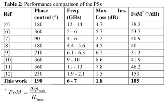
In Figure 4, the comparison between the simulated and measured phase shift shows
a good agreement. For just one cell, the phase shift can be tuned by more than 180°
over the entire bandwidth.
The error on the phase is lower than ±8° for all over the entire voltage span. Table 2
phase shifters with varactors. To our knowledge, the proposed phase shifter has the
best compromise between FoM and bandwidth among the reported phase shifters.
4. CONCLUSION
In this letter, we have presented a novel topology of PS designed using distributed
components and varactors. We have shown the benefits of this topology compared to
similar existing approaches. The proposed PS was optimized to ensure matching for
the 6-7 GHz operating frequency range and to provide a wide phase-agility range
with low phase error. In this whole band, a single unit-cell PS allows a continuously
tunable phase shift of more than 180° with only one control voltage. Although it is
implemented in hybrid technology, the circuit is compact with a low insertion loss;
References
1 D. M. Pozar, and D. H. Schaubert, Comparison of architectures for monolithic phased array antennas, Microwave J. (1986), 93–104
2 D. M. Pozar, Microwave Engineering, John Wiley and Sons, Inc., (1998), sections 9-10.
3 N. Gupta, R. Tomar, and P. Bhartia, A Low-loss voltage-controlled analog phase-shifter using branchline coupler and varactor diodes, Int. Conf. Microw. Millimeter Wave Tech., (2007), 1-2.
4 H. Hayashi, T. Nakagawa, and K. Araki, A Miniaturized MMIC Analog Phase Shifter Using Two Quarter-Wave-Lengh Transmission Lines, IEEE Trans. Microw. Theory Tech., 50, (2002), 150-154.
5 MA46H120 series, GaAs constant gamma Flip-chip Varactor diode, http://www.macomtech.com/datasheets/MA46H120.pdf, MA-COM
6 F. Ellinger, H. Jäckel, and W. Bächtold, Varactor-loaded transmission-line phase shifter at C-band using lumped elements, IEEE Trans. Microw. Theory Tech., 51, (2003), 1135-1140.
7 F. Ellinger, R. Vogt, and W. Bächtold, Ultra compact, low loss, varactor tuned phase shifter MMIC at C-band, IEEE Microw. Wireless Comp. Lett., 11, (2001), 104–105
8 K. Hongjoom, B.K. Alexander, K. Abdolreza, and D. W. van der Weide, Linear Tunable Phase Shifter Using a Left-Handed Transmission Line, IEEE Microw. Wireless Comp. Lett., 15, (2005), 366-368.
9 F. Ellinger, R. Vogt, and W. Bächtold, Compact reflective type phase shifter MMIC for C-band using a lumped element coupler, IEEE Trans. Microw. Theory Tech., 49, (2001), 913-917.
10 D. Shin, G. M. Rebeiz, Low-power low-noise 0.13 m CMOS X-band phased array receivers, IEEE, Int. Microw. Symp. Digest, (2010), 956–959. 11 L. Wei-Tsung, K. Yen-Hung, W. Yi-Ming, and T. Jeng-Han, An X-band
full-360° reflection type phase shifter with low insertion loss, Proceedings of the 7th European Microw. Integrated circuits Conf., (2012), 754–757. 12 S. M. Han, C. S. Kim, D. Ahn, and T. Itoh, Phase shifter with high phase
shifts using defected ground structures, Electron. Lett., 41, (2005), 196-197.
Figure captions
Z
0o, Z
0e Z0 Z0C
2L
Input port Output portC
1Z
0o, Z
0e Z0 Z0C
2L
Input port Output portC
1Z
0o, Z
0e Z0 Z0C
2L
Input port Output portC
1Figure 1 Proposed all-pass phase shifter topology
Table 1: Comparison of maximum phase variation (ΔΦ) and matching for a capacitance
variation (ΔC) for conventional, Hayashi and proposed PSs
Return loss (dB) ΔC (pF) ΔΦ (°) Conventional PS (90° hybrid) @f0 perfectly matched (Narrowband) 0.1 → 1 110 Hayashi PS @f0 perfectly matched (wide band) 0.1 → 1 97 Proposed PS @f0 perfectly matched (wide band) 0.1 → 1 97 Hayashi PS @f0/2 < -10 (wide band) 0.1 → 0.4 83
Proposed PS @f0/2 < -11 (wide band) 0.1 → 1 200
Figure 2 Phase shifter photograph. CDCB = 47 pF, R = 3.3 kΩ, CV are MA46H120
varactors, line width W=1.07 mm and slot between coupled lines, S= 0.31 mm
1mm 1mm
Figure 3 (a) Simulated and (b) Measured S-Parameters
Measurements
Simulations
Frequency (GHz)
Ph
ase of
S
21(degre
e)
Measurements
Simulations
Measurements
Simulations
Frequency (GHz)
Ph
ase of
S
21(degre
e)
Figure 4 Simulated and Measured phase shifts (a) Frequency Simulation S2 (dB) S1 (dB Frequency (a) S2 (dB) S1 (dB Frequency (GHz) Measurements S21(dB S11(dB Frequency (GHz) (b) S21(dB S11(dB
Table 2: Performance comparison of the PSs Ref Phase control (°) Freq. (GHz) Max. Ins. Loss (dB) FoM * (°/dB) [4] 180 12 - 14 4.7 38.2 [6] 360 5 - 6 5.7 53.7 [7] 90 4 - 6 2.2 40.9 [8] 180 4.4 - 5.6 4.5 40 [9] 210 6.1 - 6.3 6.7 31.3 [10] 360 9 - 10 8.6 41.9 [11] 360 11 - 13 7.8 46.2 [12] 230 1.9 - 2.1 1.5 153 This work 190 6 - 7 1.8 105 * max max