an author's https://oatao.univ-toulouse.fr/21794
http://dx.doi.org/10.1109/TED.2014.2323997
Marcelot, Olivier and Maximenko, Sergey and Magnan, Pierre Plan View and Cross-Section View EBIC
Measurements: Effect of e-Beam Injection Conditions on Extracted Minority Carrier Transport Properties. (2014) IEEE Transactions on Electron Devices, 61 (7). 2437-2442. ISSN 0018-9383
Abstract—Application of low doped epitaxial layers and the increase of complexity of silicon photodiode design require the knowledge of the basic physical parameters such as minority carrier lifetime or diffusion length in order to improve the photodiode performance simulation. In this paper, EBIC technique is used to evaluate minority carrier lifetime and diffusion length on a silicon photodiode. Particular focus is to compare plan view and cross-section view testing geometry, and also to evaluate artefacts introduced by high injection conditions unavoidable in lifetime measurement.
Index Terms— scanning electron microscopy (SEM), electron beam induced current (EBIC), semiconductor materials measurements.
I. INTRODUCTION
he increased performance in terms of quantum efficiency and long wavelength compatibility of modern CMOS image sensors require the use of low-doped epitaxy material [1], [2], [3], and more complex photodiode design [4], [5]. The device quantum efficiency response is strongly affected by the minority carrier transport properties in the low doped absorber area. Therefore, it is crucial to precisely determine basic physical parameters (minority diffusion length (L), lifetime ()) in order to improve the simulations of these devices.
The Electron Beam Induced Current (EBIC) mode of scanning electron microscopy (SEM) is a widely used technique to characterize semiconductor materials and devices. Among all the available applications, it allows the evaluation of the minority carrier diffusion length [6], [7], [8], [9] and the minority carrier lifetime [10], [11].
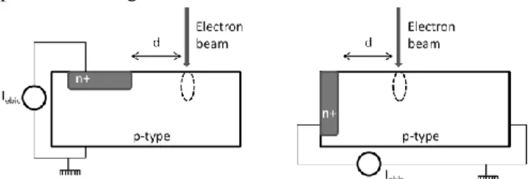
Generally, EBIC diffusion length and transient lifetime measurements are performed in the cross sectional or plan view geometry as shown in Fig. 1. The preparation of the sample for cross-sectional measurements alters the surface quality, which can influence measurements. In addition, injection level conditions are important factors to consider.
O. Marcelot (e-mail: [email protected]), P. Magnan (e-mail:
[email protected]) are with ISAE, Université de Toulouse, Image Sensor Research Team, 10 avenue E.Belin, F-31055, Toulouse, France.
S. Maximenko is with Naval Research Laboratory, Washington, D.C. 20375, USA (e-mail: [email protected]).
Diffusion length or lifetime of minority carriers should be extracted from EBIC measurement under low injection conditions [8], [11], [12], [13], i.e. such that the excess minority-carrier density is much lower than the equilibrium majority-carrier density. However, in particular lifetime measurements demand a wideband and low noise amplifier, which generally does not offer a high gain. Therefore, a high beam current is used to be compatible with the amplifier and the experiment usually is done at high excitation. In some cases, when the device geometry allows for it, the defocusing of e-beam could override this problem.
In spite a great number of publications on the use of the EBIC technique for extraction of the minority carrier diffusion length, it is not straightforward, which injection level range and testing configuration suites the best to get most reliable results. In this paper it is attempt to compare generally used cross sectional and plan view geometries and evaluate the impact of the injection level conditions on the diffusion length and the lifetime measurements. The theory of diffusion length and lifetime EBIC measurement is presented as background for interpretation of the experimental results.
The application of EBIC technique for characterization of the minority carrier diffusion length has been intensively studied, in terms of analytical approach and experimental analysis [7], [8], [12], [14], [15]. Two widely applied geometries for extraction of L from EBIC line scan are presented in Fig. 1.
The interaction of the electron beam with the semiconductor substrate creates electron-hole pairs at the distance d from the edge of the space charge region. Some of the minority carriers diffuse and are collected by the junction, and give rise to a current. This current collected by Ohmic contacts is measured by a current amplifier. The recorded current profile has a peak maximum at the position of the junction with further decay as
Plan View and Cross-Section View EBIC
Measurements: Effect of e-Beam Injection
Conditions on Extracted Minority Carrier
Transport Properties.
O. Marcelot, S. Maximenko, P. Magnan
T
Fig. 1. Experimental set-up for EBIC characterization. On the left side plan view configuration, and on the right side cross-section configuration.
e-beam moves away due to bulk and surface recombination and described by [9], [15]:
L
d
d
A
I
EBIC nexp
(1)where A is a constant, and L the carrier minority diffusion length. The “n” factor depends on the surface recombination (s) and scan geometry. Thus, in the cross sectional geometry it varies between 0 (s=0) and 0.5 (s=∞), while in plan view n has a range between 1/2 (s=0) and 3/2 (s=∞) [16]. Then the diffusion length can be extracted from the slope of ln(IEBICd
n
) as function of the distance (d). As the surface recombination s is usually an unknown parameter, n is adjusted to get a straight line. It should be noted that the starting point to fit data should be at least two diffusion lengths from the junction and also more than the lateral dimension of the generation volume such that no generation of e-h pairs in depletion region occurs.
Analytical expression for EBIC current in cross-section configuration is given by [7], [14], [15], [17], [18]. In this work the Donolato’s approach, which includes the extended generation by taking a Gaussian source, is adopted to simulate EBIC profile and compare with experimental results. The Donolato’s expression is quite convenient and can be written as a Fourier sine transform of a function containing elementary functions only as shown in equation 2 [7]. However, it is only valid for distances from the junction greater than the lateral extension of the generation volume:
0 0 2 2 2 2 2 02
57
0
2
2
z
exp
.
k
exp
k
d
I
EBIC
kx
dk
sin
z
erfc
s
s
0 2 02
(2)where z0 and σ are parameters related to the electron range, R,
defined as [7]:
R
.
z
0
0
3
;15
R
(3) and µ and λ areL
1
;
k
2
2 (4) The electron range R is defined by the expression given by [19].Another way to evaluate transport properties of minority carriers is analyzing transient EBIC signals in the structure induced by high-speed chopped e-beam [11], [17], [20]. The extraction of the minority carrier lifetime can be performed from equation (5) proposed by Ioannou [11].
12
A
exp
t
t
t
I
EBIC (5)where A is a constant, and τ the minority carrier lifetime. Then, the lifetime is simply extracted from the slope of straight line given by
ln
I
t
.II. EXPERIMENTAL DETAILS
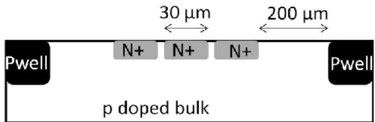
A photodiode matrix consisting of 12 30x30 µm n+-p individual devices fabricated on a p-type (1x10¹⁵ B.cm-3) silicon bulk substrate and passivated by a silicon oxide layer with a thickness of 6 m and surrounded by a Pwell guard ring (Fig. 2) was used in experiment. The device structure was manufactured using deep submicron CMOS imaging technology [21]. The top oxide layer was thinned down to ~1
m to access plan view EBIC measurements.
In addition, a part of the diode matrix was cut off by a diamond saw and polished with SiC sandpaper and an alumina colloidal solution (0.1 µm) to conduct cross-sectional EBIC measurements. A Keithley 428 current amplifier plugged to the SEM video input was used to visualize EBIC signal (Fig. 3). While slow EBIC line scans (25 mHz) were analyzed using Keithley 6514 electrometer, transient signals amplified by a Femto HCA-200M-20K-C with a bandwidth of 200 MHz and a trans-impedance gain of 20000 2x10⁴ V/A were monitored by digital oscilloscope, triggered by the SEM electromagnetic beam blanker. All measurements were performed with a 30 kV beam accelerating voltage, which corresponds to an e-beam penetration depth of 7 µm [9], and absorbed e-beam current in the range of 4 pA – 20 nA at FEI Inspect S-50 SEM equipped with a tungsten filament. The beam current was monitored using Faraday cap mounted on stage.
Fig. 3. Composed SE/EBIC images of (a) the cross cut and (b) front view the photodiode matrix captured at 30 keV accelerating voltage.
III. DIFFUSION LENGTH MEASUREMENTS
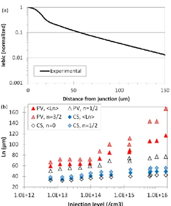
Figure 4 shows normalized experimental cross-sectional profiles obtained with a 17 pA beam current together with simulated ones for the same excitation conditions using equation 2. As can be seen, the shape of the simulated scan is strongly influenced by the surface recombination (s) and diffusion length (L) values. The best fit to the experimental scan is obtained using s=4x105 cm/s, which is in good agreement to values reported by other researchers for Si [15], [18], and L=50 µm. The experimental values of diffusion length found from eq. 1 are in the range of 32.3 µm < Ln < 40 µm (n=0-1/2) with average L=36 µm which is close to simulated one. Further in the article all diffusion length values will be extracted using Chan and Schroder approach (eq. 1) [15].
The L results for variable e-beam current values at the same accelerating voltage of 30 kV are presented in Fig. 5. The corresponding maximum injection level of e-beam in the center of the electron-hole generation volume can be estimated as [22]:
L
b
exp
L
b
D
L
b
G
n1
1
4
3
2 3 (6)where G is the generation rate, b=1/2R the radius of the
uniform generation sphere, R [19] the electron range, L the diffusion length and D the diffusion constant of the minority carrier. As can be seen, the minority carrier diffusion length is quite stable up to 17 pA beam current (injection level: 2.6x1013cm-3), which is ~0.05 times the base doping (1.0x1015cm-3), with further gradual increase for higher injection levels. This finding correlates with results published by other researchers [12], [23].
The diffusion length reaches a maximum value at the injection level within an order of magnitude of the base doping. It was shown that the minority carrier lifetime and diffusion length could be increased at high injection level, because of enhanced density of ionized centers [12], [24]. It should be mentioned that the diffusion length range for extreme boundary conditions (n=0, 1/2) significantly increases for high-level injection conditions. This illustrates the importance of the controlling of the injection level conditions during experiment.
An example of the EBIC line scan profile captured in plan view geometry at an e-beam current of 15 pA (injection level: 2.4x1013cm-3) is presented in Fig. 6(a). By analyzing the EBIC linescan signal the average diffusion length extracted from the slope of the line ln(IEBICdn) has value of 63 µm. Comparison of
L values extracted in cross-section and in plan view geometry for various beam current is summarized in Fig. 6(b). Diffusion length results obtained in plan view geometry show higher values in comparison to measurements performed in cross-section view.
Fig. 5. Experimental values of L for extreme boundary conditions (n=0, 1/2) and their average values extracted at variable injection levels and accelerating voltage 30 keV.
Fig. 4. Experimental EBIC linescan captured at 17 pA beam current and E=30kV along with simulated profiles (a) for L=50 µm and various surface recombination velocities s, and (b) for s=4x10⁵ and various minority
Overall, the average diffusion lengths measured in plan view exceed by minimum 20 µm the cross-section L results at the same excitation conditions. It can be explained by the absence of a roughly cut surface and by the presence on the surface of an oxide passivation layer, which reduces the surface recombination velocity in the plan view testing geometry.
In order to evaluate the impact of the surface recombination for cross-sectional testing geometry, the diffusion length was extracted for different penetration ranges of the e-beam (from 5 keV to 30 keV) as shown in Fig. 7. A strong decrease of L at small accelerating voltages is attributed to enhanced effect of the surface recombination. Consequently, minority carrier
diffusion length should be extracted in plan view geometry with an injection level lower than 0.05 times the substrate doping.
IV. LIFETIME MEASUREMENTS
The experiment is performed on the same photodiode in cross section with a beam current of 6 nA (injection level of 9.5x1015 cm-3) and 11.6 nA (injection level of 1.8x1016 cm-3), which correlates to a high injection condition. Low signal to noise ratio at lower injection conditions limited the use of low e-beam currents. As an example, the captured EBIC signal at 9.5x1015 cm-3 injection level is shown in Fig. 8. Even at high injection level the raw EBIC decay signal is quite noisy.
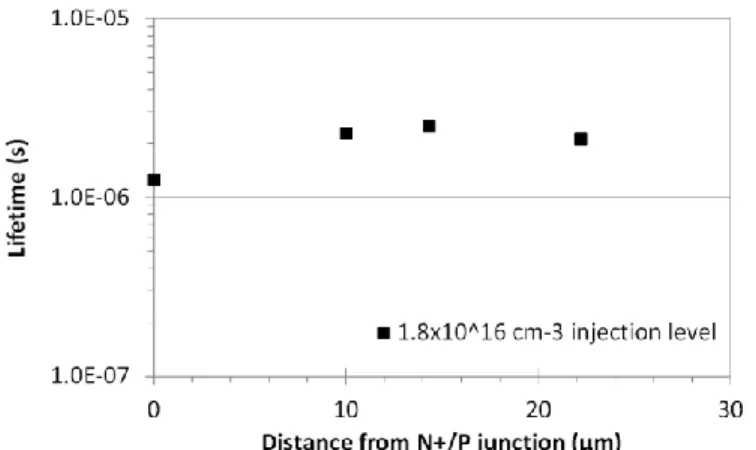
Lifetime extractions are performed at different depth from the n+-p junction, and results are reported in the Fig. 9.
For both beam currents, the lifetime measured on the junction position is shorter, because of the higher dopant concentration of the junction. All other points are homogenous and give a lifetime of 1.5 µs for the highest beam current, and 2 µs for the lowest beam current.
The minority carrier diffusion length and the lifetime are Fig. 9. Experimental values of the effective lifetime from analysis of transient EBIC in cross section geometry as position from the edge of p-n junction.
Fig. 8. Experimental profile of transient EBIC performed with a 1.8x1016 cm -3 injection level, and smoothed profile.
Fig. 7. Average (<Ln>) minority carrier diffusion length as function of e-beam penetration depth at injection level 1.0x1014.cm-3 (cross-section
geometry).
Fig. 6. (a) Experimental plan view line scan EBIC profile and (b) experimental measurement of average (<Ln>) for extreme n values minority carrier diffusion length for variable injection levels at 30 keV in plan view and in cross-section geometry.
linked by the following relationship:
n n
n
D
L
(7) At the high injection level, the diffusion coefficient and the mobility decrease as the injected carrier concentration increases [25], [26]. In a substrate doped at 1015 B.cm-3, the mobility should decrease from 1400 cm²V-1s-1 (low injection) to 1000 cm²V-1s-1 (high injection), and thus the diffusion constant should decrease from Dnlo=35 cm²s-1 to Dnhi=25 cm²s -1. Then, let us make the approximation Lnhi≈1.37Lnlo; using
equation 7 for low and high injection it comes:
nhi nlo nhi nhi nlo
.
D
.
D
0
38
37
1
2 (8)where τnhi is the measured lifetime in high injection
condition, Dnhi the diffusion constant at high injection level,
and Dnlo the diffusion constant at low injection level.
Consequently, the carrier lifetimes measured at high injection level can be overestimated by a factor of 2.6. The corresponding estimated carrier lifetimes which can be measured at low injection condition are estimated: 0.57 µs for the highest beam current and 0.76 µs for the lowest beam current. These values of carrier lifetime are consistent with those which could be deduced from diffusion length measurements. Indeed, taking into account a diffusion constant for minority carriers Dn of 35 cm²/s [25], Ln=50 µm
gives τn=0.7 µs (injection level of 2.6x1013 cm-3).
Following the same approach, the lifetime was evaluated in plan view geometry at different distance from the n+ cathode to increase the statistic, and to check the results consistency. Results are shown in the Fig. 10. However, due to the presence of thick oxide layer on the surface, the measurements are more challenging, and require higher injection level conditions to get acceptable signal to noise level.
The measured lifetimes are showing an average minority carrier lifetime of around 2 µs, which is slightly longer than that of the cross-section measurement. Therefore, in spite of a
challenging experimental set-up, we have shown that it is possible to evaluate the minority carrier lifetime in plan view, without any specific sample preparation. The experimental configuration could be improved, in particular by thinning down the oxide stack in the electron beam incidence zone.
V. CONCLUSION
Measurement of the minority carrier diffusion length and lifetime is performed on a photodiode processed on a silicon bulk p doped wafer, using both a plan view and a cross-section configuration. For all e-beam excitation level conditions, diffusion lengths values in plan view testing geometry consistently have longer diffusion lengths than those measured in cross section, which is related to the impact of surface recombination. In addition, it was found that injection level conditions have a strong influence on the extracted diffusion length values. Particularly, similar L values were obtained for excitation levels up to ~0.05 times of the substrate doping with following gradual increase for higher injection levels. An evaluation of the minority carrier properties from transient EBIC measurements can represent significant difficulty and prone to be conducted at high injection level condition to maintain high signal to noise ratio, which leads to over evaluation of the extracted lifetime values. Particularly, for the structure reported in the paper it was found that the minority lifetime is over evaluated by ~2.6 times. This should be kept in mind while choosing the EBIC testing setup and injection conditions.
REFERENCES
[1] S.E. Holland, D.E. Groom, N.P. Palaio, R.J. Stover, M. Wei, “Fully-Depleted, Back-Illuminated Charge-Coupled Devices Fabricated on High-Resistivity Silicon,” IEEE Trans. Electron Devices, vol. 50, no. 1, pp. 101-114, Jan. 2003
[2] W. Dulinski, A. Braem, M. Caccia, G. Claus, G. Deptuch, D. Grandjean, C. Joram, J. Seguinot, M. Winter, “Tests of a backside illuminated monolithic CMOS pixel sensor in an HPD set-up,” Nucl. Instr. and Meth. A, vol. 546, pp. 274-280, 2005
[3] W. Snoeys, J.D. Plummer, S. Parker, C. Kenney, “PIN Detector Arrays and Integrated Readout Circuitry on High-Resistivity Float-Zone Silicon,” IEEE Trans. Electron Devices, vol. 41, no. 6, pp. 903-912, Jun. 1994
[4] A.J.P. Theuwissen, “CMOS image sensors: State-of-the-art,” Solid St. Electron., vol. 52, pp. 1401-1406, 2008.
[5] P. Lee, R. Gee, M. Guidash, T. Lee, and E. R. Fossum, “An active pixel sensor fabricated using CMOS/CCD process technology,” in Proc. IEEE Workshop on CCDs and Advanced Image Sensors, 1995, pp. 115–119 [6] W. H. Hackett, Jr., R. H. Saul, R. W. Dixon, and G. W. Kammlott,
“Scanning electron microscope characterization of GaP red-emitting diodes,” J. Appl. Phys., vol. 43, pp. 2857-2868,1972
[7] C. Donolato, “On the Analysis of Diffusion Length Measurements by SEM,” Solid St. Electron., vol. 25, no. 11, pp. 1077-1081, 1982. [8] D.E. Ioannou, C.A Dimitriadis, “A SEM-EBIC Minority-Carrier
Diffusion-Length Measurement Technique,” IEEE Trans. Electron Devices, vol. ED-29, no. 3, pp. 445-450, Mar. 1982
[9] D. K. Schroder, “Semiconductor Material and Device Characterization”, 2nd ed., Wiley-Interscience, New York (1998).
[10] M. Watanabe, G. Actor, H.C. Gatos, “Determination of Minority-Carrier Lifetime and Surface Recombination Velocity with High Spacial Resolution,” IEEE Trans. Electron Devices, vol. ED-24, no. 9, pp. 1172-1177, Sep. 1977
Fig. 10. Effective lifetime extracted in plan view configuration for different distances from the junction.
[11] D.E. Ioannou, “A SEM-EBIC minority-carrier lifetime-measurement technique,” J. Phys. D: Appl. Phys., vol. 13, no. 3, pp. 611-617, 1980 [12] D.K. Schroder, “Carrier Lifetimes in Silicon,” IEEE Trans. Electron
Devices, vol. 44, no. 1, p p. 160-170, Jan. 1997
[13] P. B. Klein, “Carrier lifetime measurement in n− 4H-SiC epilayers”, J. Appl. Phys., vol. 103, pp. 033702, Feb. 2008
[14] J.M. Bonard, J.D. Ganiere, “Quantitative analysis of electron-beam-induced current profiles across p –n junctions in GaAs/Al0.4Ga0.6As heterostructures”, J. Appl. Phys., vol. 79, no. 1, pp. 6987-6994, May 1996
[15] D.SH. Chan, V.K.S. Ong, J.C.H. Phang, “A Direct Method for the Extraction of Diffusion Length and Surface Recombination Velocity from an EBIC Line Scan: Planar Junction Configuration,” IEEE Trans. Electron Devices, vol. 42, no. 5, pp. 963-968, May. 1995
[16] O. Kurniawan, V. K. S. Ong, “Generalized EBIC method for extracting diffusion lengths from non-conventional collector structure”, in Proc. Optoelectronic and Microelectronic Materials and Devices, pp. 113-116, 2006
[17] F. Berz, H. K. Kuiken, “Theory of life time measurements with the scanning electron microscope: Steady state,” Solid St. Electron., vol. 19, pp. 437-445, 1976
[18] K.L. Luke, O. Roos, L. Cheng, “Quantification of the effects of generation volume, surface recombination velocity, and diffusion length on the electron beam induced current and its derivative: Determination of diffusion lengths in the low micron and submicron ranges”, J. Appl. Phys., vol. 57, no. 6, pp. 1978-1984, 1985
[19] H.J. Leamy, “Charge Collection Scanning Electron Microscopy”, J. Appl. Phys., vol. 53, no. 6, pp. R51-R80, Jun 1982
[20] T. Kushida, S. Tanaka, C. Morita, T. Tanji, Y. Ohsita, “Mapping of minority carrier lifetime distributions in multicrystalline silicon using transient electron beam induced current”, J. Electron Microsc., vol. 61, no. 5, pp. 293-298, 2012
[21] E. R. Fossum, “CMOS image sensors: Electronic camera-on-a-chip”, IEEE Trans. Electron Devices, vol. 44, no. 10, pp. 1689–1698, Oct. 1997
[22] H. Alexander, “What information on extended defects do we obtain from beam injection methods?”, Mat. Sci. Eng., vol B24, pp. 1-7, 1994 [23] D. Cavalcoli, A. Cavallini, “Evaluation of Diffusion Length at Different
Excess Carrier Concentrations,” Mat Sci Eng B-Solid, vol. 24, no. 1, pp. 98–100, May 1994
[24] D. Bielle-Daspet, F. Espioussas, A. Johan, M. Roux, “High injection effects on conductivity and carrier lifetime in P-type silicon material,” Revue Phys. Appl., vol. 15, pp. 945-959, 1980
[25] S. M. Sze, “Physics of Semiconductor Devices”, 2nd ed. New York: Wiley, 1981
[26] B. Jayant Baliga, “Fundamentals of Power Semiconductor Devices”, Springer Science, 2008