HAL Id: tel-01235370
https://tel.archives-ouvertes.fr/tel-01235370v2
Submitted on 3 Mar 2016
HAL is a multi-disciplinary open access
archive for the deposit and dissemination of sci-entific research documents, whether they are pub-lished or not. The documents may come from teaching and research institutions in France or abroad, or from public or private research centers.
L’archive ouverte pluridisciplinaire HAL, est destinée au dépôt et à la diffusion de documents scientifiques de niveau recherche, publiés ou non, émanant des établissements d’enseignement et de recherche français ou étrangers, des laboratoires publics ou privés.
ware Architecture [cs.AR]. Université Rennes 1, 2015. English. �NNT : 2015REN1S070�. �tel-01235370v2�
THÈSE / UNIVERSITÉ DE RENNES 1
sous le sceau de l’Université Européenne de Bretagne
pour le grade de
DOCTEUR DE L’UNIVERSITÉ DE RENNES 1
Mention : Informatique
École doctorale Matisse
présentée par
Arthur P
ERAIS
préparée à l’unité de recherche INRIA
Institut National de Recherche en Informatique et
Automatique – Université de Rennes 1
Increasing the
Per-formance of
Super-scalar Processors
through Value
Pre-diction
Thèse soutenue à Rennes
le 24 septembre 2015
devant le jury composé de :
Christophe W
OLINSKIProfesseur à l’Université de Rennes 1 / Président
Frédéric P
ÉTROTProfesseur à l’ENSIMAG, Institut Polytechnique de Grenoble / Rapporteur
Pierre B
OULETProfesseur à l’Université de Lille 1 / Rapporteur
Christine R
OCHANGEProfesseur à l’Université de Toulouse/ Examinatrice
Pierre M
ICHAUDChargé de Recherche à l’INRIA Rennes – Bretagne Atlantique /Examinateur
André S
EZNECDirecteur de recherche à l’INRIA Rennes – Bretagne Atlantique /Directeur de thèse
Je tiens à remercier les membres de mon jury pour avoir jugé les travaux réalisés durant cette thèse, ainsi que pour leurs remarques et questions.
En particulier, je remercie Christophe Wolinski, Professeur à l’Université de Rennes 1, qui m’a fait l’honneur de présider ledit jury. Je remercie aussi Frédéric Pétrot, Professeur à l’ENSIMAG, et Pierre Boulet, Professeur à l’Université de Lille 1, d’avoir bien voulu accepter la charge de rapporteur. Je remercie finalement Christine Rochange, Professeur à l’Université de Toulouse et Pierre Michaud, Chargé de Recherche à l’INRIA Bretagne Atlantique, d’avoir accepté de juger ce travail.
Je souhaite aussi remercier tout particulièrement Yannakis Sazeides, Pro-fesseur à l’Université de Chypre. Tout d’abord pour avoir accepté de siéger dans le jury en tant que membre invité, mais aussi pour avoir participé à l’établissement des fondements du domaine sur lequel mes travaux de thèse se penchent.
Je tiens à remercier André Seznec pour avoir assuré la direction et le bon déroulement de cette thèse. Je lui suis particulièrement reconnaissant d’avoir transmis sa vision de la recherche ainsi que son savoir avec moi. J’ose espérer que toutes ces heures passées à tolérer mon ignorance auront au moins été divertis-santes pour lui.
Je veux remercier les membres de l’équipe ALF pour toutes les discussions sérieuses et moins sérieuses qui auront sûrement influencées la rédaction de ce document.
Mes remerciements s’adressent aussi aux membres de ma famille, auxquels j’espère avoir pû fournir une idée plus ou moins claire de la teneur de mes travaux de thèse au cours des années. Ce document n’aurait jamais pû voir le jour sans leur participation active à un moment ou à un autre.
Je suis reconnaissant à mes amis, que ce soit ceux avec lesquels j’ai pû quo-tidiennement partager les joies du doctorat, ou ceux qui ont eu le bonheur de choisir une autre activité.1
Finalement, un merci tout particulier à ma relectrice attitrée, sans laquelle de nombreuses fôtes subsisteraient dans ce manuscrit. Grâce à elle, la rédaction de
Table of Contents 2
Résumé en français 9
Introduction 15
1 The Architecture of a Modern General Purpose Processor 23
1.1 Instruction Set – Software Interface . . . 23
1.1.1 Instruction Format . . . 24
1.1.2 Architectural State . . . 24
1.2 Simple Pipelining . . . 25
1.2.1 Different Stages for Different Tasks . . . 27
1.2.1.1 Instruction Fetch – IF . . . 27 1.2.1.2 Instruction Decode – ID . . . 27 1.2.1.3 Execute – EX . . . 27 1.2.1.4 Memory – MEM . . . 28 1.2.1.5 Writeback – WB . . . 30 1.2.2 Limitations . . . 30 1.3 Advanced Pipelining . . . 32 1.3.1 Branch Prediction . . . 32 1.3.2 Superscalar Execution . . . 33 1.3.3 Out-of-Order Execution . . . 34 1.3.3.1 Key Idea . . . 34 1.3.3.2 Register Renaming . . . 35
1.3.3.3 In-order Dispatch and Commit . . . 37
1.3.3.4 Out-of-Order Issue, Execute and Writeback . . . 39
1.3.3.5 The Particular Case of Memory Instructions . . . 42
1.3.3.6 Summary and Limitations . . . 46
2 Value Prediction as a Way to Improve Sequential Performance 49 2.1 Hardware Prediction Algorithms . . . 50
2.1.1 Computational Prediction . . . 50 3
2.2 Speculative Window . . . 61 2.3 Confidence Estimation . . . 63 2.4 Validation . . . 64 2.5 Recovery . . . 64 2.5.1 Refetch . . . 65 2.5.2 Replay . . . 66 2.5.3 Summary . . . 67
2.6 Revisiting Value Prediction . . . 67
3 Revisiting Value Prediction in a Contemporary Context 69 3.1 Introduction . . . 69
3.2 Motivations . . . 70
3.2.1 Misprediction Recovery . . . 70
3.2.1.1 Value Misprediction Scenarios . . . 71
3.2.1.2 Balancing Accuracy and Coverage . . . 72
3.2.2 Back-to-back Prediction . . . 73
3.2.2.1 LVP . . . 74
3.2.2.2 Stride . . . 74
3.2.2.3 Finite Context Method . . . 74
3.2.2.4 Summary . . . 75
3.3 Commit Time Validation and Hardware Implications on the Out-of-Order Engine . . . 76
3.4 Maximizing Value Predictor Accuracy Through Confidence . . . . 77
3.5 Using TAgged GEometric Predictors to Predict Values . . . 78
3.5.1 The Value TAgged GEometric Predictor . . . 78
3.5.2 The Differential VTAGE Predictor . . . 80
3.6 Evaluation Methodology . . . 81
3.6.1 Value Predictors . . . 81
3.6.1.1 Single Scheme Predictors . . . 81
3.6.1.2 Hybrid Predictors . . . 83
3.6.2 Simulator . . . 83
3.6.2.1 Value Predictor Operation . . . 84
3.6.3 Benchmark Suite . . . 86
3.7 Simulation Results . . . 86
3.7.1 General Trends . . . 86
3.7.1.1 Forward Probabilistic Counters . . . 86
3.7.1.2 Pipeline Squashing vs. selective replay . . . 88
3.7.1.3 Prediction Coverage and Performance . . . 89
3.7.2 Hybrid predictors . . . 90
3.8 Conclusion . . . 92
4 A New Execution Model Leveraging Value Prediction: EOLE 95 4.1 Introduction & Motivations . . . 95
4.2 Related Work on Complexity-Effective Architectures . . . 97
4.2.1 Alternative Pipeline Design . . . 97
4.2.2 Optimizing Existing Structures . . . 98
4.3 {Early | Out-of-order | Late} Execution: EOLE . . . 99
4.3.1 Enabling EOLE Using Value Prediction . . . 99
4.3.2 Early Execution Hardware . . . 101
4.3.3 Late Execution Hardware . . . 102
4.3.4 Potential OoO Engine Offload . . . 105
4.4 Evaluation Methodology . . . 106
4.4.1 Simulator . . . 106
4.4.1.1 Value Predictor Operation . . . 107
4.4.2 Benchmark Suite . . . 108
4.5 Experimental Results . . . 108
4.5.1 Performance of Value Prediction . . . 108
4.5.2 Impact of Reducing the Issue Width . . . 109
4.5.3 Impact of Shrinking the Instruction Queue . . . 110
4.5.4 Summary . . . 110
4.6 Hardware Complexity . . . 111
4.6.1 Shrinking the Out-of-Order Engine . . . 111
4.6.1.1 Out-of-Order Scheduler . . . 111
4.6.1.2 Functional Units & Bypass Network . . . 112
4.6.1.3 A Limited Number of Register File Ports dedi-cated to the OoO Engine . . . 112
4.6.2 Extra Hardware Complexity Associated with EOLE . . . . 112
4.6.2.1 Cost of the Late Execution Block . . . 112
4.6.2.2 Cost of the Early Execution Block . . . 113
4.6.2.3 The Physical Register File . . . 113
4.6.3 Mitigating the Hardware Cost of Early/Late Execution . . 113
4.6.3.1 Mitigating Early-Execution Hardware Cost . . . 113
5.1 Introduction & Motivations . . . 123
5.2 Block-Based Value Prediction . . . 124
5.2.1 Issues on Concurrent Multiple Value Predictions . . . 124
5.2.2 Block-based Value-Predictor accesses . . . 126
5.2.2.1 False sharing issues . . . 126
5.2.2.2 On the Number of Predictions in Each Entry . . 127
5.2.2.3 Multiple Blocks per Cycle . . . 127
5.3 Implementing a Block-based D-VTAGE Predictor . . . 128
5.3.1 Complexity Intrinsic to D-VTAGE . . . 129
5.3.1.1 Prediction Critical Path . . . 129
5.3.1.2 Associative Read . . . 129
5.3.1.3 Speculative History . . . 129
5.3.2 Impact of Block-Based Prediction . . . 130
5.3.2.1 Predictor Entry Allocation . . . 130
5.3.2.2 Prediction Validation . . . 130
5.4 Block-Based Speculative Window . . . 131
5.4.1 Leveraging BeBoP to Implement a Fully Associative Struc-ture . . . 131
5.4.2 Consistency of the Speculative History . . . 132
5.5 Evaluation Methodology . . . 134
5.5.1 Simulator . . . 134
5.5.1.1 Value Predictor Operation . . . 134
5.5.2 Benchmark Suite . . . 135
5.6 Experimental Results . . . 135
5.6.1 Baseline Value Prediction . . . 135
5.6.2 Block-Based Value Prediction . . . 137
5.6.2.1 Varying the Number of Entries and the Number of Predictions per Entry . . . 137
5.6.2.2 Partial Strides . . . 137
5.6.2.3 Recovery Policy . . . 138
5.6.2.4 Speculative Window Size . . . 138
5.6.3 Putting it All Together . . . 139
5.8 Conclusion . . . 141
Conclusion 143
Author’s Publications 147
Bibliography 157
Le début des années 2000 aura marqué la fin de l’ère de l’uni-processeur, et le début de l’ère des multi-cœurs. Précédemment, chaque génération de pro-cesseur garantissait une amélioration super-linéaire de la performance grâce à l’augmentation de la fréquence de fonctionnement du processeur ainsi que la mise en œuvre de micro-architectures (algorithme matériel avec lequel le pro-cesseur exécute les instructions) intrinsèquement plus efficaces. Dans les deux cas, l’amélioration était généralement permise par les avancées technologiques en matière de gravure des transistors. En particulier, il était possible de graver deux fois plus de transistors sur la même surface tous les deux ans, permettant d’améliorer significativement la micro-architecture. L’utilisation de transistors plus fins a aussi généralement permis d’augmenter la fréquence de fonctionnement. Cependant, il est vite apparu que continuer à augmenter la fréquence n’était pas viable dans la mesure où la puissance dissipée augmente de façon super-linéaire avec la fréquence. Ainsi, les 3,8GHz du Pentium 4 Prescott (2004) sem-blent être la limite haute de la fréquence atteignable par un processeur destiné au grand public. De plus, complexifier la micro-architecture d’un uni-processeur en ajoutant toujours plus de transistors souffre d’un rendement décroissant. Il est donc rapidement apparu plus profitable d’implanter plusieurs processeurs – cœurs – sur une même puce et d’adapter les programmes afin qu’ils puissent tirer parti de plusieurs coeurs, plutôt que de continuer à améliorer la performance d’un seul cœur. En effet, pour un programme purement parallèle, l’augmentation de la performance globale approche 2 si l’on a deux cœurs au lieu d’un seul (tous les cœurs étant identiques). Au contraire, si l’on dépense les transistors utilisés pour mettre en œuvre le second cœur à l’amélioration du cœur restant, alors l’expérience dicte que l’augmentation de la performance sera inférieure à 2.
Nous avons donc pu constater au cours des dernières années une augmentation du nombre de coeurs par puce pour arriver à environ 16 aujourd’hui. Par con-séquent, la performance des programmes parallèles a pu augmenter de manière significative, et en particulier, bien plus rapidement que la performance des pro-grammes purement séquentiels, c’est à dire dont la performance globale dépend de la performance d’un unique cœur. Ce constat est problématique dans la mesure où il existe de nombreux programmes étant intrinsèquement séquentiels, c’est à
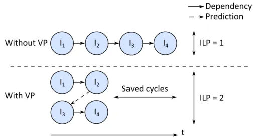
Figure 1: Impact de la prédiction de valeurs (VP) sur la chaîne de dépendances séquentielles exprimée par un programme.
dire ne pouvant pas bénéficier de la présence de plusieurs coeurs. De plus, les programmes parallèles possèdent en général une portion purement séquentielle. Cela implique que même avec une infinité de coeurs pour exécuter la partie par-allèle, la performance sera limitée par la partie séquentielle, c’est la loi d’Amdahl. Par conséquent, même à l’ère des multi-coeurs, il reste nécessaire de continuer à améliorer la performance séquentielle.
Hélas, la façon la plus naturelle d’augmenter la performance séquentielle (aug-menter le nombre d’instructions traitées chaque cycle ainsi que la taille de la fenêtre spéculative d’instructions) est connue pour être très couteuse en tran-sistors et pour augmenter la consommation énergétique ainsi que la puissance dissipée. Il est donc nécessaire de trouver d’autres moyens d’améliorer la perfor-mance sans augmenter la complexité du processeur de façon déraisonnable.
Dans ces travaux, nous revisitions un tel moyen. La prédiction de valeurs (VP) permet d’augmenter le parallélisme d’instructions (le nombre d’instructions pouvant s’exécuter de façon concurrente, ou ILP) disponible en spéculant sur le résultat des instructions. De ce fait, les instructions dépendantes de résultats spéculés peuvent être exécutées plus tôt, augmentant la performance séquentielle. La prédiction de valeurs permet donc une meilleure utilisation des ressources matérielles déjà présentes et ne requiert pas d’augmenter le nombre d’instructions que le processeur peut traiter en parallèle. La Figure 1 illustre comment la prédiction du résultat d’une instruction permet d’extraire plus de parallélisme d’instructions que la sémantique séquentielle du programme n’exprime.
Cependant, la prédiction de valeurs requiert un mécanisme validant les pré-dictions et s’assurant que l’exécution reste correcte même si un résultat est
mal prédit. En général, ce mécanisme est implanté directement dans le cœur d’exécution dans le désordre, qui est déjà très complexe en lui-même. Mettre en œuvre la prédiction de valeurs avec ce mécanisme de validation serait donc contraire à l’objectif de ne pas complexifier le processeur.
De plus, la prédiction de valeurs requiert un accès au fichier de registres, qui est la structure contenant les valeurs des opérandes des instructions à exécuter, ainsi que leurs résultats. En effet, une fois un résultat prédit, il doit être inséré dans le fichier de registres afin de pouvoir être utilisé par les instructions qui en dépendent. De même, afin de valider une prédiction, elle doit être lue depuis le fichier de registres et comparée avec le résultat non spéculatif. Ces accès sont en concurrence avec les accès effectués par le moteur d’exécution dans le désordre, et des ports de lectures/écritures additionnels sont donc requis afin d’éviter les conflits. Cependant, la surface et la consommation du fichier de registres croissent de façon super-linéaire avec le nombre de ports d’accès. Il est donc nécessaire de trouver un moyen de mettre en œuvre la prédiction de valeurs sans augmenter la complexité du fichier de registres.
Enfin, la structure fournissant les prédictions au processeur, le prédicteur, doit être aussi simple que possible, que ce soit dans son fonctionnement ou dans le bud-get de stockage qu’il requiert. Cependant, il doit être capable de fournir plusieurs prédictions par cycle, puisque le processeur peut traiter plusieurs instructions par cycle. Cela sous-entend que comme pour le fichier de registres, plusieurs ports d’accès sont nécessaires afin d’accéder à plusieurs prédictions chaque cycle. L’ajout d’un prédicteur de plusieurs kilo-octets possédant plusieurs ports d’accès aurait un impact non négligeable sur la consommation du processeur, et devrait donc être évité.
Ces trois exigences sont les principales raisons pour lesquelles la prédiction de valeurs n’a jusqu’ici pas été implantée dans un processeur. Dans ces travaux de thèse, nous revisitons la prédiction de valeurs dans le contexte actuel. En par-ticulier, nous proposons des solutions aux trois problèmes mentionnés ci-dessus, permettant à la prédiction de valeurs de ne pas augmenter significativement la complexité du processeur, déjà très élevée. Ainsi, la prédiction de valeurs devient une façon réaliste d’augmenter la performance séquentielle.
Dans un premier temps, nous proposons un nouveau prédicteur tirant parti des avancées récentes dans le domaine de la prédiction de branchement. Ce pré-dicteur est plus performant que les prépré-dicteurs existants se basant sur le contexte pour prédire. De plus, il ne souffre pas de difficultés intrinsèques de mise en œuvre telle que le besoin de gérer des historiques locaux de façon spéculative. Il s’agit là d’un premier pas vers un prédicteur efficace mais néanmoins réalisable. Nous montrons aussi que si la précision du prédicteur est très haute, i.e., les mau-vaises prédictions sont très rares, alors la validation des prédictions peut se faire lorsque les instructions sont retirées du processeurs, dans l’ordre. Il n’est donc
n’ont pas besoin d’être exécutées avant le moment ou elles sont retirées du pro-cesseur, puisque les instructions qui en dépendent peuvent utiliser la prédic-tion comme opérande source. De ce fait, nous proposons un nouveau mod-èle d’exécution, EOLE, dans lequel de nombreuses instructions sont exécutées dans l’ordre, hors du moteur d’exécution dans le désordre. Ainsi, le nombre d’instructions que le moteur d’exécution dans le désordre peut traiter à chaque cycle peut être réduit, et donc le nombre de ports d’accès qu’il requiert sur le fichier de registre. Nous obtenons donc un processeur avec des performances similaires à un processeur utilisant la prédiction de valeurs, mais dont le mo-teur d’exécution dans le désordre est plus simple, et dont le fichier de registres nécessite autant de ports d’accès qu’un processeur sans prédiction de valeurs.
Finalement, nous proposons une infrastructure de prédiction capable de prédire plusieurs instructions à chaque cycle, tout en ne possédant que des structures avec un seul port d’accès. Pour ce faire, nous tirons parti du fait que le processeur exécute les instructions de façon séquentielle, et qu’il est donc possible de grouper les prédictions qui correspondent à des instructions contiguës en mémoire dans une seule entrée du prédicteur. Il devient donc possible de récupérer toutes les prédictions correspondant à un bloc d’instructions en un seul accès au prédicteur. Nous discutons aussi de la gestion spéculative du contexte requis par certains pré-dicteurs pour prédire les résultats, et proposons une solution réaliste tirant aussi parti de l’agencement en bloc des instructions. Nous considérons aussi des façons de réduire le budget de stockage nécessaire au prédicteur et montrons qu’il est possible de n’utiliser que 16-32 kilo-octets, soit un budget similaire à celui du cache de premier niveau ou du prédicteur de branchement.
Au final, nous obtenons une amélioration moyenne des performances de l’ordre de 11.2%, allant jusqu’à 62.2%. Les performances obtenues ne sont jamais in-férieures à celles du processeur de référence (i.e., sans prédiction de valeurs) sur les programmes considérés. Nous obtenons ces chiffres avec un processeur dont le moteur d’exécution dans le désordre est significativement moins complexe que dans le processeur de référence, tandis que le fichier de registres est équivalent au fichier de registres du processeur de référence. Le principal coût vient donc du prédicteur de valeur, cependant ce coût reste raisonnable dans la mesure où il est possible de mettre en œuvre des tables ne possédant qu’un seul port d’accès.
Ces trois contributions forment donc une mise en œuvre possible de la prédic-tion de valeurs au sein d’un processeur généraliste haute performance moderne, et proposent donc une alternative sérieuse à l’augmentation de la taille de la fenêtre spéculative d’instructions du processeur afin d’augmenter la performance séquentielle.
Processors – in their broader sense, i.e., general purpose or not – are effectively the cornerstone of modern computer science. To convince ourselves, let us try to imagine for a minute what computer science would consist of without such chips. Most likely, it would be relegated to a field of mathematics as there would not be enough processing power for graphics processing, bioinformatics (including DNA sequencing and protein folding) and machine learning to simply exist. Languages and compilers would also be of much less interest in the absence of machines to run the compiled code on. Evidently, processor usage is not limited to computer science: Processors are everywhere, from phones to cars, to houses, and many more.
Yet, processors are horrendously complex to design, validate, and manufac-ture. This complexity is often not well understood by their users. To give an idea of the implications of processor design, let us consider the atomic unit of a modern processor: the transistor. Most current generation general purpose microprocessor feature hundreds of millions to billions of transistors. By con-necting those transistors in a certain fashion, binary functions such as OR and AND can be implemented. Then, by combining these elementary functions, we obtain a device able to carry out higher-level operations such as additions and multiplications. Although all the connections between transistors are not explic-itly designed by hand, many high-performance processors feature custom logic where circuit designers act at the transistor level. Consequently, it follows that designing and validating a processor is extremely time and resource consuming.
Moreover, even if modern general purpose processors possess the ability to perform billions of arithmetic operations per second, it appears that to keep a steady pace in both computer science research and quality of life improvement, processors should keep getting faster and more energy efficient. Those represent the two main challenges of processor architecture.
To achieve these goals, the architect acts at a level higher than the transistor but not much higher than the logic gate (e.g., OR, AND, etc.). In particular, he or she can alter the way the different components of the processor are connected, the way they operate, and simply add or remove components. This is in contrast with the circuit designer that would improve performance by rearranging
or she should keep the laws of physics in mind when drawing his or her plans. In general, processor architecture is about tradeoffs. For instance, tradeoffs between simplicity ("My processor can just do additions in hardware, but it was easy to build") and performance ("The issue is that divisions are very slow be-cause I have to emulate them using additions"), or tradeoffs between raw compute power ("My processor can do 4 additions at the same time") and power efficiency ("It dissipates more power than a vacuum cleaner to do it"). Therefore, in a nutshell, architecture consists in designing a computer processor from a reason-ably high level, by taking into account those tradeoffs and experimenting with new organizations. In particular, processor architecture has lived through several paradigm shifts in just a few decades, going from 1-cycle architectures to modern deeply pipelined superscalar processors, from single core to multi-core, from very high frequency to very high power and energy efficiency. Nonetheless, the goals remain similar: increase the amount of work that can be done in a given amount of time, while minimizing the energy spent doing this work.
Overall, there are two main directions to improve processor performance. The first one leverages the fact that processors are clocked objects, meaning that when the associated clock ticks, then some computation step has finished. For instance, a processor may execute one instruction per clock tick. Therefore, if the clock speed of the processor is increased, then more work can be done in a given unit of time, as there are now more clock ticks in said unit of time. However, as the clock frequency is increased, the power consumption of the processor grows super-linearly,2 and quickly becomes too high to handle. Moreover, transistors
possess an intrinsic maximum switching frequency and a signal can only travel so far in a wire in a given clock period. Exceeding these two limits would lead to unpredictable results. For these reasons, clock frequency has generally remained comprised between 2GHz and 5GHz in the last decade, and this should remain the case for the same reasons.
Second, thanks to improvements in transistor implantation processes, more and more transistors can be crammed in a given surface of silicon. This
phe-2Since the supply voltage must generally grow as the frequency is increased, power
con-sumption increases super-linearly with frequency. If the supply voltage can be kept constant somehow, then the increase should be linear.
nomenon is embodied by Moore’s Law, that states that the number of transistors than can be implanted on a chip doubles every 24 months [Moo98]. Although it is an empirical law, it has proven exactly right between 1971 and 2001. However, increase has slowed down during the past decade. Nonetheless, consider that the Intel 8086 released in 1978 had between 20,000 and 30,000 transistors while some modern Intel processors have more than 2 billions, that is 100,000 times more.3
However, if a tremendous number of transistors are available to the architect, it is becoming extremely hard to translate these additional transistors into additional performance.
In the past, substantial performance improvements due to an increased num-ber of transistors came from the improvement of uni-processors through pipelin-ing, superscalar execution and out-of-order execution. All those features target sequential performance, i.e., the performance of a single processor. However, it has become very hard to keep on targeting sequential performance with the additional transistors we get, because of diminishing returns. Therefore, as no new paradigm was found to replace the current one (superscalar out-of-order execution), the trend regarding high performance processors has shifted from uni-processor chips to multi-processor chips. This allows to obtain a performance increase on par with the additional transistors provided by transistor technology, keeping Moore’s Law alive in the process.
More specifically, an intuitive way to increase the performance of a program is to cut it down into several smaller programs that can be executed concur-rently. Given the availability of many transistors, multiple processors can be implemented on a single chip, with each processor able to execute one piece of the initial program. As a result, the execution time of the initial program is decreased. This not-so-new paradigm targets parallel performance (i.e., through-put: how much work is done in a given unit of time), as opposed to sequential performance (i.e., latency or response time: how fast can a task finish).
However, this approach has two limits. First, some programs may not be parallel at all due to the nature of the algorithm they are implementing. That is, it will not be possible to break them down into smaller programs executed concurrently, and they will therefore not benefit from the additional processors of the chip. Second, Amdahl’s Law [Amd67] limits the performance gain that can be obtained by parallelizing a program. Specifically, this law represents a program as a sequential part and a parallel part, with the sum of those parts adding up to 1. Among those two parts, only the parallel one can be sped up by using several processors. For instance, for a program whose sequential part is equivalent to the parallel part, execution time can be reduced by a factor of 2 at most, that is if there is an infinity of processors to execute the parallel part. Therefore, even
Processors (CMP, several processors on a single chip a.k.a. multi-cores). They can therefore be added on-top of existing hardware. Furthermore, if this thesis fo-cuses on the design step of processor conception, technology constraints are kept in mind. In other words, specific care is taken to allow the proposed mechanisms to be realistically implementable using current technology.
Contributions
We revisit a mechanism aiming to increase sequential performance: Value Pre-diction (VP). The key idea behind VP is to predict instruction results in order to break dependency chains and execute instructions earlier than previously pos-sible. In particular, for out-of-order processors, this leads to a better utilization of the execution engine: Instead of being able to uncover more Instruction Level Parallelism (ILP) from the program by being able to look further ahead (e.g., by having a larger instruction window), the processor creates more ILP by breaking some true dependencies in the existing instruction window.
VP relies on the fact that there exist common instructions (e.g., load, read data from memory) that can take up to a few hundreds of processor cycles to execute. During this time, no instruction requiring the data retrieved by the load instruction can be executed, most likely stalling the whole processor. Fortunately, many of these instructions often produce the same result, or results that follow a pattern, which could therefore be predicted. Consequently, by predicting the result of a load instruction, dependents can execute while the memory hierarchy is processing the load. If the prediction is correct, execution time decreases, otherwise, dependent instructions must be re-executed with the correct input to enforce correctness.
Our first contribution [PS14b] makes the case that contrarily to previous im-plementations described in the 90’s, it is possible to add Value Prediction on top of a modern general purpose processor without adding tremendous complexity in its pipeline. In particular, it is possible for VP to intervene only in the front-end of the pipeline, at Fetch (to predict), and in the last stage of the back-end, Com-mit (to validate predictions and recover if necessary). Validation at ComCom-mit is
rendered possible because squashing the whole pipeline can be used to recover from a misprediction, as long as value mispredictions are rare. This is in con-trast with previous schemes where instructions were replayed directly inside the out-of-order window. In this fashion, all the – horrendously complex – logic re-sponsible for out-of-order execution need not be modified to support VP. This is a substantial improvement over previously proposed implementations of VP that coupled VP with the out-of-order execution engine tightly. In addition, we intro-duce a new hybrid value predictor, D-VTAGE, inspired from recent advances in the field of branch prediction. This predictor has several advantages over exist-ing value predictors, both from a performance standpoint and from a complexity standpoint.
Our second contribution [PS14a, PS15b] focuses on reducing the additional Physical Register File (PRF) ports required by Value Prediction. Interestingly, we achieve this reduction because VP actually enables a reduction in the com-plexity of the out-of-order execution engine. Indeed, an instruction whose result is predicted does not need to be executed as soon as possible, since its dependents can use the prediction to execute. Therefore, we introduce some logic in charge of executing predicted instructions as late as possible, just before they are removed from the pipeline. These instructions never enter the out-of-order window. We also notice that thanks to VP, many instructions are ready to be executed very early in the pipeline. Consequently, we also introduce some logic in charge of exe-cuting such instructions in the front-end of the pipeline. As a result, instructions that are executed early are not even dispatched to the out-of-order window. With this {Early | Out-of-Order | Late} (EOLE) architecture, a substantial portion of the dynamic instructions is not executed inside the out-of-order execution engine, and said engine can be simplified by reducing its issue-width, for instance. This mechanically reduces the number of ports on the register file, and is a strong ar-gument in favor of Value Prediction since the complexity and power consumption of the out-of-order execution engine are already substantial.
Our third and last contribution [PS15a] relates to the design of a realistic pre-dictor infrastructure allowing the prediction of several instructions per cycle with single-ported structures. Indeed, modern processors are able to retrieve several instructions per cycle from memory, and the predictor should be able to provide a prediction for each of them. Unfortunately, accessing several predictor entries in a single cycle usually requires several access ports, which should be avoided when considering such a big structure (16-32KB). To that extent, we propose a block-based prediction infrastructure that provides predictions for the whole in-struction fetch block with a single read in the predictor. We achieve superscalar prediction even when a variable-length instruction set such as x86 is used. We show that combined to a reasonably sized D-VTAGE predictor, performance im-provements are close to those obtained by using an ideal infrastructure combined
interactions between VP and the engine to the register file only. Moreover, we provide two structures that execute instructions either early or late in the pipeline, offloading the execution of many instructions from the out-of-order engine. As a result, it can be made less aggressive, and VP viewed as a means to reduce complexity rather than increase it. Finally, by devising a better predictor inspired from recent branch predictors and providing a mechanism to make it single-ported, we are able to outperform previous schemes and address complexity in the predictor infrastructure.
Organization
This document is divided in five chapters and architected around three published contributions: two in the International Symposium on High Performance Com-puter Architecture (HPCA 2014/15) [PS14b, PS15a] and one in the International Symposium on Computer Architecture (ISCA 2014) [PS14a].
Chapter 1 provides a description of the inner workings of modern general purpose processors. We begin with the simple pipelined architecture and then improve on it by following the different processor design paradigms in a chrono-logical fashion. This will allow the reader to grasp why sequential performance bottlenecks remain in deeply pipelined superscalar processors and understand how Value Prediction can help mitigate at least one of such bottlenecks.
Chapter 2 introduces Value Prediction in more details and presents previous work. Existing hardware prediction algorithms are detailed and their advantages and shortcomings discussed. In particular, we present computational predictors that compute a prediction from a previous result and context-based predictor that provide a prediction when some current information history matches a previously seen pattern [SS97a]. Then, we focus on how VP – and especially prediction val-idation – has usually been integrated with the pipeline. Specifically, we illustrate how existing implementations fall short of mitigating the complexity introduced by VP in the out-of-order execution engine.
Chapter 3 focuses on our first [PS14b] and part of our third [PS15a] contri-butions. We describe a new predictor, VTAGE, that does not suffer from the
shortcomings of existing context-based predictors. We then improve on it by hy-bridizing it with a computational predictor in an efficient manner and present Differential VTAGE (D-VTAGE). In parallel, we show that Value Prediction can be plugged into an existing pipeline without increasing complexity in parts of the pipeline that are already tremendously complex. We do so by delaying prediction validation and prediction recovery until in-order retirement.
Chapter 4 goes further by showing that Value Prediction can be leveraged to actually reduce complexity in the out-of-order window of a modern processor. By enabling a reduction in the out-of-order issue-width through executing instruction early or late in the pipeline, the EOLE architecture [PS14a] outperforms a wider processor while having 33% less out-of-order issue capacity and the same number of register file ports.
Finally, Chapter 5 comes back to the predictor infrastructure and addresses the need to provide several predictions per cycle in superscalar processors. We detail our block-based scheme enabling superscalar value prediction. We also propose an implementation of the speculative window tracking inflight predictions that is needed to compute predictions in many predictors [PS15a]. Lastly, we study the behavior of the D-VTAGE predictor presented in Chapter 2 when its storage budget is reduced to a more realistic 16-32KB.
The Architecture of a Modern
General Purpose Processor
General purpose processors are programmable devices, hence, they present an interface to the programmer known as the Instruction Set Architecture or ISA. Among the few widely used ISA, the x86 instruction set of Intel stands out from the rest as it remained retro-compatible across processor generations. That is, a processor bought in 2015 will be able to execute a program written for the 8086 (1978). Fortunately, this modern processor will be much faster than a 8086. As a result, it is important to note that the interface exposed to the software is not necessarily representative of the underlying organization of the processor and therefore its computation capabilities. It is required to distinguish between the architecture or ISA (e.g., x86, ARMv7, ARMv8, Alpha) from the micro-architecture implementing the micro-architecture on actual silicon (e.g. Intel Haswell or AMD Bulldozer for x86, ARM Cortex A9 or Qualcomm Krait for ARMv7). In this thesis, we focus on the micro-architecture of a processor and aim to remain agnostic of the actual ISA.
1.1
Instruction Set – Software Interface
Each ISA defines a set of instructions and a set of registers. Registers can be seen as scratchpads from which instructions read their operands and to which instructions write their results. They also define an address space used to access global memory, which can be seen as a backing store for registers. These three components are visible to the software, and they form the interface with which the processor can be programmed to execute a specific task.
The distinction is often made between Reduced Instruction Set Computer ISAs (RISC) and Complex Instruction Set Computer ISAs (CISC). The former indi-cates that instructions visible to the programmer are usually limited to simple
bit) while the most widely used CISC ISA is x86 in its 64-bit version (x86_64). 32- and 64-bit refer to the width of the – virtual – addresses used to access global memory. That is, ARMv7 can only address 232 memory locations (4 GB), while ARMv8 and x86_64 can address 264 memory locations (amounting to 16 EB).
1.1.1
Instruction Format
The instructions of a program are stored in global memory using a binary repre-sentation. Each particular ISA defines how instructions are encoded. Nonetheless, there exists two main paradigms for instruction encoding.
First, a fixed-length can be used, for instance 4 bytes (32 bits) in ARMv7. These 4 bytes contain – among other information – an opcode (the nature of the operation to carry out), two source registers and one destination register. In that case, decoding the binary representation of the instruction to generate the control signals for the rest of the processor is generally straightforward. Indeed, each field is always stored at the same offset in the 4-byte word. Unfortunately, memory capacity is wasted for instructions that do not need two sources (e.g., incrementing a single register) or that do not produce any output (e.g., branches). Conversely, a variable-length can be used to encode different instructions. For instance, in x86, instructions can occupy 1 to 15 bytes (120 bits!) in memory. As a result, instruction decoding is much more complex as the location of a field in the instruction word (e.g., the first source register) depends on the value of previous fields. Moreover, since an instruction has variable-length, it is not straightforward to identify where the next instruction is. Nonetheless, variable-length representation is generally more storage-efficient.
1.1.2
Architectural State
Each ISA defines an architectural state. It is the state of the processor that is visible by the programmer. It consists of all registers1 defined by the ISA as well
as the state of global memory, and it is agnostic of which program is currently
1Including the Program Counter (PC) pointing to the memory location containing the
being executed on the processor. The instructions defined by the ISA operate on this architectural state. For instance, an addition will take the architectural state as its input (or rather, a subset of the architectural state) and output a value that will be put in a register, hence modify the architectural state. From the software point of view, this modification is atomic: there is no architectural state between the state before the addition and the state after the addition.
Consequently, a program is a sequence of instructions (as defined by the ISA) that keeps on modifying the architectural state to compute a result. It follows that programs running on the processor have sequential semantics. That is, from the point of view of the software, the architectural state is modified atomically by instructions following the order in which they appear in the program. In practice, the micro-architecture may work on its own internal version of the architectural state as it pleases, as long as updates to the software-visible architectural state respect atomicity and the sequential semantics of the program. In the remainder of this document, we differentiate between the software-visible state and any speculative (i.e., not software-visible yet) state living inside the processor.
1.2
Simple Pipelining
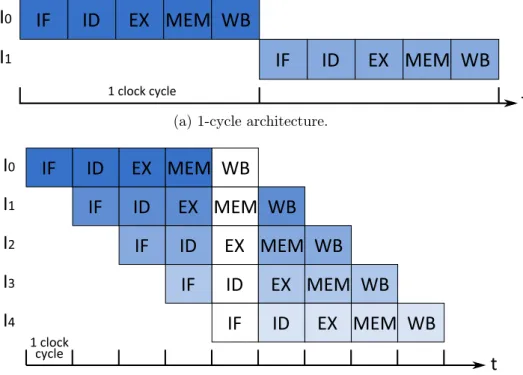
Processors are clocked devices, meaning that they are driven by a clock that ticks a certain number of times per second. Each tick triggers the execution of some work in the processor. Arguably, the most intuitive micro-architecture is therefore the 1-cycle micro-architecture where the operation triggered by the clock tick is the entire execution of an instruction. To guarantee that this is possible, the clock has to tick slow enough to allow the slowest (the one requiring the most processing) instruction to execute in a single clock cycle.
Regardless, the execution of an instruction involves several very different steps requiring very different hardware structures. In a 1-cycle micro-architecture, a single instruction flows through all these hardware structures during the clock cycle. Assuming there are five steps to carry out to actually execute the instruc-tion and make its effects visible to the software, this – roughly – means that each of the five distinct hardware structures is idle during four-fifth of the clock cycle. As a result, this micro-architecture is highly inefficient.
Pipelined micro-architectures were introduced to remedy this issue. The high-level idea is that since an instruction flows sequentially through several stages to be processed, there is potential to process instruction I0 in stage S1 while
instruction I1 is concurrently processed in stage S0. Therefore, resources are
much better utilized thanks to this pipeline parallelism. Moreover, instead of considering the slowest instruction when choosing cycle time, only the delay of the slowest pipeline stage has to be considered. Therefore, cycle time can be
(b) Simple 5-stages pipeline. As soon as the pipeline is filled (shown in white), all stages are busy processing different instructions every cycle.
Figure 1.1: Pipelined execution: x-axis shows time in cycles while y-axis shows sequential instructions.
decreased.
Both 1-cycle architecture and simple 5-stages pipeline are depicted in Figure 1.1. In this example, a single stage takes a single cycle, meaning that around five cycles are required to process a single instruction in the pipeline shown in (b). Nonetheless, as long as the pipeline is full, one instruction finishes execution each cycle, hence the throughput of one instruction per cycle is preserved. Moreover, since much less work has to be done in a single cycle, cycle time can be decreased as pipeline depth increases. As a result, performance increases, as illustrated in Figure 1.1 where the pipeline in (b) can execute five instructions in less time than the 1-cycle architecture in (a) can execute two, assuming the cycle time of the former is one fifth of the cycle time of the latter.
One should note, however, that as the pipeline depth increases, we start to observe diminishing returns. The reasons are twofold. First, very high frequency (above 4GHz) should be avoided to limit power consumption, hence deepening the pipeline to increase frequency quickly becomes impractical. Second, struc-tural hazards inherent to the pipeline structure and the sequential processing of instructions makes it inefficient to go past 15/20 pipeline cycles. Those hazards will be described in the next Section.
1.2.1
Different Stages for Different Tasks
In the following paragraphs, we describe how the execution of an instruction can be broken down into several steps. Note that it is possible to break down these steps even further, or to add more steps depending on how the micro-architecture actually processes instructions. In particular, we will see in 1.3.3 that additional steps are required for out-of-sequence execution.
1.2.1.1 Instruction Fetch – IF
As previously mentioned, the instructions of the program to execute reside in global memory. Therefore, the current instruction to execute has to be brought into the processor to be processed. This requires accessing the memory hierarchy with the address contained in the Program Counter (PC) and updating the PC for the next cycle.
1.2.1.2 Instruction Decode – ID
The instruction retrieved by the Fetch stage is encoded in a binary format to occupy less space in memory. This binary word has to be expanded – decoded – into the control word that will drive the rest of the pipeline (e.g., register indexes to access the register file, control word of the functional unit, control word of the datapath multiplexers, etc.). In the pipeline we consider, Decode includes reading sources from the Physical Register File (PRF), although a later stage could be dedicated to it, or it could be done at Execute.
For now, we only consider the case of a RISC pipeline, but in the case of CISC, the semantics of many instructions are too complex to be handled by the stages following Decode as is. Therefore, the Decode stage is in charge of cracking such instructions into several micro-operations (µ-ops) that are more suited to the hardware. For instance, a load instruction may be cracked into a µ-op that computes the address from which to load the data from, and a µ-op that actually accesses the memory hierarchy.
1.2.1.3 Execute – EX
This stage actually computes the result of the instruction. In the case of load instructions, address calculation is done in this stage, while the access to the memory hierarchy will be done in the next stage, Memory.
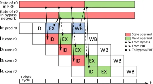
To allow the execution of two dependent instructions back-to-back, the result of the first instruction is made available to the second instruction on the bypass network. In this particular processor, the bypass network spans from Execute to Writeback, at which point results are written to the PRF. For instance, let us
Figure 1.2: Origin of the operands of four sequential instructions dependent on a single instruction. Some stage labels are omitted for clarity.
consider Figure 1.2 where I1, I2, I3and I4 all require the result of I0. I1 will catch
its source r0 on the bypass network since I0 is in the Memory stage when I1 is in
Execute. I2 will also catch r0 on the network because I0 is writing back its result
to the PRF when I2 is in Execute. Interestingly, I3 will also catch its source on
the network since when I3 read its source registers in the Decode stage, I0 was
writing its result to the PRF, therefore, I3 read the old value of the register. As
a result, only I4 will read r0 from the PRF.
Without the bypass network, a dependent instruction would have to wait until the producer of its source left Writeback2 before entering the Decode stage and
reading it in the PRF. In our pipeline model, this would amount to a minimum delay of 3 cycles between any two dependent instructions. Therefore, the bypass network is a key component of pipelined processor performance.
1.2.1.4 Memory – MEM
In this stage, all instructions requiring access to the memory hierarchy proceed with said access. In modern processors, the memory hierarchy consists of sev-eral levels of cache memory intercalated between the pipeline and main memory. Cache memories contain a subset of main memory, that is, a datum that is in the cache also resides in main memory3.
We would like to stress that contrarily to scratchpads, caches are not managed by the software and are therefore transparent to the programmer. Any memory
2Results are written to the PRF in Writeback.
3Note that a more recent version of the datum may reside in the cache and be waiting to be
Figure 1.3: 3-level memory hierarchy. As the color goes from strong green to red, access latency increases. WB stands for writeback.
the L2 is written back to the next lower level of the hierarchy (potentially main memory), and so on.
An organization with two levels4 of cache is shown in Figure 1.3. The first
level of cache is the smallest but also the fastest, and as we go down the hierarchy, size increases but so does latency. In particular, an access to the first cache level only requires a few processor cycles while going to main memory can takes up to several hundreds of processor cycles and stall the processor in the process. As a result, thanks to temporal5 and spatial6 locality, caches allow memory accesses to be very fast on average, while still providing the full storage capacity of main memory to the processor.
1.2.1.5 Writeback – WB
This stage is responsible for committing the computed result (or loaded value) to the PRF. As previously mentioned, results in flight between Execute and Write-back are made available to younger instructions on the bypass network. In this simple pipeline, once an instruction leaves the Writeback stage, its execution has completed and from the point of view of the software, the effect of the instruction on the architectural state is now visible.
1.2.2
Limitations
Control Hazards In general, branches are resolved at Execute. Therefore, an issue related to control flow dependencies begins to emerge when pipelining is used. Indeed, when a conditional branch leaves the Fetch stage, the processor does not know which instruction to fetch next because it does not know what direction the branch will take. As a result, the processor should wait for the branch to be resolved until it can continue fetching instructions. Therefore, bubbles (no operation) must be inserted in the pipeline until the branch outcome is known.
4Modern Chip Multi-Processors (CMP, a.k.a. multi-cores) usually possess a L3 cache shared
between all cores. Its size ranges from a few MB to a few tens of MB.
5Recently used data is likely to be re-used soon.
Figure 1.4: Control hazard in the pipeline: new instructions cannot enter the pipeline before the branch outcome is known.
In this example, this would mean stalling the pipeline for two cycles on each branch instruction, as illustrated in Figure 1.4. In general, a given pipeline would be stalled for Fetch-to-Execute cycles, which may amount to a few tens of cycles in some pipelines (e.g., Intel Pentium 4 has a 20/30-stages pipeline depending on the generation). Therefore, if deepening the pipeline allows to increase processor speed by decreasing the cycle time, the impact of control dependencies quickly becomes prevalent and should be addressed [SC02].
Data Hazards Although the bypass network increases efficiency by forwarding values to instructions as soon as they are produced, the baseline pipeline also suffers from data hazards. Data hazards are embodied by three types of register dependencies.
On the one hand, true data dependencies, also called Read-After-Write (RAW ) dependencies cannot generally be circumvented as they are intrinsic to the algo-rithm that the program implements. For instance, in the expression (1 + 2 ∗ 3), the result of 2 ∗ 3 is always required before the addition can be done. Unfortu-nately, in the case of long latency operations such as a load missing in all cache levels, a RAW dependency between the load and its dependents entails that said dependents will be stalled for potentially hundreds of cycles.
On the other hand, there are two kind of false data dependencies. They both exist because of the limited number of architectural registers defined by the ISA (only 16 in x86_64). That is, if there were an infinite number of registers, they would not exist. First, Write-after-Write (WAW ) hazards take place when two instructions plan to write to the same architectural register. In that case, writes must happen in program order. This is already enforced by the in-order
execution). However, in this case, WAW and WAR hazards become a substantial hindrance to the efficient processing of instructions. Indeed, they forbid two inde-pendent instructions to be executed out-of-order simply because both instructions write to the same architectural register (case of WAW dependencies). The reason behind this name collision is that ISAs only define a few number of architectural registers. As a result, the compiler often does not have enough architectural registers (i.e., names) to attribute a different one to each instruction destination.
1.3
Advanced Pipelining
1.3.1
Branch Prediction
As mentioned in the previous section, the pipeline must introduce bubbles instead of fetching instructions when an unresolved branch is in flight. This is because neither the direction of the branch nor the address from which to fetch next should the branch be taken are known. To address this issue, Branch Prediction was introduced [Smi81]. The key idea is that when a branch is fetched, a predictor is accessed, and a predicted direction and branch target are retrieved.
Naturally, because of the speculative nature of branch prediction, it will be necessary to throw some instructions away when the prediction is found out to be wrong. In our 5-cycle pipeline where branches are resolved at Execute, this would translate in two instructions being thrown away on a branch misprediction. Fortunately, since execution is in-order, no rollback has to take place, i.e., the instructions on the wrong path did not incorrectly modify the architectural state. Moreover, in this particular pipeline, the cost of never predicting is similar to the cost of always mispredicting. Therefore, it follows that adding branch prediction would have a great impact on performance even if one branch out of two was mispredicted. This is actually true in general although mispredicting has a mod-erately higher cost than not predicting. Nonetheless, branch predictors are gener-ally able to attain an accuracy in the range of 0.9 to 0.99 [SM06, Sez11b, cbp14], which makes branch prediction a key component of processor performance.
Although part of this thesis work makes use of recent advances in branch prediction, we do not detail the inner workings of existing branch predictors in
this Section. We will only describe the TAGE [SM06] branch predictor in Chapter 3 as it is required for our VTAGE value predictor. Regardless, the key idea is that given the address of a given branch instruction and some additional processor state (e.g., outcome of recent branches), the predictor is able to predict the branch direction. The target of the branch is predicted by a different – though equivalent in the input it takes – structure and can in some cases be computed at Decode instead of Execute.
1.3.2
Superscalar Execution
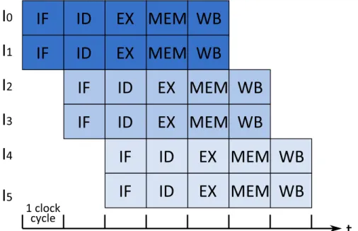
In a sequence of instructions, it is often the case that two or more neighbor-ing instructions are independent. As a result, one can increase performance by processing those instructions in parallel. For instance, pipeline resources can be duplicated, allowing several instructions to flow in the pipeline in parallel, al-though still following program order. That is, by being able to fetch, decode, execute and writeback several instructions per cycle, throughput can be greatly increased, as long as instructions are independent. If not, only a single instruction can proceed while subsequent ones are stalled.
For instance, in Figure 1.5, six instructions can be executed by pairs in a pipeline having a superscalar degree of 2 (i.e., able to process two instructions concurrently). One should note that only 7 cycles are required to execute those instructions while the scalar pipeline of Figure 1.1 (b) would have required 10 cycles.
Unfortunately, superscalar execution has great hardware cost. Indeed, if creasing the width of the Fetch stage is fairly straightforward up to a few in-structions (get more bytes from the instruction cache), the Decode stage is now in charge of decoding several instructions and resolving any dependencies be-tween them to determine if they can proceed further together or if one must stall. Moreover, if functional units can simply be duplicated, the complexity of the bypass network in charge of providing operands on-the-fly grows quadratically with the superscalar degree. Similarly, the PRF must now handle 4 reads and 2 writes per cycle instead of 2 reads and 1 write in a scalar pipeline, assuming two sources and one destination per instruction. Therefore, ports must be added on the PRF, leading to a much higher area and power consumption since both grow super-linearly with the port count [ZK98]. The same stands for the L1 cache if one wants to enable several load instructions to proceed each cycle.
In addition, this implementation of a superscalar pipeline is very limited in how much it can exploit the independence between instructions. Indeed, it is not able to process concurrently two independent instructions that are a few in-structions apart in the program. It can only process concurrently two neighboring instructions, because it executes in-order. This means that a long latency
instruc-Figure 1.5: Degree 2 superscalar pipeline: two instructions can be processed by each stage each cycle as long as they are independent.
tion will still stall the pipeline even if an instruction further down the program is ready to execute. Even worse, due to the unpredictable behavior of program execution (e.g., cache misses, branch mispredictions) and the limited number of architectural registers, the compiler is not always able to reorder instructions in a way that can leverage this independence. As a result, increasing the superscalar degree while maintaining in-order execution is not cost-efficient. To circumvent this limitation, out-of-order execution [Tom67] was proposed and is widely used in modern processors.
1.3.3
Out-of-Order Execution
1.3.3.1 Key Idea
Although modern ISAs have sequential semantics, many instructions of a given program are independent on one another, meaning that they could be executed in any order. This phenomenon is referred to as Instruction Level Parallelism or ILP.
As a result, most current generation processors implement a feature known as out-of-order execution (OoO) that allows them to reorder instructions in hard-ware. To preserve the sequential semantics of the programs, instructions are still fetched in program order, and the modifications they apply on the architectural state are also made visible to the software in program order. It is only the
exe-cution that happens out-of-order, driven by true data dependencies (RAW) and resource availability.
To ensure that out-of-order provides both high performance and sequential semantics, numerous modifications must be made to our existing 5-stage pipeline.
1.3.3.2 Register Renaming
We previously presented the three types of data dependencies: RAW, WAW and WAR. We mentioned that WAW and WAR are false dependencies, and that in an in-order processor, they are a non-issue since in-order execution prohibits them by construction. However, in the context of out-of-order execution, these two types of data dependencies become a major hurdle to performance.
Indeed, consider two independent instructions I0 and I7 that belong to
differ-ent dependency chains, but both write to register r0 simply because the compiler was not able to provide them with distinct architectural registers. As a result, the hardware should ensure that any instruction dependent on I0 can get the
correct value for that register before I7 overwrites it. In general, this means that
a substantial portion of the existing ILP will be inaccessible because the desti-nation names of independent instructions collide. However, if the compiler had had more architectural registers to allocate, the previous dependency would have disappeared. Unfortunately, this would entail modifying the ISA.
A solution to solve this issue is to provide more registers in hardware but keep the number of registers visible to the compiler the same. This way, the ISA does not change. Then, the hardware can dynamically rename architectural registers to physical registers residing in the PRF. In the previous example, I0 could see
its architectural destination register, ar0 (arch. reg 0), renamed to pr0 (physical register 0). Conversely, I7 could see its architectural destination register, also ar0,
renamed to pr1. As a result, both instructions could be executed in any order without overwriting each other’s destination register. The reasoning is exactly the same for WAR dependencies.
To track register mappings, a possibility is to use a Rename Map and a Free List. The Rename Map gives the current mapping of a given architectural register to a physical register. The Free List keeps track of physical registers that are not mapped to any architectural register, and is therefore in charge of providing physical registers to new instructions entering the pipeline. These two steps, source renaming and destination renaming are depicted in Figure 1.6.
Note however that the mappings in the Rename Map are speculative by nature since renamed instructions may not actually be retained if, for instance, an older branch has been mispredicted. Therefore, a logical view of the renaming process includes a Commit Rename Map that contains the non-speculative mappings, i.e., the current software-visible architectural state of the processor. When an
Figure 1.6: Register renaming. Left: Both instruction sources are renamed by looking up the Rename Table. Right: The instruction destination is renamed by mapping a free physical register to it.
Figure 1.7: Introduction of register renaming in the pipeline. The new stage, Rename, is shown in dark blue.
instruction finishes its execution and is removed from the pipeline, the mapping of its architectural destination register is now logically part of the Commit Rename Map.
A physical register is put back in the Free List once a younger instruction mapped to the same architectural register (i.e., that has a more recent mapping) leaves the pipeline.
Rename requires its own pipeline stage(s), and is usually intercalated between Decode and the rest of the pipeline, as shown in Figure 1.7. Thus, it is not possible to read the sources of an instruction in the Decode stage anymore. Moreover, to enforce the sequential semantics of the program, Rename must happen in program order, as Fetch and Decode. Lastly, note that as the superscalar degree increases, the hardware required to rename registers becomes slower as well as more complex [PJS97], since among a group of instruction being renamed in the
same cycle, some may depend on others. In that case, the younger instructions require the destination mappings of the older instructions to rename their sources, but those mappings are being generated. An increased superscalar degree also puts pressure on the Rename Table since it must support that many more reads and writes each cycle.
1.3.3.3 In-order Dispatch and Commit
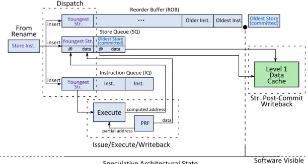
To enable out-of-order execution, instruction scheduling must be decoupled from in-order instruction fetching and in-order instruction retirement. This decoupling is achieved with two structures: The Reorder Buffer (ROB) and the Instruction Queue (IQ) or Scheduler.
The first structure contains all the instructions that have been fetched so far but have not completed their execution. The ROB is a First In First Out (FIFO) queue in which instructions are added at the tail and removed at the head. Therefore, the visible architectural state of the processor (memory state and Commit Rename Map) corresponds to the last instruction that was removed from the ROB.7Moreover, when a branch misprediction is detected when a branch
flows through Execute, the ROB allows to remove all instructions on the wrong path (i.e., younger than the branch) while keeping older instructions. As a result, the ROB is really a speculative frame representing the near future state of the program. In other words, it contains instructions whose side-effects will soon be visible by the software, as long as everything goes well (i.e., control flow is correct, no interruption arrives, no exception is raised).
Conversely, the IQ is a fully associative buffer from which instructions are selected for execution based on operand readiness each cycle. As a result, the IQ is the only structure where instructions can appear and be processed out-of-order. As instructions are executed, they advance towards the head of the ROB where their modifications to the architectural state will be committed. In particular, once an instruction reaches the head of the ROB, the last stage of the pipeline, the Commit stage is in charge of checking if the instruction can be removed, as illustrated in the right part of Figure 1.8. An instruction cannot commit if, for instance, it has been not executed.
Both structures are populated in-order after instruction registers have been renamed, as shown in the left part of Figure 1.8. We refer to this step as instruc-tion dispatch, and to the corresponding pipeline stage as Dispatch. Similarly, instructions are removed from the ROB in program order by the Commit stage, to enforce sequential semantics. Commit is also responsible for handling any ex-ception. These two additional stages are depicted in Figure 1.9. The four first stages in the Figure form what is commonly referred to as the pipeline frontend.
Figure 1.8: Operation of the Dispatch and Commit stages. Left: Instructions from Rename are inserted in the ROB and IQ by Dispatch. Right: In the mean-time, the Commit logic examines the oldest instruction (head of ROB) and re-moves it if it has finished executing.
Figure 1.9: Introduction of instruction dispatch and retirement in the pipeline. The new stages, Dispatch and Commit, are shown in dark blue.
1.3.3.4 Out-of-Order Issue, Execute and Writeback
Operation The IQ is responsible for instruction scheduling or issuing. Each cycle, logic scans the IQ for n instructions8 whose sources are ready i.e., in the
PRF or the bypass network. These selected instructions are then issued to the functional units for execution, with no concern for their ordering. To carry out scheduling, a pipeline stage, Issue, is required.
Before being executed on the functional units (FUs), issued instructions will read their sources from either the PRF or the bypass network in a dedicated stage we refer to as Register/Bypass Read (RBR). In the two subsequent stages, Execute and Writeback, selected instructions will respectively execute and write their result to the PRF. Instruction processing by this four stages is depicted in Figure 1.10.
Note that if two dependent instructions I0 and I1 execute back-to-back, then
the destination of I0 (respectively source of I1) is not available on the multiplexer
of the RBR stage when I1 is in RBR. Consequently, in this case, the bypass
net-work is able to forward the result of I0 from the output of the FU used by I0
during the previous cycle to the input of the FU used by I1 when I1 enters
Exe-cute. The bypass network is therefore multi-level. Also consider that a hardware implementation may not implement several levels of multiplexers as in Figure 1.10, but a single one where results are buffered for a few cycles and tagged with the physical register they correspond to. In that case, an instruction may check the network with its source operands identifiers to get their data from the network.
These four stages form the out-of-order engine of the processor, and are de-coupled from the in-order frontend and in-order commit by the IQ itself. The resulting 9-stage pipeline is shown in Figure 1.11.
Complexity It should be mentioned that the logic used in the out-of-order engine is complex and power hungry. For instance, assuming an issue width of n, then up to 2n registers may have to be read from the PRF and up to n may have to be written, in the same cycle. Moreover, an increased issue-width usually implies a larger instruction window, hence more registers. As a result, PRF area and power consumption grow quadratically with the issue width [ZK98].
Similarly, to determine operand readiness (Wakeup phase), each entry in the IQ has to monitor the name of the registers whose value recently became avail-able. That is, each source of each IQ entry must be compared against n physical register identifiers each cycle. Assuming n = 8, 8-bit identifiers (i.e., 256 physical registers), 2 sources per IQ entry, and a 60-entry IQ, this amounts to 960 8-bit comparisons per cycle. Only when this comparisons have taken place can the
Figure 1.10: Operation of the out-of-order execution engine. The Scheduler is in charge of selecting 2 ready instructions to issue each cycle. Selected instructions collect their sources in the next stage (RBR) or in Execute in some cases, then execute on the functional units (FUs). Finally, instructions write their results to the PRF.
Figure 1.11: Introduction of the out-of-order execution engine in the pipeline. New stages are shown in dark blue. IS: Issue, RBR: Register/Bypass Read, EX: Execute, WB: Writeback.