HAL Id: hal-01205437
https://hal-univ-rennes1.archives-ouvertes.fr/hal-01205437
Submitted on 25 Nov 2016HAL is a multi-disciplinary open access archive for the deposit and dissemination of sci-entific research documents, whether they are pub-lished or not. The documents may come from teaching and research institutions in France or abroad, or from public or private research centers.
L’archive ouverte pluridisciplinaire HAL, est destinée au dépôt et à la diffusion de documents scientifiques de niveau recherche, publiés ou non, émanant des établissements d’enseignement et de recherche français ou étrangers, des laboratoires publics ou privés.
Mikaël Kepenekian, Roberto Robles, Claudine Katan, Daniel Sapori, Laurent
Pedesseau, Jacky Even
To cite this version:
Mikaël Kepenekian, Roberto Robles, Claudine Katan, Daniel Sapori, Laurent Pedesseau, et al.. Rashba and Dresselhaus Effects in Hybrid Organic-Inorganic Perovskites: From Basics to Devices. ACS Nano, American Chemical Society, 2015, 9 (12), pp.11557-11567. �10.1021/acsnano.5b04409�. �hal-01205437�
Rashba and Dresselhaus effects in hybrid
organic-inorganic perovskites: from basics to
devices
Mikaël Kepenekian,
⇤,†Roberto Robles,
‡Claudine Katan,
†Daniel Sapori,
¶Laurent
Pedesseau,
¶and Jacky Even
⇤,¶Institut des Sciences Chimiques de Rennes, UMR 6226, CNRS - Université de Rennes 1, France, ICN2 - Institut Catala de Nanociencia i Nanotecnologia, Campus UAB, 08193 Bellaterra (Barcelona), Spain, and Université Européenne de Bretagne, INSA, FOTON UMR 6082, 35708
Rennes, France
E-mail: mikael.kepenekian@univ-rennes1.fr; jacky.even@insa-rennes.fr
⇤To whom correspondence should be addressed
†Institut des Sciences Chimiques de Rennes, UMR 6226, CNRS - Université de Rennes 1, France
Abstract
We use symmetry analysis, density functional theory calculations and k · p modeling to scrutinize Rashba and Dresselhaus effects in hybrid organic-inorganic halide perovskites. These perovskites are at the center of a recent revolution in the field of photovoltaics but have also demonstrated potential for optoelectronic applications such as transistors and light emitters. Due to a large spin-orbit coupling of the most frequently used metals, they are also predicted to offer a promising avenue for spin-based applications. With an in-depth inspection of the electronic structures and bulk lattice symmetries of a variety of systems, we analyse the ori-gin of the spin splitting in two-and three-dimensional hybrid perovskites. It is shown that low-dimensional nanostructures made of CH3NH3PbX3 (X=I, Br) lead to spin splittings that can be controlled by an applied electric field. This new findings further open the door for a perovskite-based spintronics.
Introduction
Since 2009 and the pioneer work of Miyasaka and coworkers,1 3-dimensional (3D) solution-processed hybrid organic-inorganic halide perovskites AMX3 (where A is an organic cation, M
= Pb, Sn, Ge and X = I, Br, Cl) have attracted increasing attention from the photovoltaic commu-nity. Such a craze arises from the early successes met in improving the efficiency in the solar-to-electricity conversion, from 3.8%1 up to 20.1%2 in only five years, combined with low costs of
production.3–5Prior to the solar cell intense activity, hybrid halide perovskites were most popular
in their 2-dimensional (2D), i.e. layered, form as they have shown good potential for applications in optoelectronics and microelectronics.6–8 The wide range of applications of these materials results from the impressive diversity of structures that can be obtained by varying their composition.
Although perovskites have been studied for decades, it is only recently that the major role of spin-orbit coupling (SOC) has been underlined by calculations based on density functional theory (DFT).9–11 Besides an improved description of their band structures and optoelectronic
proper-ties, it has led to the prediction of Rashba and/or Dresselhaus spin splitting in these hybrid sys-tems. Dresselhaus12 and Rashba13 effects originally correspond to spin splittings in zinc-blende
and würtzite structures, respectively. Later, Bychkov and Rashba pointed out that the Rashba term also occurs in quasi-2D systems.14 These effects have been extensively studied15–19 and have been observed in various systems such as heterostructures,20,21 quantum wells (QWs),22–25 bulks,26–28 heavy atoms and alloys surfaces,16,27,29–36 or nanowires (NWs).37–39 The control of
spin-dependent band structure provide with the opportunity to manipulate the spin with potential applications in spintronics.40–43Rashba and Dresselhaus effects have also raised interest in the
re-alization of topological superconductors for topological quantum information processing through the generation of Majorana fermions.44,45 In the case of hybrid halide perovskites, a Rashba spin
splitting has been predicted in methylammonium-based perovskites CH3NH3MX3,11,46–48 and in
formamidinium tin iodide CH(NH2)2SnI3.49 A hybrid halide perovskite-based spintronics is also
supported by recent experimental studies on ferroelectric domains in thin films50 and on the spin
In this work, we conduct a survey on two- and three-dimensional hybrid halide perovskites. On the basis of symmetry analysis and DFT calculations we discuss the possibility of designing spintronic devices based on these materials. We start by recalling general features of Rashba and Dresselhaus spin splittings. We focus then on systems presenting a non-centrosymmetric space group, which naturally exhibit a Rashba or Dresselhaus splitting. Finally, we show that centrosymmetric system can present a tunable splitting through external electric field. The latter result opens the way for perovskite-based spintronics applications.
Spin-orbit coupling and symmetry point groups: Rashba and
Dresselhaus spin splittings
In the presence of SOC, we consider the following Hamiltonian H = p
2
2m+V + HSO,
where V is the lattice periodic crystal potential and HSOthe spin-orbit interaction term
HSO= 4m¯h2c2(—V ⇥p)·s,
where ¯h is Planck’s constant, m the mass of an electron, c the velocity of light, p the momen-tum operator and s = (sx,sy,sz)the vector of Pauli spin matrices. Starting from a Bloch states
description
ynk(r) = eik·rfnk(r),
the eigenvalue problem forfnk reads
with
H 0(k) = (¯hk + p
2)
2m +V
HSO(k) = 4m¯h2c2(—V ⇥(¯hk+p)·s).
It is common to treat SOC as a perturbation of the H0 zero-order Hamiltonian, which is solved
following the k · p expansion around a given k0 leading to fnk0 , which is the solution of the
un-perturbed Hamiltonian with eigenvaluee0
n(k). It is completed by a spin function cs (s = ±1/2),
keepingf0
nks=fnk0 cs an eigenvector of H0(k). We will denote fn0k",fn0k#the spinors anden"0 (k),
e0
n#(k) the corresponding eigenvalues for s = +1/2 and 1/2, respectively.
The time reversal symmetry is conserved by SOC and delivers general conditions for conju-gated spinors (Kramers’ degeneracy)
e0
n"(k) = en#0( k) and en#0 (k) = en"0 ( k).
Inversion symmetry yields additional conditions e0
n"(k) = en"0( k) and en#0 (k) = en#0 ( k).
Combining both symmetries leads to a double spin degeneracy e0
n"(k) = en#0 (k)
across all the dispersion diagram within the Brillouin zone (BZ). When inversion symmetry is lost, the later spin degeneracy condition can be lost for a general wave vector, except for special high symmetry points leading to a band splitting.11,52
We considerk0, a special symmetry point of the BZ for which the spin degeneracy is conserved.
to the plane normal to a high symmetry axis definingk?. Then one can apply the quasi-degenerate perturbation theory with the perturbative Hamiltonian, i.e. the Rashba Hamiltonian15
HR=a(k) ·s (1)
with
a(k) = hfnk|4m¯h2c2(—V ⇥(¯hk+p))|fnki.
Taking advantage of the symmetry allows to sort terms and identify the vanishing ones. The polynomial form ofa has been previously derived in different works.15,17,53 Clearly, due to time
reversal symmetry, only odd power terms are relevant in the development. Vajna and coworkers53
have precisely described how to determine the linear and cubic terms of HR thanks to irreducible
representations of relevant point groups for Cnand Cnv(n = 2, 3, 4). It has been recently completed
for the D2d point groups.17
Let us illustrate these results with the example of a quasi-2D system in C2vsymmetry. Limiting
the expansion to linear terms, only four contributions have to be considered: kxsy, kysx, kxsxand
kysy. It leads to the Rashba-Dresselhaus Hamiltonian:
HRD(k||) =lR(kxsy kysx) +lD(kxsx kysy), (2)
wherek||= (kx,ky)andk?=kz. For lD=0, we retrieve the pure Rashba effect (also known as
Bychkov-Rashba effect) that traces back to Site Inversion Asymmetry (SIA) found in conventional semiconductor quantum structures.15 Forl
R =0, the remaining term is commonly found in zinc
blende structures and related to the so-called Bulk Inversion Asymmetry (BIA).15It is labelled here
as the Dresselhaus effect. The solution of the eigenvalue problem gives us the dispersion relations for the upper (ERD+) and lower (ERD ) branches away from k0, as well as the corresponding
eigenvectors: ERD±(k||) = ¯hk 2 || 2m ± q (l2 D+lR2)(k2x+ky2) 4lDlRkxky (3) YRD±(k||) = e ik||·r 2p ¯h 1 p 2 0 B B @ ⌥q lD(kx+iky) +ilR(kx iky) (l2 D+lR2)(k2x+k2y) 4lDlRkxky 1 1 C C A (4)
IflD=0, then the energy splittingDER=ER+ ER is given by
DER(k||) = 2lR
q k2
x+k2y. (5)
The same relation exists withlD iflR vanishes. Then, in both limiting cases the non-zero
coeffi-cientl is related to the band splitting away from the high symmetry point and reads l = DE(k||)
2qk2 x+ky2
, (6)
withDE = E+ E (Figure 1-a). In mixed cases, the band splitting alone cannot discriminate the
relative strength of Rashba and Dresselhaus effects and the expectation value of the Pauli operator hsiRD±=hYRD±|s|YRD±i must also be considered.
It is convenient to writek||=k||(cosq,sinq,0), then the eigenvectors of HRDare given by
YRD±=e ik||·r 2p ¯h 1 p 2 0 B B B @ ⌥q lDeiq+ilRe iq l2 D+lR2 2lDlRsin2q 1 1 C C C A. (7)
In the pure Rashba case (lD=0), the expectation value becomes hsiR±µ ± 0 B B B B @ sinq cosq 0 1 C C C C A. (8)
We recover the well-known Rashba feature (Figure 1-b) with an in-plane orientation always or-thogonal to the momenta direction. On the other hand, in the case of a pure Dresselhaus effect (lR=0), one obtains hsiD±µ ± 0 B B B B @ cosq sinq 0 1 C C C C A, (9)
which leads to very different spin textures (Figure 1-c) for the inner and outer branches, character-istic of a BIA spin splitting. The general case reads
hsiRD±µ ± 0 B B B B @ lDcosq lRsinq lDsinq + lRcosq 0 1 C C C C A. (10)
Thus, once hsi± is computed, one can deduce the relative strength of each effect. In the case of
C2vsymmetry the spin distribution remains in-plane, even going to cubic terms. The situation is
different with C3vand D2d point groups where the Hamiltonian can contain cubic terms depending
onsz. In that case, non-zero out-of-plane components of the spinors can occur.
The computational observation of the spin splittings is performed by computing the band struc-ture around a high-symmetry point of the BZ. One has to be careful to properly definek|| based on the symmetry of the system. In addition, the spin texture is computed as well to identify and assess the existence and relative amplitudes of Rashba and Dresselhaus effects. In the following, we conduct a survey on various hybrid organic-inorganic perovskites structures.
Figure 1: (a) Dispersion for the inner (E+, red line) and outer (E , blue line) branches for a
system in C2vsymmetry ruled by the Rashba-Dresselhaus Hamiltonian. The minimum momentum
displacement is denoted kR and the amplitude of the energy DE and momentum Dk splittings are
also shown. (b) Scheme of spin orientations for the corresponding eigenstatesYRD±in the case of pure Rashba effect (or SIA), i.e.lD=0. (c) Same in the case of pure Dresselhaus Hamiltonian (or
BIA), i.e. lR=0.
Rashba-type splittings have been designed and observed among QWs22–25 and
heterostruc-tures20,21 of conventional semiconductors.15 Hybrid organic-inorganic perovskites appear to be
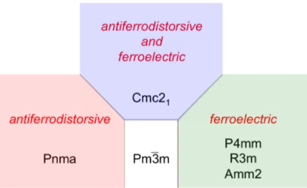
promising candidates in that respect since they present giant SOC.9,10 Moreover, this family of compounds can be found in many different crystal structures. To conduct our survey we decided to start from the highly symmetrical Pm¯3m (n 221) reference phase,52 observed in the high
tem-perature phase of numerous hybrid perovskites.54–57 From this point we follow different phase
transitions (Figure 2). A key point in the observation of a SOC induced spin splitting is the loss of inversion symmetry. Therefore, we take interest in non-centrosymmetric structures, such as fer-roelectric structures. We consider 3D bulk examples belonging to P4mm (n 99), R3m (n 160) and Amm2 (n 38) crystal groups. Then, we consider the case of a temperature induced ferroelec-tric transition in a bulk 2D perovskite. Finally, we investigate the effect of an external elecferroelec-tric field starting with a structure having inversion symmetry that should not be suitable candidates for Rashba or Dresselhaus effect. With the example of CH3NH3PbX3we show that a controllable spin
Figure 2: Phase transitions from Pm¯3m.
Halide organic-inorganic perovskites are hybrid materials and often show important distortions from the ideal octahedron. These deformations are a contributing factor to the different properties of this class of perovskite.58,59 However, if the loss of inversion symmetry is a requirement for the spin splitting, we stress that the loss of too many symmetry operations can lead to an unusable Rashba effect with uncharacteristic spin rotations.
Non-centrosymmetric structures
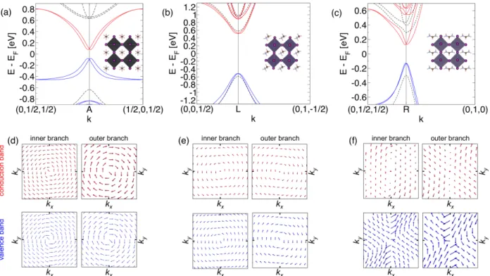
As a first case, we consider the methylammonium lead iodide perovskite CH3NH3PbI3 in the
P4mm crystal group.60 Starting from the Pm¯3m structure, it corresponds to a simple translation
of the ions along the z axis. The resulting structure shows a C4v point group. The C4 axis lies
along the [001] crystallographic direction. Thus, [001] naturally defines the special quantization axisk?,k|| is contained in the plane that can for instance be defined by the two vectorskx=[100]
and ky=[010]. The critical point k0 is the point A (1/2,1/2,1/2). Figure 3-a displays the band
structure of CH3NH3PbI3 calculated with and without SOC in the k|| plane. The SOC has three
major contributions: (i) the gap is greatly reduced, (ii) the conduction band minimum (CBM) and the valence band maximum (VBM) are displaced away from A, (iii) the conduction and valence bands are split away from A. The four resulting bands present similar spin textures (Figure 3-d) with spins orthogonal to the crystal momenta.
Figure 3: Hybrid organic-inorganic halide perovskites crystallized in phases corresponding to a fer-roelectric phase transition from Pm¯3m. (a) Band structure and structure (insert) of CH3NH3PbI3
in the P4mm phase. Blue and red lines stand for the occupied and unoccupied bands for a calcu-lation including SOC, respectively. Black dashed lines are the results without SOC. (b) Same for CH3NH3GeI3in the R3m phase. (c) Same for CH(NH2)2SnI3crystallized in the Amm2 group. (d),
(e) and (f) Spin textures for the inner and outer branches for both occupied and unoccupied bands of CH3NH3PbI3, CH3NH3GeI3and CH(NH2)2SnI3, respectively.
for a C4v symmetry.53 The apparent absence of deviation from the model (Figure 1-b) indicates
weak or vanishing contributions from cubic terms. From the momentum shift kR and the energy
splittingDE we deduce the strength of the Rashba effect lR=DE/(2kR)and find a Rashba
coef-ficient oflCBM
R = 3.76 eV.Å for the conduction band andlRV BM = 3.71 eV.Å for the valence band.
These Rashba splittings are of the same order of magnitude as the largest splittings experimentally observed in bulk materials, e.g. lR = 3.80 eV.Å for BiTeI,26,27 or surface alloys, e.g. lR = 3.05
eV.Å for Bi/Ag(111).31
From the Pm¯3m reference structure simultaneous translations of the ions along the three crys-tallographic axes lead to a R3m structure. The corresponding point symmetry is C3v. In the case
of methylammonium germanium iodide CH3NH3GeI3,60 the C3 quantization axis (k?) is parallel
splitting (k||) contains the [1-10] and [11-2] directions. In Figure 3-b, we plot the band structure following the relevant path around the critical point L (-1/2,1/2,1/2). Once more, splittings are observed for conduction and valence bands. The effect appears more pronounced in the conduc-tion band. The spin textures (Figure 3-e) are again characteristic of a pure Rashba spin splitting as predicted by the symmetry reduction of the k · p Hamiltonian in the case of a C3v point group.53
There is no measurable out-of-plane component of the spin vectors, as it was for CH3NH3PbI3.
We extract again the values oflRand findlRCBM= 0.89 eV.Å,lRV BM = 0.45 eV.Å. These values are
much weaker than those obtained for CH3NH3PbI3, but still sizeable. The lowering of the Rashba
spin splitting is expected as the atomic SOC splitting is much more important for the Pb2+ion than
for Ge2+ (1.75 vs. 0.22 eV).59
CH3NH3GeCl3 also crystallizes in a R3m structure.56 With chlorine, the structure is more
distorted than in the case of iodine (Figure S1-a in Supporting Information). The band structure re-mains similar with a band splitting in conduction and valence bands (Figure S1-b). The difference is quantitative withlCBM
R = 1.18 eV.Å andlRV BM = 0.23 eV.Å. The Rashba effect appears stronger
in the conduction band than in the case of CH3NH3GeI3. The Rashba effect is thus resilient to
important lattice distortions. However, in addition to the expected shape, the spin textures show important out-of-plane components even for small values of the momentum (Figure S1-c and d). This strain-induced alteration of electronic eigenvectors is a detrimental effect that may hinder the definition of purely intricated spin states for device applications (vide infra).
As a final example of ferroelectric structures we investigate CH(NH2)2SnI3 in the Amm2
group.49,61 It corresponds to twin translations of the ions along the x and y directions. The re-sulting point group symmetry is C2v, with the C2 axis in the [011] direction. We plot the band
structure around R (1/2,1/2,1/2) probing the [100] and [01-1] directions. The splitting of bands oc-curs for both the conduction and valence bands. However, the spin textures close to the CBM and VBM for the inner and outer branches (Figure 3-f) are very different from the previous examples, even if no out-of-plane contribution can be extracted. It does not correspond to any of the limiting cases presented in Figure 1. As detailed previously, a system belonging to the C2vsymmetry can
exhibit both Rashba and Dresselhaus terms (Eq. (2)). Using Eq.(3), (10) and the spin orientations for different momentum, we get the relative contributions of both effects: lCBM
D = 2.59 eV.Å and
lCBM
R = 0.50 eV.Å. Our results are in good agreement with previous GW calculations (where the
Rashba and Dresselhaus parameters are computed as DE/kR, accounting for the factor 2
discrep-ancy between their and our results).49The effect is too weak in the valence band and no parameter can be computationally assessed in this case.
Ferroelectric transitions: temperature-controlled Rashba spin
splitting
The ideal reference structure for bulk 2D hybrid perovskites corresponds to the D4hpoint group.62
However, high temperature centrosymmetric crystal phases of 2D hybrid perovskites usually ex-hibit a cell doubling in a plane perpendicular to the stacking axis, associated to antiferrodistorsive tilts of the octahedra. This lattice distortion leads to a reduction of the point group symmetry from D4h to D2h and a BZ folding from the M point at the BZ boundary to theG point at the BZ center.
Such a structure is observed at high temperature for the 2D hybrid perovskite Bz2PbCl4(Bz =
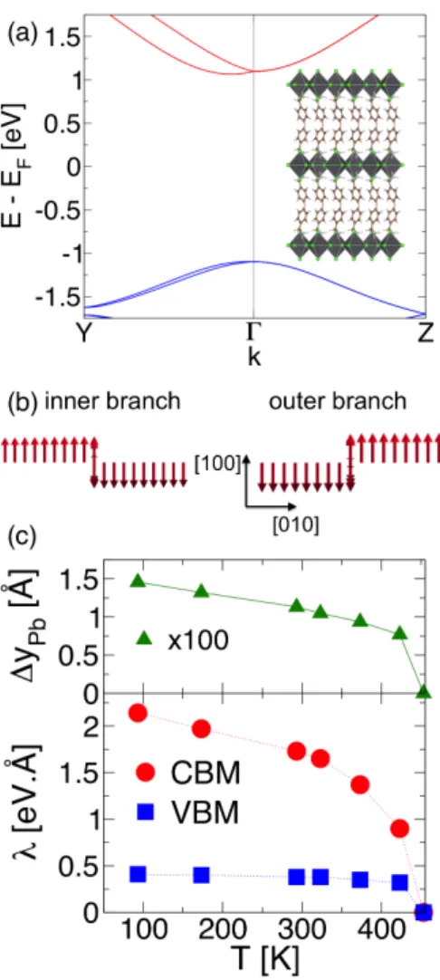
ben-zylammonium),63,64which crystallizes in a Cmca (n 64) centrosymmetric phase.64 The structure
is layered with slabs of single octahedra sandwiched by slabs of organic cations (Figure 4). Below T = 438 K, the crystal undergoes a ferroelectric phase transition to a Cmc21 non-centrosymmetric
structure.
In the low temperature phase, the C2 quantization axis is along the [001] crystallographic
di-rection and thus no spin splitting occurs on theG ! Z path (Figure 4-a). Following the previous scheme,k|| should be defined by [100] and [001]. As [100] corresponds to the stacking direction, there is no dispersion of the bands due to the inorganic part in this direction.9 The spin splitting
can be observed followingG ! Y. This situation notably differs from the Rashba effect in conven-tional semiconductor QW and heterostructures where the stacking and quantization axes coincide.
Therefore, the problem becomes analog to a 1D problem with contributions involving only ky:
H (kx) = lRkysx+lDkysy. (11)
The eigenvalues and eigenvectors become ERD±(ky) = ¯hk 2 y 2m ± q (l2 D+lR2)ky2 (12) Y1D±µ 0 B B @ ⌥qlR ilD l2 R+lD2 ky |ky| 1 1 C C A, (13)
and the spin textures read
hsi±µ 0 B B B B @ ⌥ ky |ky| 0 0 1 C C C C A. (14)
Only one spin component is obtained along the stacking direction. Clearly, there is no differen-tial impact on the observables (band splitting ands expectation values) of the nature Rashba vs. Dresselhaus of the spin splitting. Then, one can notel the effective amplitude:
l = DERD(ky)
2ky . (15)
The band structure calculated for the low-temperature structure (93 K) of Bz2PbCl4(Figure
4-a) shows a large effect on the conduction band (lCBM= 2.14 eV.Å) and much weaker on the valence
band (lV BM = 0.41 eV.Å). The spin textures for both branches of the conduction band (Figure 4-b)
display the expected features with a single component whatever the momentum.
tempera-Figure 4: (a) Band structure of Bz2PbCl4 in the low temperature Cmc21 phase, computed with
SOC. Blue and red bands correspond to occupied and unoccupied bands, respectively. (b) Spin textures for the inner and outer branches of the conduction band. (c) Temperature dependance of the Pb displacement along y (see text) and computed Rashba parameters for the conduction and valence bands.
tures.64The crystal remains in the Cmc2
1group for temperatures from 93 K up to 423 K. The high
temperature structure (453K) presents a Cmca symmetry, i.e. a D2h point group and, therefore,
does not exhibit spin splitting. We compute the electronic structure for each experimental struc-ture and determine the evolution of the Rashba parameter l with temperature (Figure 4-c). The temperature induced variation of the Rashba parameter can be related to the order parameter of the Cmca (D2h) to Cmc21(C2v) ferroelectric phase transition. This order parameter corresponds to the
B1u irreducible representation (IR) of the D2h point group and to a polarization along the C2 axis
the mechanical representations of the Pb and Cl atoms, with a parallel motions of two Pb (or Cl) atoms along the z axis and antiparallel motions along the y axis. The low temperature Cmc21phase
can thus be partly described as a displacive distortion from the Cmca phase with the corresponding atomic displacements in the inorganic layer from their high temperature positions. We shall point out that the phase transition is also related to an order-disorder character in relation with the disor-dered orientations of the organic molecules in the Cmca phase. The splitting in the valence band is weakly affected by the structural changes occurring from 93 to 423 K with alV BM slowly varying
from 0.41 eV.Å to 0.32 eV.Å. On the other hand, the Rashba effect in the conduction bands is stronger This smooth variation is related to the atomic displacement in the low temperature phase. Indeed, the decrease from 2.14 eV.Å to 0.90 eV.Å can be traced back to structural characteristics such as the displacement of Pb atoms along y (Figure 4, S2 and S3).
The effect of octahedron distortions (CH3NH3GeCl3) and of the in-plane and out-of-plane tilts
(Bz2PbCl4) have illustrated the delicate balance of symmetry/asymmetry required to observe a
Rashba effect in this class of hybrid materials. In the following, we consider the case of spin splitting induced by an external electric field.
Field-controlled Rashba spin splitting
In this section, we examine electric field-controlled Rashba splitting starting from 3D hybrid per-ovskites. An electric field applied to the Pm¯3m reference structure correspond to aG4 perturbation, and may lead to one of the three ferroelectric distortion already described in the first part. How-ever, given that the organic cations are dynamically disordered in the Pm¯3m, we perform DFT simulations of this effect for the low-temperature Pnma structure, which corresponds to an anti-ferrodistorsive distortion of the Pm¯3m phase. This centrosymmetric structure is often encountered among hybrid organic-inorganic perovskite56,57,65 and corresponds to the low-temperature phase of CH3NH3PbI3.65 The Pnma space group corresponds to a D2h point symmetry. Therefore, no
Eext is applied, the inversion symmetry is lost and a spin splitting is expected to show up. The
same goes for the cubic Pm¯3m or tetragonal I4/mcm phases.
Control of spin splitting, and thus of the Rashba parameter, by a gate voltage, i.e. an external electric field, has been under intense investigation since the mid-1990s.21–23,32In the early 2000s,
theoretical investigations significantly contributed to rationalize the effect. In particular, tight-binding models have provided essential support to evaluate the Rashba parameter as a function of microscopic quantities.15,66–69 Recently, Kim and coworkers have adapted such models to hybrid organic-inorganic perovskites in the case of non-centrosymmetric structures, but without consid-ering an external electric field.46 Altough the complete description of such models is beyond the
scope of this work, let us recall here that they describe a Rashba parameter that depends linearly on the atomic SOC and on the effective potential gradient, and decreases with an increasing band gap.
In order to apply the electric field, we start from the bulk structure of CH3NH3PbI3 in the
Pnma phase, and construct slabs terminated by the [010] surface, containing ncell octahedra in
the packing direction. Two cases occur: (i) ncell is even (Figure 5-a) and the resulting structure
belongs to the non-centrosymmetric group Pmc21 (n 26) corresponding to the C2v point group,
(ii) ncell is odd (Figure 5-e), and the structure presents a centrosymmetric P21/c (n 14) space
group corresponding to the C2h point group. The consequence of this odd/even effect is illustrated
by the band structures calculated for slabs with ncell= 2 and 3 (Figure 5-b and f) aroundG in both
in-plane directions [100] and [010]. Indeed, no splitting is observed for the conduction and valence bands when ncell = 3, whereas ncell = 2 leads to a small splitting alongG ! X (1/2,0,0). However,
this is not the case when going to thicker slabs: for slabs with ncell 4 no splitting is retrieved in
our calculations.
A spin splitting is observed when applying a transverse electric fieldEext (Figure 5-c and g).
This effect is almost null in the conduction band but can lead tolRof nearly 0.5 eV.Å in the valence
band. Noteworthy, whatever the thickness of the slab, bands close to the gap are not surface states and the splitting is not a difference between up and down faces of the slab. The spin textures of the
Figure 5: Electric field induced spin splitting in slabs of CH3NH3PbI3. The original bulk crystal
group is Pnma. Slabs with even and odd thickness (ncell) exhibit Pmc21 and P21/c symmetry,
respectively. (a) and (e) Structures of slabs of CH3NH3PbI3 with ncell = 2 and 3, respectively.
Pb, I, N, C and H are depicted in gray, purple, blue, brown and white, respectively. (b) and (f) Corresponding band structure computed with SOC. Blue and red bands correspond to occupied and unoccupied band, respectively. A small splitting is observed in the case of ncell = 2. (c)
and (g) Same with the application of an external electric field Eext = 0.075 VÅ 1. A splitting is
observed with corresponding spin textures depicted in (d) and (h) for the valence bands. (i) Rashba parameterlR (eV.Å) as a function of the applied electric field Eext (VÅ 1) for CH3NH3PbI3 (red
circles) and CH3NH3PbBr3(blue squares).
inner and outer branches of the valence band are similar for odd and even cases (Figure 5-d and h) and correspond to Rashba spin splittings.
We monitor the evolution of the valence band Rashba parameter lR with the amplitude of
the applied transverse electric field Eext (Figure 5-i). Let us note that for ncell 7, the bulk gap is
recovered and the Rashba parameter is no longer dependent on the thickness of the slab (Figure S4). In other words, a bulk-like behavior is described. lRowes its increase to two electric field effects:
(i) the induced asymmetry, (ii) the band gap modulation due to the Stark effect that tends to close the gap. We observe a linear dependance oflRwith respect to the external field Eextfor weak fields.
SOC and by the original (no field) band gap of the materials. This can be verified by applying the same procedure to CH3NH3PbBr3 in the same Pnma phase.70 In this way the atomic SOC is
almost constant and only the band gap is modified. It varies from 1.03 eV for CH3NH3PbI3to 1.38
eV for CH3NH3PbBr3 in our DFT+SOC calculations, whose underestimation of semiconductor
band gaps is well-known.10,11,47,71 We find a 28% diminution of lR when replacing I by Br that
is in line with the 33% increase of the band gap. When the field becomes stronger, a bending is observed that might be the related to higher order terms.
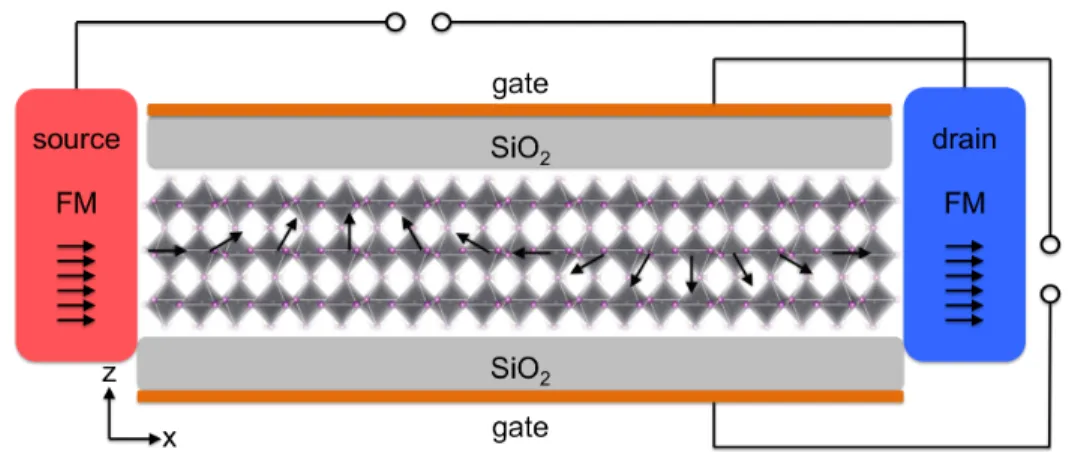
The aspiration for a field-controlled Rashba spin splitting was first motivated by the design of a spin FET following the original scheme proposed by Datta and Das in 1990 (Figure 6).72 In this
setup, the electron spins precess under the influence of the Rashba and/or Dresselhaus coupling. Then, by tuning the amplitude of the effect, one will act on the phase and the electron leaving the source can reach the drain in or out-of-phase. After the very first observations of tunable Rashba splitting,21–23several examples of devices have been produced38,39,73,74or proposed on the basis of theoretical inspections.75,76 More elaborated devices have been proposed based on the same principle, adding a transverse magnetic field to the electric one and using more than one site for SOC effect. In this manner a perfect spin filter can be achieved.77–79
Figure 6: Scheme of a sFET as proposed by Datta and Das72 based on hybrid organic-inorganic
perovskites with a representation of the spin precession from the source to the drain.
Based on our findings, a similar scheme can be proposed using, as an example, the low cost hybrid organic-inorganic perovskite CH3NH3PbI3, in the Pnma structure. Contrary to the previous
splitting (lR=0 eV.Å) when the electric field is switched off, which makes less delicate the tuning
of the source-drain distance and of the amplitude of the transverse field.
Let us consider the case of a ferromagnetic source and drain with magnetizations along +x being also the direction of propagation of the electron. In the semiconductor part of the transistor we find the quantization axis along z, which is the orientation of the gate. The electron is injected with a magnetization along x, i.e. presents a spinor of the form 1/p2(1,1), with an energye. In the case of a Rashba spin splitting, from Eq. (7), the basis on which the spinors are then decomposed is given by |+i =p1 2 0 B @ i 1 1 C A and | i = p1 2 0 B @+i 1 1 C A. (16)
The +x oriented spin is then expressed as
| + xi = 12h(1 + i)|+i + (1 i)| ii. (17) |+i and | i eigenstates propagate with momentum k+ and k given by Eq.(3), with (Figure 1-a)
Dk = k k+= 2m
¯h2lR (18)
and the wavefunction of the propagating electron is given by
Y(x) = 1 2 2 6 4(1 + i)e ik+x p 2 0 B @ i 1 1 C A + (1 i)e ik x p 2 0 B @+i 1 1 C A 3 7 5 (19)
and the expectation value hsi at the distance L is hsi µ 0 B B B B @ cos(Dk.L) 0 sin(Dk.L) 1 C C C C A. (20)
One can see that the spin precesses in the (x,z) plane. To obtain a spin anti-align (off-state) with the magnetization of the drain (Figure 6), the length should be tuned such as
Dk.Loff= (n +12)p, (21)
where n is an integer. And thus,
Loff= (n +12)p ¯h 2
mlR. (22)
If we consider a device with a thickness of 10 nm, then an applied field of 0.0125 V.Å corre-sponds to a gate voltage of 1.25 V and alRof about 0.1 eV.Å. Then, the lengths corresponding to
off-states are 12 nm (n = 0), 36 nm (n = 1), etc.
We stress that these lengths are qualitative estimates. In fact, a quantitative description of spin transport is more complex and entails further developments. For instance, the investigation of spin polarization in these materials remains to be conducted. It requires the use of the full multiband Luttinger Hamiltonian instead of the effective 2 ⇥ 2 one.15,18,80–83 Concurrently, spin relaxation
phenomena, which necessarily occur and would limit the spin diffusion length, should also be taken into account.42Recent experimental data on solution-processed polycrystalline hybrid perovskites
have already shown spin relaxation lifetimes of 7 ps for holes and electrons, suggesting that longer spin diffusion could be reached with crystalline samples.51
Conclusion
Hybrid inorganic-organic perovskite have become extremely popular over the last five years, in the field of photovoltaics. In this respect, they were initially regarded as dyes and, as such, related to organometallic dyes. However, these materials were first considered, in their 2D form, for appli-cations in optoelectronics, and related to conventional semiconductors.6–8 Here we pursue in line
with this and conduct a survey of the Rashba and Dresselhaus effects in these atypical semiconduc-tors. We have recalled the general conditions to observe a Rashba and Dresselhaus spin splittings based on symmetry analysis and k · p expansion. We apply this approach to several examples in non-centrosymmetric structures presenting C4v, C3vand C2vsymmetries. Even for Ge-based
com-pounds we find Rashba parameters of nearly 1 eV.Å, proving that despite the important distortions caused by the organic cation, the SOC effect prevails. By means of a 2D non-centrosymmetric structure, we show how the amplitude of the splitting can be monitored with temperature, as a result of the continuous polarization of the crystal structure from high to low temperatures. Finally we inspect the case of centrosymmetric structure exhibiting a Rashba spin splitting under the in-fluence of a transverse electric field. The possibility to control the spin precession in the material thanks to a gate voltage constitutes the base for a hybrid organic-inorganic perovskite-based spin FET.
Computational details
First-principles calculations are based on DFT as implemented in the SIESTA package.84,85
Cal-culations have been carried out with the GGA functional in the PBE form,86 Troullier-Martins pseudopotentials,87and a basis set of finite-range numerical pseudoatomic orbitals for the valence wave functions.88 Structures relaxation and electronic structure calculations have been done using
a double-z polarized basis sets.88 In our calculations, SOC is taken into account through the
on-site approximation as proposed by Fernández-Seivane et al.89 In all cases, an energy cutoff of 150
the bulk has been relaxed, but no subsequent geometry relaxation has been conducted on slabs. This strategy allows us to stay as close as possible from the bulk behavior of the materials.
We have repeated selected calculations using plane wave basis sets and the projected aug-mented wave method as impleaug-mented in VASP.90,91 We have used the same structures relaxed by
SIESTA with the same exchange and correlation scheme and k-points sampling. The cutoff energy has been chosen between 300 and 500 eV depending on the structure. The results obtained with VASP confirm the main features previously obtained by SIESTA. We have also used the VASP code to obtain the spin textures.
Acknowledgement
This work has been supported by Cellule Energie du CNRS (SOLHYBTRANS Project) and Uni-versity of Rennes 1 (Action Incitative, Défis Scientifiques Emergents 2015). J. E. work is supported by the Fondation d’entreprises banque Populaire de l’Ouest under Grant PEROPHOT 2015. J. E. and C. K. wish to thank R. Winkler for fruitful discussions. We gratefully acknowledge Prof. R.-G. Xiong for providing with Bz2PbCl4crystallographic data.64
Supporting Information Available
Additional results on CH3NH3GeCl3, Bz2PbCl4and CH3NH3PbI3. This material is available free
of charge via the Internet at http://pubs.acs.org/.
References
1. Kojima, A.; Teshima, K.; Shirai, Y.; Miyasaka, T. Organometal halide perovskites as visible-light sensitizers for photovoltaic cells. J. Am. Chem. Soc.2009, 131, 6050.
2. Zhou, H.; Chen, Q.; Li, G.; Luo, S.; Song, T.; Duan, H.-S.; Hong, Z.; You, J.; Liu, Y.; Yang, Y. Interface engineering of highly efficient perovskite solar cells. Science2014, 345, 542.
3. Snaith, H. J. Perovskites: The Emergence of a New Era for Low-Cost, High-Efficiency Solar Cells. J. Phys. Chem. Lett.2013, 4, 3623.
4. Green, M. A.; Ho-Baillie, A.; Snaith, H. J. The emergence of perovskite solar cells. Nature Photon.2014, 8, 506.
5. Grätzel, M. The light and shade of perovskite solar cells. Nature Mater.2014, 13, 838.
6. Mitzi, D. B.; Feild, C. A.; Harrison, W. T. A.; Guloy, A. M. Conducting tin halides with a layered organic-based perovskite structure. Nature1994, 369, 467.
7. Mitzi, D. B.; Wang, S.; Feild, C. A.; Chess, C. A.; Guloy, A. M. Conducting Layered Organic-inorganic Halides Containing <110>-Oriented Perovskite Sheets. Science1995, 267, 1473. 8. Kagan, C. R.; Mitzi, D. B.; Dimitrakopoulos, C. D. Organic-Inorganic Hybrid Materials as
Semiconducting Channels in Thin-Film Field-Effect Transistors. Science1999, 286, 945. 9. Even, J.; Pedesseau, L.; Dupertuis, M.-A.; Jancu, J.-M.; Katan, C. Electronic model for
self-assembled hybrid organic/perovskite semiconductors: Reverse band edge electronic states or-dering and spin-orbit coupling. Phys. Rev. B2012, 86, 205301.
10. Even, J.; Pedesseau, L.; Jancu, J.-M.; Katan, C. Importance of Spin-Orbit Coupling in Hybrid Organic/Inorganic Perovskites for Photovoltaic Applications. J. Phys. Chem. Lett. 2013, 4, 2999.
11. Even, J.; Pedesseau, L.; Jancu, J.-M.; Katan, C. DFT and k.p modelling of the phase transitions of lead and tin halide perovskites for photovoltaic cells. Phys. Status Solidi RRL2014, 8, 31. 12. Dresselhaus, G. Spin-Orbit Coupling Effects in Zinc Blende Structures. Phys. Rev.1955, 100,
580.
13. Rashba, E. I. Properties of semiconductors with an extremum loop. 1. Cyclotron and combi-national resonance in a magnetic field perpendicular to the plane of the loop. Sov. Phys. Solid State1960, 2, 1224.
14. Bychkov, Y. A.; Rashba, E. I. Properties of a 2D electron gas with lifted spectral degeneracy. JETP Lett.1984, 39, 78.
15. Winkler, R. Spin-Orbit Coupling Effects in Two-Dimensional Electron and Hole Systems; Springer, 2003.
16. Dil, J. H. Spin and angle resolved photoemission on non-magnetic low-dimensional systems. J. Phys.: Condens. Matter2009, 21, 403001.
17. Ganichev, S. D.; Golub, L. E. Interplay of Rashba/Dresselhaus spin splittings probed by pho-togalvanic spectroscopy - A review. phys. stat. sol. (b)2014, 251, 1801.
18. Zhang, X.; Liu, Q.; Luo, J.-W.; Freeman, A. J.; Zunger, A. Hidden spin polarization in inversion-symmetric bulk crystals. Nature Phys.2014, 10, 387.
19. Bihlmayer, G.; Rader, O.; Winkler, R. Focus on the Rashba effect. New J. Phys. 2015, 17, 050202.
20. Lommer, G.; Malcher, F.; Rossler, U. Spin splitting in semiconductor heterostructures for B!0. Phys. Rev. Lett. 1988, 60, 728.
21. Nitta, J.; Akazaki, T.; Takayanagi, H.; Enoki, T. Gate Control of Spin-Orbit Interaction in an Inverted In0.53Ga0.47As/In0.52Al0.48As Heterostructure. Phys. Rev. Lett.1997, 78, 1335.
22. Schultz, M.; Heinrichs, F.; Merkt, U.; Colin, T.; Skauli, T.; Løvold, S. Rashba spin splitting in a gated HgTe quantum well. Semicond. Sci. Technol.1996, 11, 1168.
23. Engels, G.; Lange, J.; Schäpers, T.; Lüth, H. Experimental and theoretical approach to spin splitting in modulation-doped InxGa1 xAs/InP quantum wells for B ! 0. Phys. Rev. B 1997,
55, R1958.
24. Balocchi, A.; Amand, T.; Wang, G.; Liu, B. L.; Renucci, P.; Duong, Q. H.; Marie, X. Electric field dependence of the spin relaxation anisotropy in (111) GaAs/AlGaAs quantum wells. New J. Phys.2013, 15, 095016.
25. Wang, G.; Balocchi, A.; Poshakinskiy, A. V.; Zhu, C. R.; Tarasenko, S. A.; Amand, T.; Liu, B. L.; Marie, X. Magnetic field effect on electron spin dynamics in (110) GaAs quan-tum wells. New J. Phys.2014, 16, 045008.
26. Ishizaka, K.; Bahramy, M. S.; Murakawa, H.; Sakano, M.; Shimojima, T.; Sonobe, T.; Koizumi, K.; Shin, S.; Miyahara, H.; Kimura, A. et al. Giant Rashba-type spin splitting in bulk BiTeI. Nature Mater.2011, 10, 521.
27. Eremeev, S. V.; Nechaev, I. A.; Koroteev, Y. M.; Echenique, P. M.; Chulkov, E. V. Ideal Two-Dimensional Electron Systems with a Giant Rashba-Type Spin Splitting in Real Materials: Surfaces of Bismuth Tellurohalides. Phys. Rev. Lett.2012, 108, 246802.
28. Ideue, T.; Checkelsky, J. G.; Bahramy, M. S.; Murakawa, H.; Kaneko, Y.; Nagaosa, N.; Tokura, Y. Pressure variation of Rashba spin splitting toward topological transition in the polar semiconductor BiTeI. Phys. Rev. B2014, 90, 161107(R).
29. LaShell, S.; McDougall, B. A.; Jensen, E. Spin Splitting of an Au(111) Surface State Band Observed with Angle Resolved Photoelectron Spectroscopy. Phys. Rev. Lett.1996, 77, 3419. 30. Koroteev, Y. M.; Bihlmayer, G.; Gayone, J. E.; Chulkov, E. V.; Blügel, S.; Echenique, P. M.;
Hofmann, P. Strong Spin-Orbit Splitting on Bi Surfaces. Phys. Rev. Lett.2004, 93, 046403. 31. Ast, C. R.; Henk, J.; Ernst, A.; Moreschini, L.; Falub, M. C.; Pacilé, D.; Bruno, P.; Kern, K.;
Grioni, M. Giant Spin Splitting through Surface Alloying. Phys. Rev. Lett.2007, 98, 186807. 32. Takayama, A.; Sato, T.; Souma, S.; Oguchi, T.; Takahashi, T. Tunable Spin Polarization in
Bismuth Ultrathin Film on Si(111). Nano Lett.2012, 12, 1776.
33. Bianchi, M.; Hatch, R. C.; Li, Z.; Hofmann, P.; Song, F.; Mi, J.; Iversen, B. B.; Abd El-Fattah, M.; Löptien, P.; Zhou, L. et al. Robust Surface Doping of Bi2Se3 by Rubidium
34. Eremeev, S. V.; Rusinov, I. P.; Nechaev, I. A.; Chulkov, E. V. Rashba split surface states in BiTeBr. New J. Phys.2013, 15, 075015.
35. Santander-Syro, A. F.; Fortuna, F.; Bareille, C.; Rödel, T. C.; Landolt, G.; Plumb, N. C.; Dil, J. H.; Radovi´c, M. Giant spin splitting of the two-dimensional electron gas at the surface of SrTiO3. Nature Mater.2014, 13, 1085.
36. Wang, E.; Tang, P.; Wan, G.; Fedorov, A. V.; Miotkowski, I.; Chen, Y. P.; Duan, W.; Zhou, S. Robust Gapless Surface State and Rashba-Splitting Bands upon Surface Deposition of Mag-netic Cr on Bi2Se3. Nano Lett.2015, 15, 2031.
37. Banerjee, A.; Dogan, F.; Heo, J.; Manchon, A.; Guo, W.; Bhattacharya, P. Spin Relaxation in InGaN Quantum Disks in GaN Nanowires. Nano Lett.2011, 11, 5396.
38. Liang, D.; Gao, X. P. A. Strong Tuning of Rashba Spin-Orbit Interaction in Single InAs Nanowires. Nano Lett.2012, 12, 3263.
39. Zhang, S.; Tang, N.; Jin, W.; Duan, J.; He, X.; Rong, X.; He, C.; Zhang, L.; Qin, X.; Dai, L. et al. Generation of Rashba Spin-Orbit Coupling in CdSe Nanowire by Ionic Liquid Gate. Nano Lett.2015, 15, 1152.
40. Gregg, J. F.; Petej, I.; Jouguelet, E.; Dennis, C. Spin electronics - a review. J. Phys. D: Appl. Phys.2002, 35, R121.
41. Jansen, R. The spin-valve transistor: a review and outlook. J. Phys. D: Appl. Phys.2003, 36, R289.
42. Zuti´c, I.; Fabian, J.; Das Sarma, S. Spintronics: Fundamentals and applications. Rev. Mod. Phys.2004, 76, 323.
44. Sau, J. D.; Lutchyn, R. M.; Tewari, S.; Das Sarma, S. Generic New Platform for Topological Quantum Computation Using Semiconductor Heterostructures. Phys. Rev. Lett. 2010, 104, 040502.
45. Alicea, J.; Oreg, Y.; Refael, G.; von Oppen, F.; Fisher, M. P. A. Non-Abelian statistics and topological quantum information processing in 1D wire networks. Nature Phys.2011, 7, 412. 46. Kim, M.; Im, J.; Freeman, A. J.; Ihm, J.; Jin, H. Switchable S = 1/2 and J = 1/2 Rashba bands
in ferroelectric halide perovskites. Proc. Natl. Acad. Sci. U.S.A.2014, 111, 6900.
47. Brivio, F.; Butler, K. T.; Walsh, A.; van Schilfgaarde, M. Relativistic quasiparticle self-consistent electronic structure of hybrid halide perovskite photovoltaic absorbers. Phys. Rev. B2014, 89, 155204.
48. Amat, A.; Mosconi, E.; Ronca, E.; Quarti, C.; Umari, P.; Nazeeruddin, M. K.; Grätzel, M.; De Angelis, F. Cation-Induced Band-Gap Tuning in Organohalide Perovskites: Interplay of Spin-Orbit Coupling and Octahedra Tilting. Nano Lett.2014, 14, 3608.
49. Stroppa, A.; Di Sante, D.; Barone, P.; Bokdam, M.; Kresse, G.; Franchini, C.; Whangbo, M.-H.; Picozzi, S. Tunable ferroelectric polarization and its interplay with spin-orbit coupling in tin iodide perovskites. Nature Commun.2014, 5, 5900.
50. Kutes, Y.; Ye, L.; Zhou, Y.; Pang, S.; Huey, B. D.; Padture, N. P. Direct Observation of Ferro-electric Domains in Solution-Processed CH3NH3PbI3Perovskite Thin Films. J. Phys. Chem.
Lett.2014, 5, 3335.
51. Giovanni, D.; Ma, H.; Chua, J.; Grätzel, M.; Ramesh, R.; Mhaisalkar, S.; Mathews, N.; Sum, T. C. Highly Spin-Polarized Carrier Dynamics and Ultralarge Photoinduced Magneti-zation in CH3NH3PbI3Perovskite Thin Films. Nano Lett.2015, 15, 1553.
52. Even, J. Pedestrian Guide to Symmetry Properties of the Reference Cubic Structure of 3D All-Inorganic and Hybrid Perovskites. J. Phys. Chem. Lett.2015, 6, 2238.
53. Vajna, S.; Simon, E.; Szilva, A.; Palotas, K.; Ujfalussy, B.; Szunyogh, L. Higher-order contri-butions to the Rashba-Bychkov effect with application to the Bi/Ag(111) surface alloy. Phys. Rev. B2012, 85, 075404.
54. Poglitsch, A.; Weber, D. Dynamic disorder in methylammoniumtrihalogenoplumbates (II) ob-served by millimeter-wave spectroscopy. J. Chem. Phys.1987, 87, 6373.
55. Yamada, K.; Kuranaga, Y.; Ueda, K.; Goto, S.; Okuda, T.; Furukawa, Y. Phase Transition and Electric Conductivity of ASnCl3(A = Cs and CH3NH3). Bull. Chem. Soc. Jpn.1998, 71, 127.
56. Yamada, K.; Mikawa, K.; Okuda, T.; Knight, K. S. Static and dynamic structures of CD3ND3GeCl3 studied by TOF high resolution neutron powder diffraction and solid state
NMR. Dalton Trans.2002, 2112.
57. Chi, L.; Swainson, I.; Cranswick, L.; Her, J.-H.; Stephens, P.; Knop, O. The ordered phase of methylammonium lead chloride CH3ND3PbCl3. J. Solid State Chem.2005, 178, 1376.
58. Filip, M. R.; Eperon, G. E.; Snaith, H. J.; Giustino, F. Steric engineering of metal-halide perovskites with tunable optical band gaps. Nat. Commun.2014, 5, 5757.
59. Katan, C.; Pedesseau, L.; Kepenekian, M.; Rolland, A.; Even, J. Interplay of spin-orbit cou-pling and lattice distortion in metal substituted 3D tri-chloride hybrid perovskites. J. Mater. Chem. A2015, 3, 9232.
60. Stoumpos, C. C.; Frazer, L.; Clark, D. J.; Kim, Y. S.; Rhim, S. H.; Freeman, A. J.; Ketter-son, J. B.; Jang, J. I.; Kanatzidis, M. G. Hybrid Germanium Iodide Perovskite Semiconduc-tors: Active Lone Pairs, Structural Distortions, Direct and Indirect Energy Gaps, and Strong Nonlinear Optical Properties. J. Am. Chem. Soc.2015, 137, 6804.
61. Stoumpos, C. C.; Malliakas, C. D.; Kanatzidis, M. G. Semiconducting Tin and Lead Iodide Perovskites with Organic Cations: Phase Transitions, High Mobilities, and Near-Infrared Pho-toluminescent Properties. Inorg. Chem.2013, 52, 9019.
62. Knutson, J. L.; Martin, J. D.; Mitzi, D. B. Tuning the Band Gap in Hybrid Tin Iodide Per-ovskite Semiconductors Using Structural Templating. Inorg. Chem.2005, 44, 4699.
63. Braun, M.; Frey, W. Crystal structure of bis(benzylammonium) lead tetrachloride, (C7H7NH3)2PbCl4. Z. Kristallogr. New Cryst. Struct.1999, 214, 331.
64. Liao, W.-Q.; Zhang, Y.; Hu, C.-L.; Mao, J.-G.; Ye, H.-Y.; Li, P.-F.; Huang, S. D.; Xiong, R.-G. A lead-halide perovskite molecular ferroelectric semiconductor. Nat. Commun.2015, 6, 7338. 65. Baikie, T.; Fang, Y.; Kadro, J. M.; Schreyer, M.; Wei, F.; Mhaisalkar, S. G.; Grätzel, M.; White, T. J. Synthesis and crystal chemistry of the hybrid perovskite (CH3NH3)PbI3for
solid-state sensitised solar cell applications. J. Mater. Chem. A2013, 1, 5628.
66. Petersen, L.; Hedegård, A simple tight-binding model of spin-orbit splitting of sp-derived surface states. Surf. Sci.2000, 459, 49.
67. Kane, C. L.; Mele, E. J. Quantum Spin Hall Effect in Graphene. Phys. Rev. Lett. 2005, 95, 226801.
68. Konschuh, S.; Gmitra, M.; Fabian, J. Tight-binding theory of the spin-orbit coupling in graphene. Phys. Rev. B2010, 82, 245412.
69. Ast, C. R.; Gierz, I. sp-band tight-binding model for the Bychkov-Rashba effect in a two-dimensional electron system including nearest-neighbor contributions from an electric field. Phys. Rev. B2012, 86, 085105.
70. Swainson, I. P.; Hammond, R. P.; Soullière, C.; Knop, O.; Massa, W. Phase transitions in the perovskite methylammonium lead bromide, CH3ND3PbBr3. J. Solid State Chem.2003, 176,
97.
71. Umari, P.; Mosconi, E.; De Angelis, F. Relativistic GW calculations on CH3NH3PbI3 and
72. Datta, S.; Das, B. Electronic analog of the electrooptic modulator. Appl. Phys. Lett.1990, 56, 665.
73. Yin, C.; Yuan, H.; Wang, X.; Liu, S.; Zhang, S.; Tang, N.; Xu, F.; Chen, Z.; Shimotani, H.; Iwasa, Y. et al. Tunable Surface Electron Spin Splitting with Electric Double-Layer Transistors Based on InN. Nano Lett.2013, 13, 2024.
74. Kim, K.-H.; Um, D.-S.; Lee, H.; Lim, S.; Chang, J.; Koo, H. C.; Oh, M.-W.; Ko, H.; Kim, H. Gate-Controlled Spin-Orbit Interaction in InAs High-Electron Mobility Transistor Layers Epi-taxially Transferred onto Si Substrates. ACS Nano2013, 7, 9106.
75. Di Sante, D.; Barone, P.; Bertacco, R.; Picozzi, S. Electric Control of the Giant Rashba Effect in Bulk GeTe. Adv. Mater.2013, 25, 509.
76. Liu, Q.; Guo, Y.; Freeman, A. J. Tunable Rashba Effect in Two-Dimensional LaOBiS2 Films: Ultrathin Candidates for Spin Field Effect Transistors. Nano Lett.2013, 13, 5264.
77. Citro, R.; Romeo, F.; Marinaro, M. Zero-conductance resonances and spin filtering effects in ring conductors subject to Rashba coupling. Phys. Rev. B2006, 74, 115329.
78. Aharony, A.; Tokura, Y.; Cohen, G. Z.; Entin-Wohlman, O.; Katsumoto, S. Filtering and an-alyzing mobile qubit information via Rashba-Dresselhaus-Aharonov-Bohm interferometers. Phys. Rev. B2011, 84, 035323.
79. Matityahu, S.; Aharony, A.; Entin-Wohlman, O.; Tarucha, S. Spin filtering in a Rashba-Dresselhaus-Aharonov-Bohm double-dot interferometer. New J. Phys.2013, 15, 125017. 80. Winkler, R. Spin polarization of quasi-two-dimensional hole systems. Phys. Rev. B2005, 71,
113307.
81. Winkler, R. Spin orientation and spin precession in inversion-asymmetric quasi-two-dimensional electron systems. Phys. Rev. B2004, 69, 045317.
82. Winkler, R. Spin density matrix of spin-32 hole systems. Phys. Rev. B2004, 70, 125301. 83. Liu, Q.; Zhang, X.; Jin, H.; Lam, K.; Im, J.; Freeman, A. J.; Zunger, A. Search and design of
nonmagnetic centrosymmetric layered crystals with large local spin polarization. Phys. Rev. B 2015, 91, 235204.
84. Soler, J. M.; Artacho, E.; Gale, J. D.; García, A.; Junquera, J.; Ordejón, P.; Sánchez-Portal, D. The SIESTA method for ab initio order-N materials simulation. J. Phys.: Condens. Matter 2002, 14, 2745–2779.
85. Artacho, E.; Anglada, E.; Diéguez, O.; Gale, J. D.; García, A.; Junquera, J.; Martin, R. M.; Ordejón, P.; Pruneda, J. M.; Sánchez-Portal, D. et al. The SIESTA method; developments and applicability. J. Phys.: Condens. Matter2008, 20, 064208.
86. Perdew, J. P.; Burke, K.; Ernzerhof, M. Generalized Gradient Approximation Made Simple. Phys. Rev. Lett.1996, 77, 3865.
87. Troullier, N.; Martins, J. L. EfFicient pseudopotentials for plane-wave calculations. Phys. Rev. B1991, 43, 1993.
88. Artacho, E.; Sánchez-Portal, D.; Ordejón, P.; García, A.; Soler, J. M. Linear-Scaling ab-initio Calculations for Large and Complex Systems. phys. stat. sol. (b)1999, 215, 809.
89. Fernández-Seivane, L.; Oliveira, M. A.; Sanvito, S.; Ferrer, J. On-site approximation for spin-orbit coupling in linear combination of atomic spin-orbitals density functional methods. J. Phys.: Condens. Matter2006, 18, 7999.
90. Kresse, G.; Furthmüller, J. Efficiency of ab-initio total energy calculations for metals and semiconductors using a plane-wave basis set. Comput. Mat. Sci.1996, 6, 15.
91. Kresse, G.; Furthmüller, J. Efficient Iterative Schemes for Ab-Initio Total-Energy Calculations Using a Plane-Wave Basis Set. Phys. Rev. B1996, 54, 11169.