HAL Id: hal-03102361
https://hal.archives-ouvertes.fr/hal-03102361
Submitted on 7 Jan 2021HAL is a multi-disciplinary open access archive for the deposit and dissemination of sci-entific research documents, whether they are pub-lished or not. The documents may come from teaching and research institutions in France or abroad, or from public or private research centers.
L’archive ouverte pluridisciplinaire HAL, est destinée au dépôt et à la diffusion de documents scientifiques de niveau recherche, publiés ou non, émanant des établissements d’enseignement et de recherche français ou étrangers, des laboratoires publics ou privés.
Effective module level encapsulation of CIGS solar cells
with Al2O3 thin film grown by atomic layer deposition
Shan-Ting Zhang, Maxim Guc, Oliver Salomon, Roland Wuerz, Victor
Izquierdo-Roca, Alejandro Pérez-Rodríguez, Friedrich Kessler, Wolfram
Hempel, Thibaud Hildebrandt, Nathanaelle Schneider
To cite this version:
Shan-Ting Zhang, Maxim Guc, Oliver Salomon, Roland Wuerz, Victor Izquierdo-Roca, et al.. Ef-fective module level encapsulation of CIGS solar cells with Al2O3 thin film grown by atomic layer deposition. Solar Energy Materials and Solar Cells, Elsevier, 2021, 222, pp.110914. �10.1016/j.solmat.2020.110914�. �hal-03102361�
Effective module level encapsulation of CIGS solar
cells with Al
2
O
3
thin film grown by atomic layer
deposition
Shan-Ting Zhang a,b,*, Maxim Guc c, Oliver Salomon d, Roland Wuerz d, Victor Izquierdo-Roca c, Alejandro Pérez-Rodríguez c,e, Friedrich Kessler d, Wolfram Hempel d, Thibaud Hildebrandt a,f,
Nathanaelle Schneider a,b
a Institut Photovoltaïque d’Ile-de-France (IPVF), 18 boulevard Thomas Gobert, 91120 Palaiseau,
France
b CNRS, UMR 9006, Institut Photovoltaïque d’Ile-de-France (IPVF), 18 Boulevard Thomas
Gobert, 91120, Palaiseau, France
cCatalonia Institute for Energy Research (IREC), Sant Adrià de Besòs, 08930 Barcelona, Spain
dZentrum für Sonnenenergie- und Wasserstoff-Forschung Baden-Württemberg (ZSW),
Meitnerstraße 1, 70563 Stuttgart, Germany
e IN2UB, Departament d’Electrònica, Universitat de Barcelona, C/ Martí i Franquès 1, 08028
Barcelona, Spain
f EDF R&D, IPVF, 18 boulevard Thomas Gobert, 91120 Palaiseau, France
*Corresponding Author
ABSTRACT: An effective encapsulation solution for flexible CIGS is urgently needed to ensure a competitive market entry of the technology. In this work, we demonstrate the feasibility to effectively encapsulate module-level (10×10 cm2) CIGS/glass solar cells by employing a thin
Al2O3 barrier layer grown by atomic layer deposition (ALD). As determined by a direct
methodology, 10 nm ALD-Al2O3 is proved to be sufficient in preventing electrical degradation of
the Al:ZnO (AZO) window layer upon exposure to damp heat test (DHT) and equally effective to encapsulate 10×10 cm2 CIGS/glass mini-modules by efficient blockage of moisture ingress. CIGS
mini-modules encapsulated by ALD-Al2O3 barrier layer retain an average of 80% and 72% of
initial efficiency after 1000 and 2000 h of DHT, respectively. Whereas unencapsulated modules drop to an average of 67% (1000 h DHT) and 22% (2000 h DHT) of initial efficiency. Thanks to the presence of ALD-Al2O3 barrier layer, less electrical degradation occurred in AZO window
layer and P3 interconnection; also less shunting paths appeared – both led to a lower FF drop in encapsulated CIGS mini-modules. However, an issue of Na migration out of the CIGS layer is observed, which negatively impacts the module stability during DHT.
Keywords: CIGS module, Al2O3, ALD, Raman scattering, damp heat test (DHT), encapsulation
1. Introduction
In the field of photovoltaics (PV), flexible thin film PV technologies have attracted tremendous attention. Compared to their rigid counterpart, flexible thin film solar cells are light weight, allowing a high specific power (kW/kg) which is of particular interest for space applications, and a lower production cost by employing large-scale production techniques enabling high throughput (e.g. roll-to-roll) and a low thermal budget [1]. Furthermore, flexible thin film solar cells can be integrated with elements of various shapes and sizes (such as fabrics, tiles, tents, sails etc.) [2],
thus opening up possibilities for new energy-generating applications, such as the emerging building integrated photovoltaics (BIPV) [3], and vehicle integrated photovoltaics (VIPV) [4]. Among the various flexible PV technologies, copper indium gallium selenide Cu(In,Ga)Se2
(CIGS) solar cell stands out promising. Tiwari et al. have reported a cell efficiency of 20.8% for a CIGS solar cell made on polymer foil [5], which is very close to the record cell efficiency of 23.4% for CIGS on glass substrate [6]. Miasolé has declared to have achieved an efficiency of 18.64% for flexible CIGS at module-level (1.08 m2 aperture) at the end of 2019 [7]. However, to ensure a
cost-competitive market entry for flexible CIGS technology, it is a prerequisite to develop an effective encapsulation solution that can guarantee a module lifetime of >25 years and maintain the flexibility and lightweight of the modules, which still remains a challenge. To evaluate long-term stability without actual field data, it is common practice to expose solar modules to accelerated ageing tests according to the standards of the International Electrotechnical Commission (IEC). One of the most severe tests for thin film modules within the important and widely accepted test protocol based on IEC 61215-2 is the damp heat test (DHT), during which solar modules are exposed to 85 °C and 85% relative humidity (RH) for 1000 hours [8].
In order to retain flexibility, rigid and heavy cover materials (such as glass) are no longer compatible. Instead, polymeric front/back sheets which are lightweight and flexible, are better suited to encapsulate flexible CIGS solar cells. Nevertheless, polymeric materials are generically quite sensitive to moisture ingress [9]. For example, ethylene-vinyl acetate (EVA) copolymers – the most commonly used encapsulant in PV field – are found to decompose when exposed to moisture producing acetic acid [10], which could further degrade the underlying window layer (such as Al:ZnO in CIGS solar cells) [11,12]. The problematic EVA yellowing during outdoor operation (UV and/or humidity exposure) is also a well-known issue [13]. One facile strategy is to
replace the polymeric encapsulant with better H2O-resistant inorganic thin layer between the
polymeric front/back sheet and the flexible CIGS solar cell. The use of inorganic thin layers (such as Al2O3, TiO2, SnO2 etc.) by atomic layer deposition (ALD) has been widely employed in OLED
industry[14,15] and to a less extent in photovoltaics[16–18] as efficient barrier layers. Indeed, ALD is a robust technique enabling pinhole free and conformal deposition of thin films in large-scale with fine control in thickness and material property [19]. Further, ALD can be well adapted for low-temperature deposition and uneven/non-flat substrates [20,21], both of which are of particular interest for flexible CIGS solar cells.
Consequently, ALD grown inorganic barrier layers appear as a promising encapsulation solution for flexible CIGS technology. Among them, Al2O3 is one of the most studied candidates due to its
low water vapor transmission rate (WVTR) of < 10-5 g/m2/day at room temperature for 25 nm
Al2O3 (grown on substrate of polyethylene naphthalate, PEN) [22]. Several large EU projects such
as Nanomend and CLEAN4YIELD have been devoted to developing advanced methodologies to inspect, clean and repair the extremely thin nano-scale barrier layers (e.g. Al2O3). Despite a few
studies on encapsulating CIGS single cells with ALD-grown Al2O3 thin film [23–25], there is
barely report discussing the feasibility of this approach for upscaling (i.e. module level) CIGS devices, which itself presents a critical issue towards commercialization of the technology.
In this work, we encapsulate 10×10 cm2 CIGS/glass mini-modules by ALD-Al
2O3 barrier layers
and discuss the feasibility of this approach for module-level devices against damp heat test. First, a direct methodology is proposed to determine the optimal thickness of ALD-Al2O3, which
conventionally is considered as the minimum thickness required to achieve acceptable WVTR value (e.g. ~6×10⁻⁶ g/m2/day at room temperature as in ref. [24,25]). However, the WVTR
temperature and humidity relevant for the accelerated test of PV modules (i.e. 85 °C and 85% RH), nor is it measured in combination with the polymeric front sheet to be applied in the final solar device. Most of all, the WVTR measurement does not provide any information on the degradation mechanisms of the materials composing the solar cell, whereas the direct methodology employed in this work can reveal this issue. We found out that 10 nm ALD-Al2O3 barrier layer is sufficient
to protect Al:ZnO (AZO) from electrical degradation during DHT by effectively blocking moisture ingress. This barrier of 10 nm ALD-Al2O3 also protects equally efficiently the 10×10 cm2
CIGS/glass mini-modules, particularly at longer exposure time up to 2000 h, when a single layer of ALD-Al2O3 protects the modules in a comparable way as glass-glass encapsulation.
Furthermore, advanced analyses have been performed to reveal the main degradation mechanisms in both unencapsulated and ALD-Al2O3 encapsulated CIGS modules.
2. Experimental Section
2.1 Materials and device fabrication
Al:ZnO (AZO) films of ~ 350 nm were deposited on borosilicate glass substrates by radio-frequency sputtering according to procedures described elsewhere [26]. The top Al2O3 barrier
layers were prepared by atomic layer deposition (ALD) in a BENEQ TFS-200 reactor at deposition temperature Tdep = 160 °C, from trimethyl aluminum (Al(CH3)3, TMA, Optograde, Rohm & Haas)
and deionized water [27]. ALD-Al2O3 of different nominal thicknesses, namely 2, 5, 10, 25, and
80 nm, were tested as barrier layer on AZO/glass. The actual thickness of Al2O3 grown on a control
Si wafer was measured by X-ray reflectivity and is tabulated in Table S1, where it is seen that the measured thickness is fairly close to the nominal thickness. The areal homogeneity of Al2O3
The monolithically interconnected CIGS mini-modules on soda-lime glass (10×10 cm2) were
fabricated in the following way. First, a 500 nm thick molybdenum (Mo) back contact was DC sputtered inline, followed by laser scribing of the Mo back contact (P1), which defines the cell size. The Cu(In,Ga)Se2 absorber was deposited by co-evaporation of the elements in an inline
system (CIS4) at ZSW, which closely resembles an industrial production process. The Mo coated soda-lime glass substrates were transported on carriers (30×30 cm²), starting from an evacuated magazine. A continuous substrate flow was established and transported the carriers at a constant speed through a long vacuum chamber with up to five evaporation units. In these units, self-constructed evaporation sources deposited the elements in a line-shaped profile homogeneously from the top in a typical multi-stage process. In, Ga and Se were deposited in the first unit, followed by Cu and Se in the second unit to achieve a Cu-rich intermediate phase and then In, Ga and Se until the final Cu-poor composition was attained. The substrate heater temperatures were approximately 450 and 650 °C for units one and two, respectively. The 2.2 µm thick CIGS layer grew in approximately 26 minutes. After cooling down a 60 nm thick CdS buffer layer was grown by chemical bath deposition (CBD). After the RF sputtering of a 90 nm thick undoped ZnO layer, the P2 scribe was performed with a mechanical tool. The subsequent Al:ZnO front contact was DC sputtered at a thickness of about 1100 nm. The final P3 patterning step was performed mechanically. Module edge definition was done by sand blasting. Hence, 16 cells were interconnected to one module on a 10×10 cm² glass substrate with an active area of 63.2 cm². All modules were at an efficiency level of >12%. To ensure a low contact resistance after the ALD-Al2O3 deposition and damp heat test, a Ni/Al/Ni layer stack was deposited by electron beam
evaporation onto the ZnO contact bus bars. 2.2 Damp heat test
Damp heat test was performed in a SunEvent SUN/340/S climate chamber from Weiss Umwelttechnik. Modules were first set to 85 °C under dry conditions for 30 min to avoid condensation on the samples. Then the relative humidity (RH) was also increased to 85% RH with the samples staying in the climate chamber until being removed for I-V measurement. The same procedures were then repeated until the total time period of 1000 and 2000 h were reached. 2.3 Characterization techniques
The Bragg-Brentano X-ray diffraction (XRD) patterns were collected on a PANalytical Empyrean equipment (Cu Kα radiation) in the 2theta range of 10°-90°. The sheet resistance on as-grown bare AZO thin film (without Al2O3 barrier layer) was measured using an in-line 4-point
probe (LucasLab Probe 4 apparatus). Raman spectra were measured in a backscattering configuration through the specific probe designed in IREC using the Horiba Jobin Yvon FHR640 monochromator coupled with a CCD camera. The He-Cd gas laser with the 325 nm emission wavelength was used as excitation source. The laser power density was about 10 W/cm2 with the
spot size ~70 µm. These conditions allowed to exclude any thermal effect on the sample surface that could affect the experimental results. All spectra were normalized to the main peak of a single crystalline Si which was imposed to 520 cm-1. For each analyzed sample the Raman spectra were
measured over at least 20 points to control the lateral homogeneity of AZO layers and of CIGS/glass module surfaces.
The current–voltage (I–V) characteristics of CIGS/glass mini-modules were measured at 25 °C under 1000 W/m² simulated AM1.5G illumination (WACOM WXS-90S-5, Voss Electronic GmbH, Kirchheim-Heimstetten, Germany). Before each measurement the samples were light soaked for 10 min at 25 °C under open circuit condition. Such practice has been observed (see
24 h light soaking at 40 °C (the standard long stabilization procedure required by the IEC 61215 protocol). Optical microscopy images were obtained using a Zeiss microscope with a digital camera adapter and a Canon Power shot A620. The dark lock-in thermography (DLIT) measurements were performed using an infrared camera system from Thermosensorik GmbH. High-resolution scanning electron microscopy (SEM) images were taken in an XL30 SFEG system (FEI Deutschland GmbH, Dreieich, Germany). The Time of Flight - Secondary Ion Mass Spectrometry measurements (ToF-SIMS) were carried out in an Iontoff, Münster. A Bi+ liquid ion
source was used as a lateral resolution probe. Sputtered atomic and clustered ions were detected by a time-of-flight detector. An oxygen gas source allowed to dig into deep for recording a depth profile and to increase the sensitivity to measure cations. The analytic area was 300×300 µm2 and
the sputtering area was 450×450 µm2. Alternatively, Cs ions were used to dig into the depth, in
which case the matrix effects are less pronounced compared to sputtering with oxygen. To ensure the validity of comparing the Na SIMS depth profiles of different modules, the Cu signal has been used as a reference signal. The Na depth profiles have been normalized in such a way that the Cu signal of all modules is at the same level.
3. Results and Discussion
3.1 Determination of the optimal thickness of ALD-Al2O3
Extensive studies have shown that for the degradation of CIGS solar cells/modules, both by field exposure and accelerated damp heat test (DHT), the primary failure mode occurs in the top transparent and conductive window layer Al:ZnO (AZO). The sheet resistance R□ of AZO increases due to moisture ingress [28–30], which deteriorates the fill factor (by increasing the series resistance) and thus efficiency of the solar cell [31–35]. As such, by directly monitoring the changes occurring to ALD-Al2O3 encapsulated AZO layers before and after DHT, the optimal
Al2O3 barrier layer thickness required to protect the underlying AZO can be obtained. In parallel,
the degradation mechanism of AZO exposed to DHT can be simultaneously revealed.
Sputtered AZO thin films encapsulated by ALD-Al2O3 barrier layers of 2, 5, 10, 25, and 80 nm
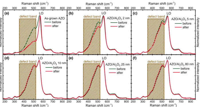
were prepared and exposed to DHT for 1000 h together with an as-grown AZO sample (without ALD-Al2O3 barrier layer). The Raman spectra in Figure 1 record the changes of AZO samples
before and after DHT. Use of ultraviolet (UV 325 nm) excitation wavelength leads to the condition close to resonance for ZnO. Under this excitation condition, an intense LO-like peak located at ~570 cm-1 together with a so-called defect band in the range of 350– 525 cm-1 (shaded in
rectangular) is clearly present in Al doped ZnO thin films. The relative intensity of this defect band has been found to correlate with the resistivity of AZO thin films: the more resistive of the AZO, the lower intensity of this defect band [36,37]. This feature of the defect band is related to the interaction of the phonons with the free electron plasma, otherwise called phonon-plasmon coupling effect [38,39]. Note that additional small intensity peaks observed in the Raman spectra are related to numerous multiphonon modes which become more pronounced in the condition of high doping of ZnO [40].
Figure 1. Raman scattering spectra (averaged over at least 20 points) recorded before (dark
curves) and after (red curves) 1000 h damp heat test (DHT) for (a) as-grown AZO, as well as AZO encapsulated with ALD-Al2O3 barrier layers of (b) 2 nm, (c) 5 nm, (d) 10 nm, (e) 25 nm,
and (f) 80 nm.
A close look on the Raman spectra of the as-grown AZO (without ALD-Al2O3 barrier layer) and
ALD-Al2O3 encapsulated AZO thin films reveals a clear dependence of the degradation of
electrical conductivity of AZO on the thickness of ALD-Al2O3 barrier layer. After DHT the defect
band intensity in the as-grown AZO decreases significantly, suggesting a strong degradation of the electrical properties of AZO film (Figure 1a). Indeed, the sheet resistance R□ of as-grown AZO increased from 33.1 Ω/□ to 62.9 Ω/□ after the DHT. On the other hand, for AZO encapsulated with ALD-Al2O3 barrier layer, one sees that with only 2 nm of Al2O3, the defect band intensity
drops to a much smaller extent (Figure 1b, to compare with Figure 1a). Note that slight increase in the defect band intensity for ALD-Al2O3 encapsulated AZO compared to as-grown AZO before
DHT is likely due to a soft annealing of the AZO during the ALD process (at 160 °C for about 1h, see also Figure S2). Further increasing the Al2O3 thickness to 5 nm leads to less degraded AZO,
200 300 400 500 600 700 800 200 300 400 500 600 700 800 200 300 400 500 600 700 800 200 300 400 500 600 700 800 200 300 400 500 600 700 800 200 300 400 500 600 700 800 As-grown AZO before after (a) Raman shift (cm-1) Normali z ed i nte ns it
y defect band defect band
LO (c) AZO/Al2O3 5 nm before after Normali z ed i nte ns it y Raman shift (cm-1) defect band LO (e) AZO/Al2O3 25 nm before after Raman shift (cm-1) defect band LO (d) AZO/Al2O3 10 nm before after Normali z ed i nte ns it y Raman shift (cm-1) defect band LO (b) AZO/Al2O3 2 nm before after LO Raman shift (cm-1) (f) AZO/Al2O3 80 nm before after Normali z ed i nte ns it y Raman shift (cm-1) defect band LO
as evidenced by the even slower drop in the defect band intensity (Figure 1c). With 10 nm Al2O3,
the defect band intensity remains basically unchanged after DHT (Figure 1d), suggesting that 10 nm Al2O3 appears sufficient to protect the AZO thin films against DHT. As expected, with thicker
Al2O3 of 25 and 80 nm, the defect bands of AZO do not decrease in intensity after DHT. It should
be mentioned that the applied Raman methodology reveals mainly the degradation mechanisms related to the intra-grain degradation, while the inter-grain degradation is not assessed. The measurement of sheet resistance can help to reveal inter-grain degradation, which unfortunately is not feasible due to the presence of highly isolating Al2O3 barrier layer. Nevertheless, the effect of
inter-grain degradation is insignificant for the AZO layers with high crystalline quality, where sharp parallel grain boundaries were found to have minimum effect on the electrical properties of doped ZnO [28–30].
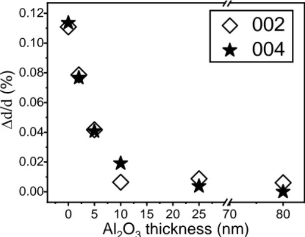
The XRD patterns of the as-grown AZO and AZO encapsulated by ALD-Al2O3 barrier layers
remain almost unchanged before and after DHT, as shown in Figure S3. Since the Al2O3 barrier
layer grown by ALD is amorphous, only the diffraction patterns originating from AZO thin films can be seen. The dominatingly intense diffraction peaks of (002) and (004) suggest that the sputtered AZO thin film is strongly textured. By calculating the interplanar distance d of (002) and (004) planes, it was found that for as-grown AZO both d(002) and d(004) slightly increased after DHT,
implying that water likely penetrates into AZO film and expands the crystal planes. Therefore, the ratio of the relative expansion of d(002) and d(004) after DHT with respect to the values before DHT
is plotted as a function of the thickness of ALD-Al2O3 barrier layer in Figure 2. With increasing
ALD-Al2O3 thickness, the relative expansions of d(002) and d(004) become smaller with respect to
the as-grown AZO sample (i.e. 0 nm Al2O3). With 10 nm Al2O3, the relative interplanar expansion
Al2O3 is sufficient to effectively protect AZO films from water penetration and subsequent
expansion of the crystal planes, consistent with previous Raman observations. Negligible changes in optical transmittance before and after the DHT are observed for AZO thin films without and with Al2O3 barrier layer (see Figure S4), in accordance with the previously published results [35].
Figure 2. The relative expansion ∆d/d of (002) and (004) planes of AZO layers after 1000 h
damp heat test (DHT) as a function of the thickness of ALD-Al2O3 barrier layer. d is the
interplanar distance before DHT and ∆d is the change after DHT. The sample with 0 nm Al2O3
refers to the as-grown AZO.
3.2 Encapsulation of 10×10 cm2 CIGS mini-modules by ALD-Al2O3
In total, 14 CIGS mini-modules on glass (10×10 cm2) were prepared and encapsulated by
ALD-Al2O3 of different thicknesses. Table 1 summarizes the nomenclature of these modules and their
treatments.
Table 1: Summary of 14 CIGS mini-modules on glass (10×10 cm2) and their treatments
Name # modules Remarks
Unencapsulated 4 Annealed in ALD reactor for 1 h 10 nm Al2O3 2 Encapsulated with 10 nm ALD-Al2O3
25 nm Al2O3 4 Encapsulated with 25 nm ALD-Al2O3
80 nm Al2O3 4 Encapsulated with 80 nm ALD-Al2O3 0 5 10 15 20 25 70 80 0.00 0.02 0.04 0.06 0.08 0.10 0.12
002
004
Dd /d ( %) Al2O3 thickness (nm)Since the growth of ALD-Al2O3 barrier layer was carried out at 160 °C for about 1 h (total
duration for the whole ALD-Al2O3 deposition process of all thicknesses considered), the 4
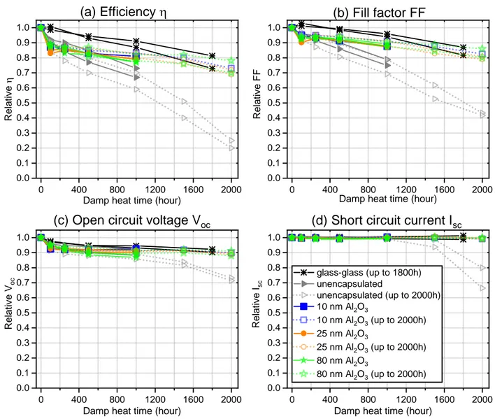
unencapsulated CIGS mini-modules were also annealed in the ALD reactor at 160 °C for around 1h. As such, both unencapsulated and encapsulated mini-modules underwent the same thermal treatment before DHT, making the comparison between the degradation of their performance reasonable. The average initial efficiency of these modules is about 13.3%. The 14 CIGS mini-modules were then placed altogether in a climate chamber and exposed to damp heat test (DHT). In order to monitor the change of optoelectrical properties of the mini-modules, they were removed from the climate chamber after a certain time to perform I-V characteristics. Typical I-V curves at different damp heat hours are summarized in Figure S5 for selected modules. All modules were exposed to DHT for 1000 h as required by IEC 61215-2 and half of the modules were further exposed up to 2000 h. The relative change of efficiency (η), fill factor (FF), open circuit voltage (Voc), and short circuit current (Isc) as a function of damp heat time are summarized in Figure 3.
Here, two as-prepared CIGS mini-modules (without annealing in ALD reactor) were completely encapsulated with a commercial ionomer (Juraplast) without edge sealant and an iron-free glass at 160 °C for 30 min (“glass-glass” encapsulation) and are also included for comparison purpose.
Figure 3. Relative changes of (a) efficiency η, (b) fill factor FF, (c) open circuit voltage Voc, and
(d) short circuit current Isc for 10×10 cm2 unencapsulated CIGS/glass mini-modules and those
encapsulated by ALD-Al2O3 barrier layer (10, 25 and 80 nm as indicated in the figures) as a
function of damp heat time. The modules with up to 2000 h DHT are shown in open symbols. Two as-prepared modules completely encapsulated with “glass-glass” scheme are also included
for comparison purpose. The detailed datapoints are listed exhaustively in Table S2-S5. Up to 1000 h DHT, the efficiency of the unencapsulated CIGS mini-modules drops to an average of 67% of the initial value while those encapsulated with ALD-Al2O3 barrier layers maintain an
average of 80% of the initial efficiency. The glass-glass encapsulated CIGS mini-modules remain about 90% of the initial efficiency. Compared to unencapsulated CIGS mini-modules, less
0 400 800 1200 1600 2000 0.0 0.1 0.2 0.3 0.4 0.5 0.6 0.7 0.8 0.9 1.0 0 400 800 1200 1600 2000 0.0 0.1 0.2 0.3 0.4 0.5 0.6 0.7 0.8 0.9 1.0 0 400 800 1200 1600 2000 0.0 0.1 0.2 0.3 0.4 0.5 0.6 0.7 0.8 0.9 1.0 0 400 800 1200 1600 2000 0.0 0.1 0.2 0.3 0.4 0.5 0.6 0.7 0.8 0.9 1.0 R e la ti ve h
Damp heat time (hour)
glass-glass (up to 1800h) unencapsulated unencapsulated (up to 2000h) 10 nm Al2O3 10 nm Al2O3 (up to 2000h) 25 nm Al2O3 25 nm Al2O3 (up to 2000h) 80 nm Al2O3 80 nm Al2O3 (up to 2000h) (a) Efficiency h
(c) Open circuit voltage Voc
(b) Fill factor FF
(d) Short circuit current Isc
R e la ti ve F F
Damp heat time (hour)
R e la ti ve V oc
Damp heat time (hour)
R e la ti ve Isc
degradation is observed in ALD-Al2O3 encapsulated ones although the efficiency drop is still
higher than the criteria set by IEC 61215-2 (95% initial efficiency after 1000 h). The effectiveness of ALD-Al2O3 encapsulation appears more significant with further exposure up to 2000 h, where
the unencapsulated mini-modules are almost completely degraded (with only ~22% of the initial efficiency remained) and the encapsulated ones still retain ~72% of the initial efficiency. As a matter of fact, with longer (>1000 h) damp heat time, the efficiencies of CIGS mini-modules encapsulated with a single layer of ALD-Al2O3 are fairly comparable to those of glass-glass
encapsulated bench mini-modules (~77% initial efficiency after 1800 h). It is thus reasonable to conclude that ALD-Al2O3 barrier layer is an effective encapsulant for CIGS mini-modules.
As compared to IEC 61215-2, one notices the following main changes up to 1000 h DHT: 1) Isc remains constant for both unencapsulated and ALD-Al2O3 encapsulated mini-modules,
suggesting absence or insignificant changes in the recombination process and interface quality upon exposure to damp heat.
2) FF drops significantly in the first 100 h of DHT, then the drop continues with similar slope for unencapsulated mini-module while for ALD-Al2O3 encapsulated mini-modules the FF drop
becomes much smoother.
3) Voc drops by about 6% in the first 100 h of DHT, then gently decreases down by 10% at 1000
h of DHT for both unencapsulated and ALD-Al2O3 encapsulated mini-modules.
Change in fill factor FF
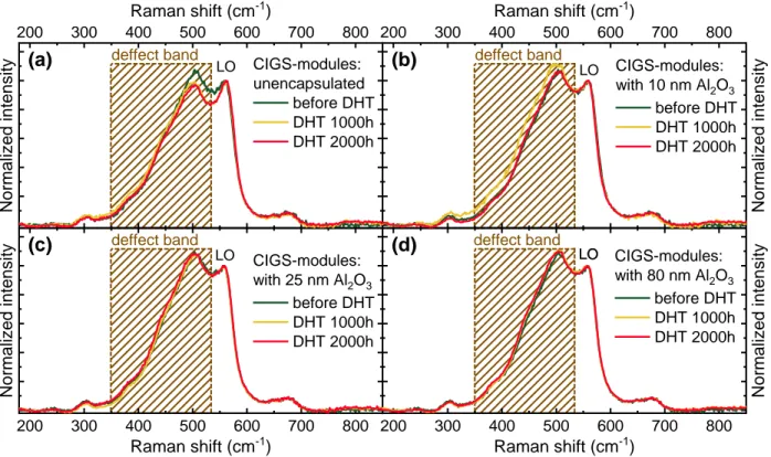
The drop in FF can be either due to increased series resistance or decreased shunt resistance or both. The electrical conductivity loss of the AZO top window layer due to humidity penetration has been observed as one of the primary causes to the increase of series resistance (thus FF drop). In order to probe how the humidity penetration affects the electrical properties of AZO layer,
Raman measurements were performed directly on CIGS mini-modules, as shown in Figure 4. For the unencapsulated module (Figure 4a), the intensity of the defect band decreases after DHT (both 1000 and 2000 h). This indicates a degradation of the conductivity of the AZO layer after damp heat exposure due to severe moisture penetration. On the other hand, for the ALD-Al2O3
encapsulated modules (Figure 4b-d), the defect band does not decrease after DHT. Thanks to the blockage by ALD-Al2O3 barrier layer, less humidity penetrates into encapsulated modules
compared to the unencapsulated ones, thus the AZO window layer retains its conductivity. Nevertheless, as mentioned in the section 3.1, Raman spectroscopy can assess only the intra-grain conductivity, while the inter-grain conductivity is not evaluated. It should be mentioned that the microscopically insignificant decrease of the (inter-grain) conductivity would have a pronounced influence at the module level (e.g. large lateral distance for current transport in AZO layer before reaching the metallic contact), resulting in a perceptible increase of the module’s series resistance. Meanwhile, in modules, a slight reduction in the conductivity of AZO can lead to a significant increase of the contact resistance in P2 interconnection [41–43]. Moreover, the electrical degradation of AZO layer does not seem to vary linearly with damp heat time, as the defect band intensities in the unencapsulated modules are quite similar after 1000 and 2000 h DHT (see Figure
4a). This suggests that the most degradation likely occurs in the first 100 h DHT; after 100 h, the
Figure 4. Raman scattering spectra (averaged over at least 20 points) taken before (dark green
curves) and after 1000 h (yellow curves), 2000 h (red curve) damp heat test (DHT) for (a) unencapsulated CIGS mini-module, as well as CIGS mini-modules encapsulated with ALD-Al2O3
barrier layers of (b) 10 nm, (c) 25 nm, and (d) 80 nm.
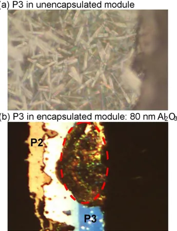
In addition to the electrical degradation of AZO, degradation in the P3 interconnection was also observed. As seen in the optical image in Figure 5a, for the unencapsulated module, the Mo back contact in P3 shows severe degradation accompanied by the formation of needle-like structures. The composition of needles formed on Mo is suggested to be rich of carbonate salts such as Na2CO3 and is indicative of strong oxidation of the Mo back contact upon exposure to humidity
and oxygen [44]. The presence of Na is believed to be migrated from the soda-lime glass substrate. It is clear that in unencapsulated modules, due to humidity penetration, severe degradation in the Mo back contact occurred (at least at the P2/P3 interconnections), which would contribute to an increase in series resistance, resulting in a lowering of FF. In ALD-Al2O3 encapsulated modules,
200 300 400 500 600 700 800 200 300 400 500 600 700 800 200 300 400 500 600 700 800 200 300 400 500 600 700 800 CIGS-modules: unencapsulated before DHT DHT 1000h DHT 2000h deffect band Raman shift (cm-1) Normal iz ed i ntens
ity (a) LO CIGS-modules:
with 10 nm Al2O3 before DHT DHT 1000h DHT 2000h LO deffect band Normal iz ed i ntens ity Raman shift (cm-1) (b) CIGS-modules: with 25 nm Al2O3 before DHT DHT 1000h DHT 2000h LO Normal iz ed i ntens ity Raman shift (cm-1) (c) deffect band LO CIGS-modules: with 80 nm Al2O3 before DHT DHT 1000h DHT 2000h LO Normal iz ed i ntens ity Raman shift (cm-1) (d) deffect band
however, due to less humidity penetration thanks to the presence of the Al2O3 barrier layer, P3 is
only partially degraded without formation of needle-like structure (see Figure 5b).
Figure 5. (a) Optical image of P3 interconnection for unencapsulated CIGS module after 1000 h
DHT where the needle-like structure is seen to form on the Mo back contact, and for (b) 80 nm ALD-Al2O3 encapsulated module where partial degradation (highlighted in dashed red line) in
P3 is seen. Objective, tube and ocular for the microscope image lead to a thousand-fold and forty-fold optical enlargement in (a) and (b), respectively.
On the other hand, the reduction of the shunt resistance can also contribute to FF degradation. In Figure 6, dark lock-in thermography (DLIT) images were taken before and after 100 and 1000 h DHT on an unencapsulated and encapsulated (with 10 nm ALD-Al2O3) CIGS mini-module,
respectively. When current flows through the cell under reverse-biased condition and without illumination, current preferentially flows through locations with low shunt resistance leading to localized heating [45]. These regions appear brighter (i.e. higher temperature due to more heating) in the images taken with an infrared camera. For all analyzed modules, a few bright spots were
visible already before DHT: shunting paths can occur in as-prepared modules due to imperfections in the manufacturing process (e.g. P1/P2/P3 scribing processes for monolithic cell interconnection, holes in the absorber or buffer layer etc.), although its influence on the module performance is negligible. For both the unencapsulated and ALD-Al2O3 encapsulated modules, after only 100 h
DHT, the number of bright spots are fairly similar to that before DHT, suggesting negligible appearance of new shunting paths up to 100 h DHT. For the module encapsulated with 10 nm ALD-Al2O3, the situation remains similar with further increase of DHT time up to 1000 h. The
same applied to the modules encapsulated with 25 and 80 nm ALD-Al2O3 (see Figure S6). For
the unencapsulated module, however, up to 1000 h DHT, a significant number of new shunts appear, most of which are along the patterning lines (P2/P3). The Mo in the P3 line is previously shown to degrade severely with needle formations, which could provide shunting path.
Figure 6. Dark lock-in thermography (DLIT) images taken before, after 100 h and 1000 h
DHT for (a) unencapsulated and (b) 10 nm ALD-Al2O3 encapsulated CIGS mini-modules. The
brighter spots indicate possible shunting paths.
To sum up, for the unencapsulated mini-modules, due to progressive humidity penetration, severe degradations occurred on the top AZO window layer and P3 interconnection (e.g. oxidation of Mo), consequently the conductivity loss in both AZO and Mo layer contribute to series resistance, thus strong reduction of FF occurs at 100 h DHT. After 100 h DHT, the further reduction of FF in the unencapsulated modules up to 1000 h DHT is mainly dominated by the significant appearance of shunting paths (possibly along with continued but slower decrease of the AZO layer conductivity). In contrast, for the encapsulated mini-modules, as ALD-Al2O3 barrier
layer effectively blocks humidity penetration, the conductivity of AZO layer did not show detectable change in Raman spectra at any DHT exposure time. Nevertheless, the inter-grain resistance is likely to increase, resulting in perceptible increase of lateral resistance of AZO layer. Together with partial degradation in P3, both effects result in the FF drop at 100 h DHT, after which the FF drops smoothly due to insignificant shunting contribution accompanied with possible insignificant AZO degradation up to 1000 h. For the glass-glass encapsulated mini-modules, the FF shows negligible drop in the first 100 h DHT suggesting that the humidity penetration is even better slowed down owing to the complete encapsulation stacks. However, with increasing damp heat time, the humidity seems to progressively penetrate into the module, resulting in FF drop comparable to modules encapsulated with a single ALD-Al2O3 layer up to 1000 h DHT.
Change in open circuit voltage Voc
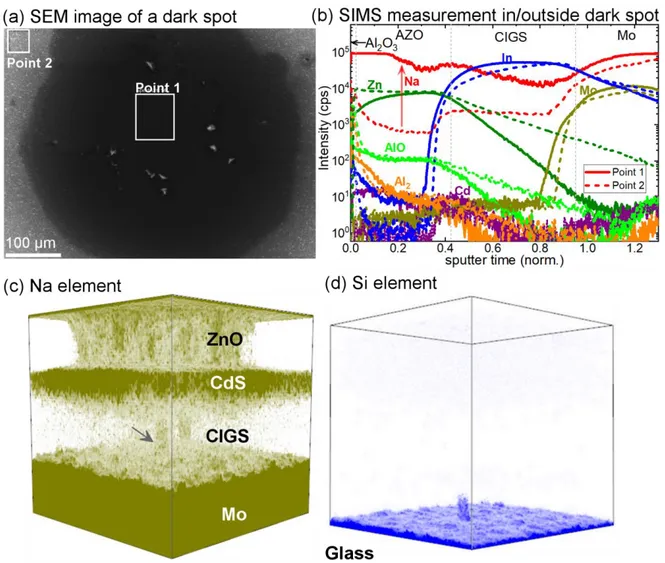
We notice that after DHT, some dark spots as shown in Figure 7a appeared on certain modules, which were even visible to the naked eye in some cases. First examination by EDS (not shown) indicates that the dark spot is rich in Na (for example, on one dark spot about 5.2 at.% Na is
detected while outside the dark spot the Na signal is negligible). Detailed ToF-SIMS measurements in Figure 7b indeed confirm a higher quantity of Na inside such a dark spot. The formation of spots rich in Na was indeed reported to occur in CIGS absorbers exposed to a few hours of damp heat [46], or for several months in ambient atmosphere [35]. Here, inside the dark spot, some additional quantity of Cd is detected in the top AZO layer together with a slight deficiency of Zn and increased Al towards the AZO surface. This suggests that defects, such as segregation of Al and depletion of Zn or thickness non-uniformities, are likely present in the AZO layer, which could originate from imperfections during module manufacturing process. Such defective regions evolved gradually during DHT, and eventually visibly appeared as dark spot. One also notices that after DHT, the AlO signal (at the surface where the ALD-Al2O3 barrier layer
is located) inside the dark spot is lower than that outside the spot, suggesting that the Al2O3 layer
on such a dark spot either becomes thinner or disappears. Unfortunately, in this case it is difficult to tell whether it is due to imperfect ALD-Al2O3 deposition (e.g. pin hole defects [47]) or if the
Al2O3 layer gradually degraded (e.g. delaminated) during the DHT. The Na migration should occur
during the CIGS growth from the glass substrate and it is strongly enhanced at such defective regions (which later evolved into dark spots after DHT). As shown in Figure 7c-d where 3D depth-profile of Na through all layers is obtained on a different dark spot, a “channel” for Na migration is clearly visible in the CIGS layer. We did not observe a hole in the Mo layer where the channel is located (not shown), but the Si signal appears earlier below the channel (see Figure 7d). This could be explained by an inhomogeneity of the composition of glass substrate. It appears that during the growth of the CIGS layer, Na migrates via such channels from the glass through Mo to CIGS and then reaches CdS, resulting in a high Na “channel” in the CIGS layer. Excess of sodium can also harm the absorber [48]. For example, in potential induced degradation experiments where
Na was forced into the absorber by an external applied voltage through the glass, the space charge region was enlarged up to the Mo back contact and the doping density was lowered by the negative external potential. The acceptor concentration decreased, which qualitatively explained a Voc drop.
The formation of dark spots was also observed after high charges through the glass in this publication. Further migration of Na also results in accumulation in the top i-ZnO/AZO window layer. The AZO film inside such dark spots appears less conductive (see the Raman spectra in
Figure S7). One should not be confused with Figure 5 where the Raman spectra were averaged
over more than 20 points, all of which were outside the dark spots. Such dark spots most likely developed from defective regions initially formed during the module manufacturing process in which Na from the soda-lime glass tends to preferentially migrate and accumulate, and eventually become more degraded during DHT.
Figure 7. (a) SEM image showing the dark spot on a 25 nm ALD-Al2O3 encapsulated CIGS
mini-module after 1000 h DHT where the SIMS measurements inside (point 1, solid lines) and outside (point 2, dashed lines) the dark spot are presented in (b), the elements copper, gallium,
selenium and sulphur are omitted for clarity reasons. (c)-(d) 3D depth-profile of Na and Si element (area = 300x300 µm2) as determined from ToF-SIMS measurement on a dark spot of a
10 nm ALD-Al2O3 encapsulated CIGS mini-module. The Si signal originates from the glass
substrate and the position of all the layers are identified as shown in the figure. A “channel” for Na migration (marked by an arrow) is also indicated.
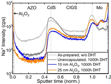
The influence of alkali elements such as Na or K are believed to play an important role in long-term stability of CIGS solar cells [49–52]. As such, the depth profiles of Na (outside of previously mentioned dark spots) were measured on the unencapsulated and ALD-Al2O3 (10 and 25 nm)
encapsulated CIGS mini-modules after 1000 h DHT and are compared to that of an as-prepared module without DHT in Figure 8. In both the unencapsulated and encapsulated CIGS modules, after 1000 h DHT, the Na concentration is reduced in the CIGS layer. It is commonly acknowledged that Na incorporation into the CIGS layer improves the device performance by enhancing the p-type conductivity and passivation of defects, thus improving Voc and FF [53]. In
contrast, the reduction of Na concentration in the CIGS layer observed here results in a lower Voc
and FF.
Figure 8. Na depth-profile as determined from ToF-SIMS measurement on as-prepared
(without DHT), unencapsulated and ALD-Al2O3 (10 and 25 nm) encapsulated CIGS
mini-modules after 1000 h DHT.
Therefore, we propose that the Na migrated out from the CIGS layer during DHT primarily contributes to the decrease in Voc by more or less the same magnitude for both unencapsulated and
ALD-Al2O3 encapsulated CIGS mini-modules: Voc drops most significantly in the first 100 h to
around 94% then slowly decreases to ~90% of the initial value up to 1000 h DHT. The Na migrating out from the CIGS layer is likely also responsible for the Voc drop in glass-glass
encapsulated mini-modules (3 and 6% drop in Voc at 100 h and 1000 h, respectively). Besides the
influence on the Voc, the Na migrating into the Mo accelerates the degradation in the P3
0.0 0.2 0.4 0.6 0.8 1.0 1.2 101 102 103 104 Na + I n te n s it y ( c p s )
Sputter time (norm.)
As-prepared, w/o DHT Unencapsulated, 1000h DHT 10 nm Al2O3, 1000h DHT 25 nm Al2O3, 1000h DHT CdS AZO CIGS Mo Al2O3
interconnection by forming needle-like structures upon exposure to humidity and oxygen, which possibly reduces conductivity of Mo and also provides shunting path, thus decrease the FF – this is the case for unencapsulated modules as in previous discussion. Moreover, the rich Na content in the dark spots lowers the conductivity of AZO, which would locally lead to a higher series resistance, thus is partly responsible for the FF lowering in these modules.
Longer damp heat exposure >1000 h
When further exposing the unencapsulated and ALD-Al2O3 encapsulated CIGS mini-modules
to damp heat from 1000 to 2000 h, the conductivity of AZO layer did not seem to further degrade as evidenced by the Raman spectra (Figure 4). Nevertheless, for unencapsulated modules, one could expect further degradation in P3 interconnection (e.g. Mo back contact) and potential occurrence of more shunting paths as a result of further humidity penetration, which in return severely lowers not only FF but also Voc and Isc. Whereas for mini-modules encapsulated with a
single layer of ALD-Al2O3, only FF drops slightly (due to possibly increased shunting path and
increase of inter-grain resistivity in AZO layer), thus the loss of relative efficiency remains small and is comparable to glass-glass encapsulated modules, suggesting the high promise of using ALD-Al2O3 barrier layer as encapsulation solutions particularly at longer exposure time.
4. Conclusion
To ensure a competitive market entry for flexible CIGS technology, an encapsulation solution is necessary. In this work, we demonstrate the feasibility of employing Al2O3 barrier layers grown
by atomic layer deposition (ALD) to effectively encapsulate module-level CIGS solar cells. Instead of the conventional water vapor transmission rate (WVTR) measurement, we propose a direct method to determine the optimal ALD-Al2O3 barrier layer thickness which simultaneously
ALD-Al2O3 barrier layer as thin as 10 nm is sufficient to protect AZO layers from electrical
degradation upon exposure to 1000 h of damp heat test (DHT). A thin ALD-Al2O3 barrier layer of
10 nm was proved equally effective in encapsulating 10×10 cm2 CIGS/glass mini-modules to
maintain on average 80 and 72% of the initial efficiency after 1000 and 2000 h DHT, respectively. Whereas unencapsulated modules showed stronger degradation, dropping to an average of 67 and 22% of the initial efficiency after 1000 and 2000 h DHT, respectively. Thicker ALD-Al2O3 barrier
layers of 25 and 80 nm behave just as good as 10 nm ALD-Al2O3. Our results clearly suggest that
the ALD-Al2O3 barrier layer works as an effective encapsulant for CIGS modules, particularly at
longer damp heat exposure; instead of using thicker ALD-Al2O3 of >50 nm as in previous works
[23–25], a layer as thin as 10 nm appears sufficient to encapsulate CIGS modules.
As a result of progressive humidity penetration into modules during damp heat exposure, the unencapsulated CIGS/glass mini-modules show severe loss in FF: in the first 100 h DHT, it is mainly caused by increase of series resistance due to conductivity degradation in the AZO window layer and P3 interconnection (e.g. oxidation of Mo back contact) whereas after 100 h the FF loss is dominated by increase in shunting paths. In contrast, for ALD-Al2O3 encapsulated
mini-modules, thanks to the presence of Al2O3 barrier layer, less humidity penetration and thus less FF
degradation are observed. On the other hand, as evidenced by ToF-SIMS measurement, sodium migration out of the CIGS layer during damp heat test negatively affects the performance of modules. The reduction of Na concentration in the CIGS layer after DHT is assumed to lower the hole concentration and hence is responsible for the Voc drop (~10% after 1000 h DHT) in both
unencapsulated and encapsulated modules. Also, the Na migrating into the Mo layer in the P3 interconnection accelerates the degradation of Mo by forming needle-like structures and further
Na migration into the AZO layer results in local reduction of AZO conductivity, both of which would degrade FF.
For the 10×10 cm2 CIGS/glass mini-modules encapsulated with a single layer of ALD-Al 2O3 in
this study, although the efficiency after 1000 h DHT (~20% drop) is still lower than that specified by IEC 61215-2 (≤5% drop), it is promising to note that a thin barrier layer of ALD- Al2O3 protects
the CIGS/glass mini-modules in a comparable manner to the glass-glass encapsulation, particularly at longer damp heat hours of >1000 h. Overall, ALD-Al2O3 barrier layer can be expected to serve
as a promisingly feasible approach to guarantee long-term stability of flexible CIGS solar cells on the module level. Since the barrier is not only extremely thin, but is also applied directly on top of the AZO layer, the flexibility of CIGS modules on thin films or foils is not affected in any way. This could be of great advantage for certain applications.
Supporting Information
Additional supporting information can be found online in the Supporting Information file.
ACKNOWLEDGMENT
This work was supported by the Solar-Era.Net project “Advanced global encapsulation solutions for long term stability in industrial flexible Cu(In,Ga)Se2 photovoltaic technologies” (DURACIS:
Spanish subproject Nr. PCIN-2017-041; French subproject Nr. 1705C0009 (ADEME); German subproject Nr. 0324207). Authors from IREC and the University of Barcelona are supported by the European Regional Development Funds (ERDF, FEDER Programa Competitivitat de Catalunya 2007–2013) and belong to the SEMS (Solar Energy Materials and Systems) Consolidated Research Group of the “Generalitat de Catalunya” (Ref. 2017SGR 862). M.G.
spring Plus fellowship (TECSPR18-1-0048). This work was also partly supported by the French Government in the Programme d’Investissement d’Avenir ANR-IEED-002-01.
REFERENCES
[1] J. Ramanujam, D.M. Bishop, T.K. Todorov, O. Gunawan, J. Rath, R. Nekovei, E. Artegiani, A. Romeo, Flexible CIGS, CdTe and a-Si:H based thin film solar cells: A review, Prog. Mater. Sci. (2019) 100619. https://doi.org/10.1016/j.pmatsci.2019.100619.
[2] M. Pagliaro, R. Ciriminna, G. Palmisano, Flexible Solar Cells, ChemSusChem. 1 (2008) 880–891. https://doi.org/10.1002/cssc.200800127.
[3] M. Pagliaro, R. Ciriminna, G. Palmisano, BIPV: merging the photovoltaic with the construction industry, Prog. Photovolt. Res. Appl. 18 (2010) 61–72. https://doi.org/10.1002/pip.920.
[4] M. Giannouli, P. Yianoulis, Study on the incorporation of photovoltaic systems as an auxiliary power source for hybrid and electric vehicles, Sol. Energy. 86 (2012) 441–451. https://doi.org/10.1016/j.solener.2011.10.019.
[5] R. Carron, S. Nishiwaki, T. Feurer, R. Hertwig, E. Avancini, J. Löckinger, S. Yang, S. Buecheler, A.N. Tiwari, Advanced Alkali Treatments for High‐Efficiency Cu(In,Ga)Se2
Solar Cells on Flexible Substrates, Adv. Energy Mater. 9 (2019) 1900408. https://doi.org/10.1002/aenm.201900408.
[6] https://www.nrel.gov/pv/assets/pdfs/best-research-cell-efficiencies.20191106.pdf. [7]
https://www.pv-magazine.com/2019/11/11/miasole-breaks-its-own-record-for-flexible-cigs/.
[8] International Electrotechnical Commission IEC 61215-2:2016, (2016).
[9] G. Griffini, S. Turri, Polymeric materials for long-term durability of photovoltaic systems, J. Appl. Polym. Sci. 133 (2016) 43080. https://doi.org/10.1002/app.43080.
[10] M.D. Kempe, G.J. Jorgensen, K.M. Terwilliger, T.J. McMahon, C.E. Kennedy, T.T. Borek, Acetic acid production and glass transition concerns with ethylene-vinyl acetate used in photovoltaic devices, Sol. Energy Mater. Sol. Cells. 91 (2007) 315–329. https://doi.org/10.1016/j.solmat.2006.10.009.
[11] D.-W. Lee, W.-J. Cho, J.-K. Song, J.-T. Lee, C.-H. Park, K.-E. Park, H. Lee, Y.-N. Kim, Degradation behaviors of EVA encapsulant and AZO films in Cu(In,Ga)Se2 photovoltaic
modules under accelerated damp heat exposure, Sol. Energy Mater. Sol. Cells. 136 (2015) 135–141. https://doi.org/10.1016/j.solmat.2014.12.036.
[12] D.-W. Lee, W.-J. Cho, J.-K. Song, O.-Y. Kwon, W.-H. Lee, C.-H. Park, K.-E. Park, H. Lee, Y.-N. Kim, Failure analysis of Cu(In,Ga)Se2 photovoltaic modules: degradation mechanism
of Cu(In,Ga)Se2 solar cells under harsh environmental conditions: Failure analysis of CIGS
photovoltaic modules, Prog. Photovolt. Res. Appl. 23 (2015) 829–837. https://doi.org/10.1002/pip.2497.
[13] A.W. Czanderna, F.J. Pern, Encapsulation of PV modules using ethylene vinyl acetate copolymer as a pottant: A critical review, Sol. Energy Mater. Sol. Cells. 43 (1996) 101–181. https://doi.org/10.1016/0927-0248(95)00150-6.
[14] D. Yu, Y.-Q. Yang, Z. Chen, Y. Tao, Y.-F. Liu, Recent progress on thin-film encapsulation technologies for organic electronic devices, Opt. Commun. 362 (2016) 43–49. https://doi.org/10.1016/j.optcom.2015.08.021.
[15] K.L. Jarvis, P.J. Evans, Growth of thin barrier films on flexible polymer substrates by atomic
layer deposition, Thin Solid Films. 624 (2017) 111–135.
https://doi.org/10.1016/j.tsf.2016.12.055.
[16] M.D. Clark, M.L. Jespersen, R.J. Patel, B.J. Leever, Ultra-thin alumina layer encapsulation of bulk heterojunction organic photovoltaics for enhanced device lifetime, Org. Electron. 15 (2014) 1–8. https://doi.org/10.1016/j.orgel.2013.10.014.
[17] M.D. Clark, M.R. Maschmann, R.J. Patel, B.J. Leever, Scratch resistance and durability enhancement of bulk heterojunction organic photovoltaics using ultra-thin alumina layers,
Sol. Energy Mater. Sol. Cells. 128 (2014) 178–183.
https://doi.org/10.1016/j.solmat.2014.05.006.
[18] L. Blunt, D. Robbins, L. Fleming, M. Elrawemi, The Use of Feature Parameters to Asses Barrier Properties of ALD coatings for Flexible PV Substrates, J. Phys. Conf. Ser. 483 (2014) 012011. https://doi.org/10.1088/1742-6596/483/1/012011.
[19] S.M. George, Atomic Layer Deposition: An Overview, Chem. Rev. 110 (2010) 111–131. https://doi.org/10.1021/cr900056b.
[20] M.D. Groner, F.H. Fabreguette, J.W. Elam, S.M. George, Low-Temperature Al2O3 Atomic
Layer Deposition, Chem. Mater. 16 (2004) 639–645. https://doi.org/10.1021/cm0304546. [21] F.J. Ramos, T. Maindron, S. Béchu, A. Rebai, M. Frégnaux, M. Bouttemy, J. Rousset, P.
Schulz, N. Schneider, Versatile perovskite solar cell encapsulation by low-temperature ALD-Al2O3 with long-term stability improvement, Sustain. Energy Fuels. 2 (2018) 2468–2479.
https://doi.org/10.1039/C8SE00282G.
[22] P.F. Carcia, R.S. McLean, M.H. Reilly, M.D. Groner, S.M. George, Ca test of Al2O3 gas
diffusion barriers grown by atomic layer deposition on polymers, Appl. Phys. Lett. 89 (2006) 031915. https://doi.org/10.1063/1.2221912.
[23] P.F. Carcia, R.S. McLean, S. Hegedus, Encapsulation of Cu(InGa)Se2 solar cell with Al2O3
thin-film moisture barrier grown by atomic layer deposition, Sol. Energy Mater. Sol. Cells. 94 (2010) 2375–2378. https://doi.org/10.1016/j.solmat.2010.08.021.
[24] P.F. Carcia, R.S. McLean, S. Hegedus, ALD Moisture Barrier for Cu(InGa)Se2 Solar Cells,
in: ECS Trans, 2010: pp. 237–243. https://doi.org/10.1149/1.3485261.
[25] S. Hegedus, P.F. Carcia, R.S. McLean, B. Culver, Encapsulation of Cu(InGa)Se2 solar cells
with ALD Al2O3 flexible thin-film moisture barrier: Stability under 1000 hour damp heat and
UV exposure, in: 35th IEEE Photovolt. Spec. Conf., IEEE, Honolulu, 2010, pp. 001178– 001183. https://doi.org/10.1109/PVSC.2010.5617334.
[26] D. Hariskos, B. Fuchs, R. Menner, N. Naghavi, C. Hubert, D. Lincot, M. Powalla, The Zn(S,O,OH)/ZnMgO buffer in thin-film Cu(In,Ga)(Se,S)2-based solar cells part II:
Magnetron sputtering of the ZnMgO buffer layer for in-line co-evaporated Cu(In,Ga)Se2
solar cells, Prog. Photovolt. Res. Appl. 17 (2009) 479–488. https://doi.org/10.1002/pip.897. [27] H. Le Tulzo, N. Schneider, D. Lincot, G. Patriarche, F. Donsanti, Impact of the sequence of
precursor introduction on the growth and properties of atomic layer deposited Al-doped ZnO films, J. Vac. Sci. Technol. A. 36 (2018) 041502. https://doi.org/10.1116/1.5030990.
[28] J. Owen, J. Hüpkes, L. Niessen, U. Zastrow, W. Beyer, Damp-Heat Treatment Effects on Sputtered Al-Doped ZnO Films, in 24th Eur. Photovolt. Sol. Energy Conf., Hamburg, 2009,
[29] D. Greiner, N. Papathanasiou, A. Pflug, F. Ruske, R. Klenk, Influence of damp heat on the optical and electrical properties of Al-doped zinc oxide, Thin Solid Films. 517 (2009) 2291– 2294. https://doi.org/10.1016/j.tsf.2008.10.107.
[30] D. Greiner, S.E. Gledhill, Ch. Köble, J. Krammer, R. Klenk, Damp heat stability of Al-doped zinc oxide films on smooth and rough substrates, Thin Solid Films. 520 (2011) 1285–1290. https://doi.org/10.1016/j.tsf.2011.04.190.
[31] J.A. del Cueto, S. Rummel, B. Kroposki, C. Osterwald, A. Anderberg, Stability of CIS/CIGS modules at the outdoor test facility over two decades, in: 33rd IEEE Photovoltaic Spec. Conf., San Diego, 2008, pp. 1–6. https://doi.org/10.1109/PVSC.2008.4922772.
[32] R. Feist, S. Rozeveld, M. Mushrush, R. Haley, B. Lemon, J. Gerbi, B. Nichols, R. Nilsson, T. Richardson, S. Sprague, R. Tesch, S. Torka, C. Wood, S. Wu, S. Yeung, M.T. Bernius, Examination of lifetime-limiting failure mechanisms in CIGSS-based PV minimodules under environmental stress, in: 33rd IEEE Photovoltaic Spec. Conf., San Diego, 2008, pp. 1–5. https://doi.org/10.1109/PVSC.2008.4922579.
[33] D.-W. Lee, O.-Y. Kwon, J.-K. Song, C.-H. Park, K.-E. Park, S.-M. Nam, Y.-N. Kim, Effects of ZnO:Al films on CIGS PV modules degraded under accelerated damp heat, Sol. Energy Mater. Sol. Cells. 105 (2012) 15–20. https://doi.org/10.1016/j.solmat.2012.05.002.
[34] M. Theelen, M. Tomassini, H. Steijvers, Z. Vroon, N. Barreau, M. Zeman, In-situ analysis of the degradation of Cu(In, Ga)Se2 solar cells, in: 39th IEEE Photovolt. Spec. Conf. PVSC,
Tampa,2013, pp. 2047–2051. https://doi.org/10.1109/PVSC.2013.6744875.
[35] M. Theelen, F. Daume, Stability of Cu(In,Ga)Se2 solar cells: A literature review, Sol. Energy.
133 (2016) 586–627. https://doi.org/10.1016/j.solener.2016.04.010.
[36] M. Guc, F. Tsin, J. Rousset, Y.E. Romanyuk, V. Izquierdo-Roca, A. Pérez-Rodríguez, Nondestructive Raman Scattering Assessment of Solution-Processed ZnO-Doped Layers for Photovoltaic Applications, J. Phys. Chem. C. 121 (2017) 3212–3218. https://doi.org/10.1021/acs.jpcc.6b11525.
[37] C. Insignares-Cuello, X. Fontané, Y. Sánchez-González, M. Placidi, C. Broussillou, J. López-García, E. Saucedo, V. Bermúdez, A. Pérez-Rodríguez, V. Izquierdo-Roca, Non-destructive assessment of ZnO:Al window layers in advanced Cu(In,Ga)Se 2 photovoltaic technologies:
ZnO:Al window layers in advanced Cu(In,Ga)Se2 PV technologies, Phys. Status Solidi A.
212 (2015) 56–60. https://doi.org/10.1002/pssa.201431222.
[38] B.B. Varga, Coupling of Plasmons to Polar Phonons in Degenerate Semiconductors, Phys. Rev. 137 (1965) A1896–A1902. https://doi.org/10.1103/PhysRev.137.A1896.
[39] B.H. Bairamov, A. Heinrich, G. Irmer, V.V. Toporov, E. Ziegler, Raman study of the phonon halfwidths and the phonon—plasmon coupling in ZnO, Phys. Status Solidi B. 119 (1983) 227–234. https://doi.org/10.1002/pssb.2221190126.
[40] R. Cuscó, E. Alarcón-Lladó, J. Ibáñez, L. Artús, J. Jiménez, B. Wang, M.J. Callahan, Temperature dependence of Raman scattering in ZnO, Phys. Rev. B. 75 (2007) 165202. https://doi.org/10.1103/PhysRevB.75.165202.
[41] J. Wennerberg, J. Kessler, L. Stolt, Cu(In,Ga)Se2-based thin-film photovoltaic modules
optimized for long-term performance, Sol. Energy Mater. Sol. Cells. 75 (2003) 47–55. https://doi.org/10.1016/S0927-0248(02)00101-0.
[42] J. Klaer, R. Klenk, A. Boden, A. Neisser, C. Kaufmann, R. Scheer, H.-W. Schock, Damp heat stability of chalcopyrite mini-modules: evaluation of specific test structures, in: 31st IEEE Photovolt. Spec. Conf., Lake buena Vista, 2005, pp. 336–339. https://doi.org/10.1109/PVSC.2005.1488137.
[43] P.-O. Westin, P. Neretnieks, M. Edoff, Damp heat degradation of CIGS-based PV Modules, in: 21st Eur. Photovolt. Sol. Energy Conf., Dresden, 2006, pp. 2470–2473.
[44] M. Theelen, K. Polman, M. Tomassini, N. Barreau, H. Steijvers, J. van Berkum, Z. Vroon, M. Zeman, Influence of deposition pressure and selenisation on damp heat degradation of the Cu(In,Ga)Se2 back contact molybdenum, Surf. Coat. Technol. 252 (2014) 157–167.
https://doi.org/10.1016/j.surfcoat.2014.05.001.
[45] D.L. King, J.A. Kratochvil, M.A. Quintana, T.J. McMahon, Applications for infrared imaging equipment in photovoltaic cell, module, and system testing, in: 28th IEEE Photovolt. Spec. Conf., Anchorage, 2000, pp. 1487–1490. https://doi.org/10.1109/PVSC.2000.916175. [46] F.J. Pern, B. Egaas, B. To, C.-S. Jiang, J.V. Li, S. Glynn, C. DeHart, A study on the humidity susceptibility of thin-film CIGS absorber, in: 34th IEEE Photovolt. Spec. Conf. PVSC, Philadelphia, 2009, pp. 000287–000292. https://doi.org/10.1109/PVSC.2009.5411676. [47] M. Elrawemi, L. Blunt, L. Fleming, D. Bird, D. Robbins, F. Sweeney, Modelling water
vapour permeability through atomic layer deposition coated photovoltaic barrier defects, Thin Solid Films. 570 (2014) 101–106. https://doi.org/10.1016/j.tsf.2014.08.042.
[48] O. Salomon, W. Hempel, O. Kiowski, E. Lotter, W. Witte, A. Ferati, A. Schneikart, G. Kaune, R. Schäffler, M. Becker, B. Schröppel, R. Vidal Lorbada, D. Mücke, T. Walter, Influence of Molybdenum Back Contact on the PID Effect for Cu(In,Ga)Se2 Solar Cells,
Coatings. 9 (2019) 794. https://doi.org/10.3390/coatings9120794.
[49] F. Daume, A. Rahm, A. Braun, M. Grundmann, Sodium in the Degradation Process of Cu(in,Ga)Se2 Solar Cells, in: 28th Eur. Photovolt. Sol. Energy Conf. Exhib, Paris, 2013, pp.
2192-2198. https://doi.org/10.4229/28THEUPVSEC2013-3BO.7.3.
[50] F. Daume, S. Puttnins, C. Scheit, H. Zachmann, A. Rahm, A. Braun, M. Grundmann, Damp Heat Treatment of Cu(In,Ga)Se2 Solar Cells with Different Sodium Content, Materials. 6
(2013) 5478–5489. https://doi.org/10.3390/ma6125478.
[51] M. Theelen, N. Barreau, F. Daume, H. Steijvers, V. Hans, A. Liakopoulou, Z. Vroon, M. Zeman, Accelerated performance degradation of CIGS solar cell determined by in-situ monitoring, in: SPIE Solar Energy + Technology, San Diego, 2014, p. 91790I. https://doi.org/10.1117/12.2059951.
[52] M. Theelen, N. Barreau, V. Hans, H. Steijvers, Z. Vroon, M. Zeman, Degradation of CIGS solar cells due to the migration of alkali-elements, in: 42nd Photovolt. Spec. Conf. PVSC, New Orleans, 2015, pp. 1–6. https://doi.org/10.1109/PVSC.2015.7355776.
[53] F. Pianezzi, P. Reinhard, A. Chirilă, B. Bissig, S. Nishiwaki, S. Buecheler, A.N. Tiwari, Unveiling the effects of post-deposition treatment with different alkaline elements on the electronic properties of CIGS thin film solar cells, Phys. Chem. Chem. Phys. 16 (2014) 8843. https://doi.org/10.1039/c4cp00614c.