HAL Id: hal-00283405
https://hal.archives-ouvertes.fr/hal-00283405v5
Submitted on 19 Feb 2010
HAL is a multi-disciplinary open access
archive for the deposit and dissemination of
sci-entific research documents, whether they are
pub-lished or not. The documents may come from
teaching and research institutions in France or
L’archive ouverte pluridisciplinaire HAL, est
destinée au dépôt et à la diffusion de documents
scientifiques de niveau recherche, publiés ou non,
émanant des établissements d’enseignement et de
recherche français ou étrangers, des laboratoires
Security Evaluation of a Balanced Quasi-Delay
Insensitive Library (SecLib)
Sylvain Guilley, Florent Flament, Yves Mathieu, Renaud Pacalet
To cite this version:
Sylvain Guilley, Florent Flament, Yves Mathieu, Renaud Pacalet. Security Evaluation of a Balanced
Quasi-Delay Insensitive Library (SecLib). Conference on Design of Circuits and Integrated Systems,
Nov 2008, Grenoble, France. 6 p., ISBN: 978-2-84813-124-5. �hal-00283405v5�
Security Evaluation of a Balanced Quasi-Delay Insensitive
Library (SecLib)
Sylvain GUILLEY, Florent FLAMENT, Yves MATHIEU, Renaud PACALET
Institut TELECOM — TELECOM ParisTech, CNRS LTCI (UMR 5141)
D´epartement COMELEC, 46 rue Barrault, 75 634 PARIS Cedex 13, FRANCE
Abstract
This article presents a library of cells enabling the realization of constant-power cryptoprocessors, na-tively protected against side-channel attacks. The proposed methodology uses a full-custom balanced quasi-delay insensitive (QDI) cell library, called “SecLib”. It is suitable for a shielded routing method derived from the “backend duplication”, using legacy CAD tools for the backend steps. The discussion is oriented towards the explicitation of topological constraints encountered in highly secure designs. We discuss the impact of intra-die techno-logical mismatch on the security of SecLib.
Keywords: Standard cells design, power-constant logic, side-channel attacks mitigation, transistors mismatch, Monte-Carlo simulation.
1
Introduction
Side-channel attacks are a threat to the security of any electronic device. The seminal article of Paul Kocher [8] introduced several attacks, such as the SPA and especially the DPA, that can defeat cryp-toprocessors, whatever the length of the keys. The vulnerability has been identified as an information leakage at the bit-level. Some high-level counter-measures against the DPA, such as duplicating [3] or masking [1], have been put forward. However, given the complexity of the underlying hardware, these solutions can be defeated by exploiting sub-tle non-logical phenomena, such as glitches [10].
Consequently, many ad hoc secured logic styles have been put forward. In the embedded secu-rity community, the so-called DPL (Dual-rail with
Pre-charge Logic) family is overwhelmingly consen-sual. The DPL basically divide into two categories: “power-constant” and “masked-power ” styles. In this paper, we investigate the feasibility of imple-menting optimally secured unmasked logic.
The rest of the paper is organized as follows. The specifications of the balanced QDI secured library “SecLib” is recalled in Sec. 2. Then, the layout challenges of the secured logical gates design are dealt with in Sec. 3. Finally, Sec. 4 concludes the paper and provides some perspectives. The appen-dices A and B describe the derivation of SecLib gates respectively from a template in GDS2 to build the final gate layout and from a template in VHDL to build the final simulation model.
2
Specifications of SecLib
As the “SecLib” cell library is already extensively described by Guilley et al. in [14], only the promi-nent features are recalled in this section.
SecLib is intended to be compatible, in terms of placement sites, with standard cells. This inter-operability enables to reuse legacy cells for non-functional instances. SecLib, like other DPL li-braries tailored for highly secured implementations, features security counter-measures at various levels: protocol, architecture, backend.
At the protocol level, a four-phase protocol en-ables to divide the computations into two steps: the computation proper and the precharge of the netlist. The first step consists in the computation of one iteration, while the second re-initializes all the nets so that the circuit is ready to start a new computation afresh, for instance with all the nets in a same electrical state.
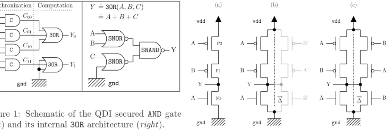
Synchronization C00 C01 C10 C11 C C C C A0 B0 A0 B1 A1 B0 A1 B1 3OR Y0 3OR Y1 Computation gnd Y gnd C B A SNOR SNOR SNAND Y = 3OR(A, B, C). . = A + B + C
Figure 1: Schematic of the QDI secured AND gate (left) and its internal 3OR architecture (right).
Additionally, most secured cells rely on a dual-rail encoding: every logical bit is in fact carried by two wires. Many representations exist; however, a common one consists simply in associating the value false (0) to a wire and the value true (1) to the other. The rationale is to make any transition on the two wires indiscernible.
In dual-rail, every Boolean variable A is repre-sented by a couple of two wires (A0, A1); when A
is valid, A = 0 ⇔ (A0, A1) = (1, 0) and A = 1 ⇔
(A0, A1) = (0, 1). When A is invalid, A0 = A1.
SecLib is optimized for A0= A1= 0.
The overall architecture of a representative Se-cLib gate (Fig. 1) is classical to the QDI logic [6]. The inputs synchronization disables anticipated evaluation. The gate timing is thus uncondi-tional to the data. This feature protects the gate against the signature differences of unsyn-chronized DPL caused by variations of input de-lay time [13]. the inputs configuration decoding (A, B) 7→ (C00, C01, C10, C11) is well suited for an
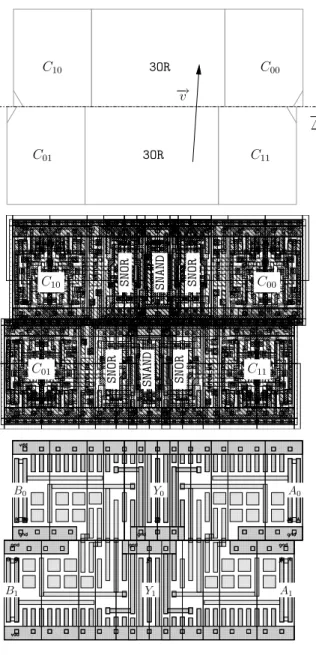
indiscernible processing. Notice that, for unbal-anced functions, the computation part is forced to be symmetric by the use of dummy gates (cf. Fig. 1 schematic on the right). SecLib is close to the logic described in this patent [2]; however, as shown in the sequel, SecLib is much easier to design and to dimension electrically due to the absence of bidi-rectional signals. A B A Y vdd gnd P2 P1 N1 B’ A B A gnd vdd A’ B’ Y − → ∆ B A B A B A gnd vdd Y − → ∆ (a) (b) (c)
Figure 2: Transistor-level schematic of a SNOR gate.
3
Layout of SecLib
3.1
Topological Issues Encountered
in the Layout of SecLib
This section analyzes topological issues met when designing a library of dual-rail secured cells. It de-tails the layout requirements arising from the true ↔ false symmetry need. The layout issues can be circumvented to the sole SecLib instances, since non-functional gates (based on standard cells) do not leak any information. All layouts are realized in a 130 nanometers technology.
The structure of a balanced NOR (called SNOR, for Secured NOR) is shown in Fig. 2(c). The layout challenge consists in porting the symmetry from the schematic to the masks. The basic steps are illus-trated in Fig. 2. First of all, an half-gate is designed (a). Then, two halves are instantiated, one in reg-ular orientation R0, and the other in the mirrored orientation MY (b). This transformation allows for respect of an axial symmetry (the axis is denoted −
→
∆.) The last step, (b) → (c), consists in the inner routing. It raises a topological problem, illustrated in Fig. 3. It is impossible to connect the couples (A, A′) and (B, B′) without a short-circuit, which
results in a functionally invalid solution. This con-cern is not specific to SecLib cells, but indeed in-herent to any geometrical balancing strategy.
An approximation is provided with in Fig. 4. Minimum sized polysilicium segments (130 nm × 180 nm), pointed out by arrows, connect the oppo-site nets: they are selected in Fig. 4 (c). Those four
A B B′ A′ − → ∆ A B B′ A′ − → ∆ short-circuit! Solution (inappropriate) Problem: connect (A,A′) & (B, B′)
Figure 3: −→∆-symmetry topological problem (left); invalid solution (right).
MY
R0
R0
Figure 4: Construction of a quasi-symmetric SNOR gate layout (cf. corresponding schematic in Fig. 2).
segments constitute the sole symmetry violation. The symmetrization methods presented above share the good property that transistors are paired in the same direction. This reduces the devices mis-matches in case of mask misalignments during the manufacturing.
3.2
Gate Cocooning
A good cells library is geared towards the routabil-ity: the minimum number of metal layers must be used for the internal interconnections. In SecLib, only metals 1 and 2 are reserved for inner routing. At the backend level, the decoupling between the computing logic and the routing resources is achieved thanks to an imprisonment of the
transis-Figure 5: Illustration of the M2 cage, on a D-flip-flop. D and Q pins are made available respectively on the left and right sides of the cell.
tors and the local interconnect in a gnd/vdd cage. The power/ground cage, illustrated in Fig. 5, also provides two interesting benefits. First of all, the cell is a cocoon, where the computation takes place confidentially. The symmetry violation between the cell (axial symmetry, hence odd ) and the rout-ing (translation, hence even [14]) is thus minimized. Second, the cage is very convenient to connect the cell to the power and ground global nets. In Fig. 5, the metal 2 pins (positive clock CP, input D, output Q, ground gnd and power vdd) are in bright cyan ( ), whereas obstructions for local interconnect are in low-intensity cyan ( ).
3.3
SecLib Gates Interfaces
The position and the shape of the pins is an impor-tant issue: in order to be visible from a differential pair, the pins must often be larger than expected. For instance, to comply with the “backend dupli-cation” routing method [5], the pins must respect a vertical symmetry, which increases their extension. This constraint arises from the conjunction of the two symmetries:
1. translation T−→v by a vector −→v for the routing
(upper constraint) and
2. glide reflection S−→∆ around an axis −→∆ for the
cell two halves (lower constraint),
that must be met concomitantly by the pins, be-cause they constitute the interface between the two symmetries domains. More formally, if pinF (resp. pinT) is the set of points from the floorplan (i.e.
pinF pinT − →v − → ∆ pinF pinT − →v − → ∆ −1 2 − →v − → ∆ +1 2 − →v ⇔
Figure 6: Translation T−→v and reflection S−→∆
sym-metries to be met by dual pins.
in R2) that belong to the false (resp. true) pin,
then the symmetries impose that: (
pinF = T+−→v(pinT) (routing)
pinF = T+vX−e→
X ◦ S−→∆(pinT) (cell)
and reciprocally, that: (
pinT = T−−→v(pinF) (routing)
pinT = T−vX−e→X ◦ S−→∆(pinF) (cell)
The second constraint can be simplified as the fol-lowing local constraints:
(pinF = S−→∆ +1 2vY−e→Y
(pinF) (pinF symmetry) pinT = S→−∆ −1
2vY−e→Y(pinT) (pinT symmetry) The proof is given below for pinT (the demon-stration for pinF is much similar):
∀(x, y) ∈ pinT, (x′, y′) = (x − vX, y− vY) ∈ pinF,
thus (x′′, y′′) = (x′+ vX,2 · ∆Y − y′) =
(x, 2 · (∆Y −12vY) − y) ∈ pinT .
Figure 6 illustrates this “symmetry transportation” result.
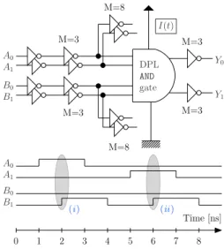
Whenever possible, the pins are placed on the cell right and/or left sides so that two neighbor cells can be routed directly in metal 2. These recommenda-tions are applied on SecLib gates, as shown on the example of the SecLib AND instance in Fig. 7.
The layout of other 2-input gates can be transposed straightforwardly from that of the AND gate. For instance, the family (A, B) 7→ { ¯A · ¯B, ¯A · B, A · ¯B, A · B} can be drawn based on the same template, specialized by the ad-dition of vias at the relevant places [4]. Some details are provided in appendices A and B. SecLib cells are asynchronous, hence hazard-free: arbitrary Boolean functions can be implemented. Other non-synchronizing logics must restrict themselves to
C10 C01 C00 C11 − → ∆ 3OR 3OR − →v C10 C01 C00 S N O R S N A N D S N O R S N O R S N A N D S N O R C11 A1 A0 Y0 Y1 B0 B1
Figure 7: SecLib two-input AND gate floorplan (top), structure (middle) and interface (bottom).
positive functions in order not to generate and not to propagate data-dependent glitches. The aver-age density of SecLib is 545 527 transistors/mm2,
versus 766 586 for the standard cells.
3.4
Mismatch Impact on Gates
Bal-ancedness
In deep sub-micron technologies, the electrical pa-rameters are subject to local mismatches, that po-tentially wreak havoc the symmetry of secured gates. The term mismatch is defined as the elec-trical parameter deviation between identically de-signed components. It is customarily used in analog devices to predict their unbalancedness. The mis-match results from electrical fluctuations induced by nanoscopic variations in physical quantities.
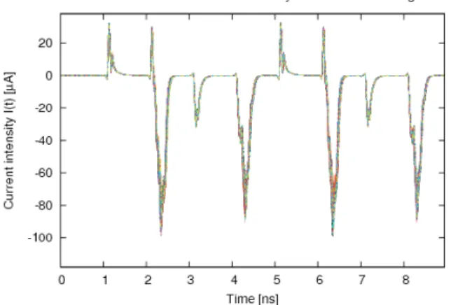
A study on the mismatch in a differential inter-connect network is carried out in [7]. This sub-section accounts for the threshold voltage mismatch simulation on the instant and average current con-sumed by secured DPL gates. Both SecLib and WDDL [16] logics are studied, based on the exam-ple of an AND gate. The comparison is made be-tween those two logic styles because they both use “full-amplitude” signals (from gnd to vdd volts – as the standard cells provided in founders design kits), which would not be the case for SABL [15] for in-stance. The testbench is depicted in Fig. 8. The en-vironment is comprised of unitary inverters, of var-ious multiplicities (M=3 or M=8): these values are chosen because they are representative of typical gates neighborhood. The DPL gate is powered by a separate supply, whose current I(t) is extracted. Transistors are provided in 130 nm technology with mismatch models based on Pelgrom’s linear char-acterization [11]. The Monte-Carlo option of elec-trical simulators is used to launch 500 simulations. The waveforms are represented in Fig. 9 for SecLib and WDDL logics.
The relative difference of the instant current I(t) and of the integrated currentR I(t) dt over the tran-sition length are computed between: (i )the tran-sition A = 0, B : 0 → 1, and (ii ) the transition A= 1, B : 0 → 1. This relative difference between these two events is chosen because it is represen-tative of the average unbalancedness that an at-tacker might exploit. The results are summarized in Tab. 1 in the form: “mean ± standard devia-tion”, expressed in percent.
A0 A1 B0 B1 M=3 0 1 2 3 4 5 6 7 8 Time [ns] M=3 M=3 B1 B0 A1 A0 I(t) DPL AND gate M=3 Y0 Y1 M=8 M=8 (i ) (ii )
Figure 8: SPICE testbench for DPL gates instant current I(t) extraction.
Table 1: Relative difference of the maximum and the integrated current consumed by two DPL gates.
SecLib WDDL
max I(t) (−1.01 ± 5.46) % (−0.36 ± 4.87) % R I(t) dt (+0.01 ± 0.33) % (+1.63 ± 0.22) %
Figure 9: Monte-Carlo simulation results for SecLib (top) and WDDL (bottom).
The dispersion is important (about 5 %) on the maximum current peak amplitude. This figure is trustworthy, since commensurate with empiri-cal estimations carried out on a similar technology (90 nm instead of 130 nm) [12]. The mean relative difference is masked in the standard deviation for both SecLib and WDDL. The standard deviation is greater for SecLib, because the gates belonging to this library are comprised of more transistors than WDDL ones. The statistics on the average current relative difference show that:
• SecLib is more balanced than WDDL (| + 0.01| % versus | + 1.63| %),
• the mismatch is the overwhelming source of unbalancedness for SecLib, because the stan-dard deviation is much greater than the mean (0.33 % ≫ | + 0.01| %),
• the structural unbalancedness of WDDL is the principal cause of its unbalancedness (0.22 % ≪ | + 1.63| %).
The “integrated current” metric is believed to be the most representative of measurements that an attacker might realize concretely: as a matter of fact, every measurement is low-passed filtered, because of the chip power grid and of the on-package decoupling capacitances [9, p. 33]. In con-clusion, simulations tend to show that, from the pure computational standpoint, the level of security of SecLib logic is limited by the mismatch, while WDDL is still limited by its intrinsic dissymmetry.
4
Conclusion & Perspectives
This paper revisits the design of statically secured cells suitable for constant-power custom crypto-graphic ICs. Most previously proposed gates are vulnerable to a power attack exploiting the inputs skew. Therefore, this article focuses on a logic style (SecLib) in which gates inputs are systematically resynchronized. A method to port the symmetry constraints from the schematic to the layout is ex-plicited. We emphasize the topological issues raised by the symmetric routing constraints. The question of the positions of the pins is extensively discussed. This issue is indeed crucial since it allows the gates to support balanced differential routing. The paper
concludes positively on the feasibility of industrial-strength secured cells libraries. One strong contri-bution of this paper is to show that secured logics based on standard cells, such as WDDL, are lim-ited by the unbalanced design, but that the bal-ancedness of SecLib is limited only by the intra-die technological mismatch.
Future works will focus on the study of sequential gates (such as memory elements) and of complex circuits (comprised of more than one single gate).
References
[1] M. Akkar and C. Giraud. An Implementation of DES and AES secure against Some Attacks. In Springer-Verlag, editor, Proc. of CHES’01, volume 2162, pages 309–318, 2001.
[2] Lo¨ıc Duflot, Philippe Le Moigne, and Fabien Ger-main. Device Forming a Logic Gate for Minimizing
the Differences in Electrical or Electromagnetic
Behavior in an Integrated Circuit
Manipulat-ing a Secret, November 9 2006. Patent from
the Etat Francais,´ repr´esent´e par le secr´etariat
g´en´eral de la d´efense nationale, WO/2006/117391,
http://www.wipo.int/pctdb/en/wo.jsp?WO=2006117391. [3] Louis Goubin and Jacques Patarin. DES and
Differen-tial Power Analysis (The “Duplication” Method). In
CHES, volume 1965 of LNCS, pages 158–172, 1999.
[4] Sylvain Guilley. Geometrical counter-measures
against side-channel attacks. PhD thesis, GET / ENST, CNRS LTCI (UMR 5141), january 2007. http://pastel.paristech.org/2562/01/phd.pdf. [5] Sylvain Guilley, Philippe Hoogvorst, Yves Mathieu,
and Renaud Pacalet. The “Backend Duplication”
Method. In LNCS, editor, CHES, volume 3659, pages 383–397, August 2005. Edinburgh, Scotland, UK. [6] Sylvain Guilley, Philippe Hoogvorst, Yves Mathieu,
Renaud Pacalet, and Jean Provost. CMOS
Struc-tures Suitable for Secured Hardware. In Proceedings of
DATE’04 – Volume 2, pages 1414–1415. IEEE
Com-puter Society, February 2004. Paris, France. DOI:
10.1109/DATE.2004.1269113.
[7] Makoto Ikeda, Hiroshi Yamauchi, and Kunihiro Asada. Tamper Resistivity Analysis for Nano-meter LSI with Process Variations. In ICECS, pages 387–390, 2006.
[8] P. Kocher, J. Jaffe, and B. Jun. Differential
Power Analysis: Leaking Secrets. In Proceedings of
CRYPTO’99, volume 1666 of LNCS, pages 388–397.
Springer-Verlag, 1999.
[9] Huiyun Li. Security evaluation at design time for
cryp-tographic hardware. PhD thesis, University of
Cam-bridge, UK, April 2006. (Report UCAM-CL-TR-665, http://www.cl.cam.ac.uk/techreports/).
[10] Stefan Mangard, Thomas Popp, and Berndt M. Gam-mel. Side-Channel Leakage of Masked CMOS Gates. In CT-RSA, volume 3376, pages 351–365, 2005. San Francisco, CA, USA.
[11] M.J.M. Pelgrom, A.C.J. Duinmaijer, and A.P.G. Wel-bers. Matching properties of MOS transistors. IEEE
Journal of Solid State Circuits, 24(5):1433–1439, 1989.
DOI: 10.1109/JSSC.1989.572629.
[12] Pete Sedcole and Peter Y. K. Cheung. Within-die
delay variability in 90nm FPGAs and beyond. In
ICFPT, pages 97–104, dec 2006. Bangkok, DOI: 10.1109/FPT.2006.270300.
[13] Daisuke Suzuki and Minoru Saeki. Security
Evaluation of DPA Countermeasures Using
Dual-Rail Pre-charge Logic Style. In CHES,
volume 4249 of LNCS, pages 255–269, 2006.
http://dx.doi.org/10.1007/11894063_21.
[14] Sylvain Guilley and Florent Flament and Renaud Pacalet and Philippe Hoogvorst and Yves Mathieu. Se-cured CAD Backend Flow for Power-Analysis Resistant Cryptoprocessors. IEEE Design & Test of Computers,
special issue on “Design and Test of ICs for Secure Embedded Computing”, 24, November-December 2007.
[15] K. Tiri, M. Akmal, and I. Verbauwhede. A Dynamic and Differential CMOS Logic with Signal Independent Power Consumption to Withstand Differential Power Analysis on Smart Cards. In ESSCIRC’02, pages 403– 406, Sept 2002.
[16] K. Tiri and I. Verbauwhede. A Logic Level Design
Methodology for a Secure DPA Resistant ASIC or
FPGA Implementation. In DATE, pages 246–251.
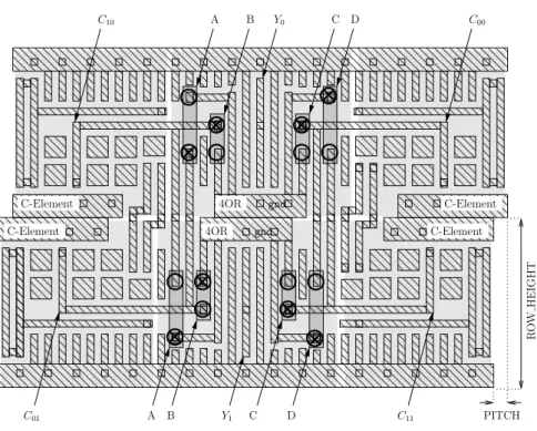
11 11 11 11 11 11 11 11 11 11 11 11 11 11 1 1 1 1 1 1 1 1 1 1 1 1 1 1 1 1 1 1 11 11 11 11 11 11 11 11 11 1111111 1111111 11111111 11111111 11111111 11111111 111111111111111111111111111111111 111111111111111111111111111111111 111111111111111111111111111111111 111 111111 111 111 111 11 11 11 11 11 11 11 11 1 1 1 11 11 11 1 1 1 11 11 11 11 11 11 1 1 1 1 1 1 1 1 1 1 1 1 1 1 1 1 1 1 1 1 1 1 1 11 11 11 11 11 11 111 111 111 111 11 11 11 11 11 11 11 11 11 11 11 11 11 1 1 1 1 1 11 11 11 11 11 11 1111111111 1111111111 11 11 1 1 1 1 1 1 1 1 1 1 111111111 111111111 11 11 1 11 11 11 11 11 11 11 1 1 1 1 1 1 1 11 11 11 11 11 11 11 11 11 11 11 111 111 11 11 11111111111 11111111111 1 1 1111 1111 1 1 1 1 1 1 1 1 1 1 1 11 11 11 11 11 11 11 11 11 11 11 11 11 11 11 11 11 11 11 11 1 1 1 1 1 1 11 11 11 11 11 11 11 1 1 1 1 1 1 1 1 1 1 1 1 1 1 1 11 1 1 1 1 1 1 1 1 11 11 111 1 1 1 1 11 11 11 11 11 11 11 11 1111111111 1111111111 11 11 1 1 1 1 1 1 1 1 1 1 1 1 1 1 11 11 1 1 1 1 1 1 11 11 11 11 11 11 11 11 11 11 11 11 1 1 1 1 1 1 1 1 1 11 11 11 1 1 1 1 1 1 11 11 11 1111111 1111111 1111111 11111111 11111111 11111111 11111111 11111111 11111111 11 1 1 1 1 1 1 1 111 111 111 111 111 111 111 111 111 11 11 11 11 11 11 11 11 11 11 11 11 11 11 11 11 11 11 11 11 11 11 11 11 11 11 11 11 11 11 11 1 1 11 11 11 11 11 11 11 11 11 1 1 1 1 1 1 1 1 1 11 11 11 11 11 1 1 1 1 1 1 1 1 1 11 11 11 11 11 11 11 1 1 1 1 1 1 11 11 11 11 11 11 1111111111 11 11 11 1 1 1 1 1 1 1 1 1 1 111111111 11 111 11 11 11 11 11 11 11 1 1 1 1 1 1 1 1 1 11 11 11 11 11 11 11 11 1 1 1 111 11 11 11111111111 111111111111 1111 1 1 1 1 1 1 1 1 1 1 1 1 1 1 1 11 11 11 11 11 11 11 11 11 11 11 11 11 11 1 1 1 1 11 1 1 1111 11 11 1 1 1 1 1 1 1 1 11 11 11 11 11 1 1 1 11 1 1 1 1 1 1 1 1 11 11 11 1 1 1 1 1 1 11 11 11 11 11 11 11 11 1111111111 1111111111 1 1 1 1 1 1 1 1 11 11 11 11 11 11 1 1 1 111111111111111111111111111111111 111111111111111111111111111111111 C-Element C-Element 4OR 4OR PITCH R O W H E IG H T C11 D Y1 C A B C01 C10 A B Y0 C D C00 C-Element C-Element gnd gnd
Figure 10: Layout of an unfinished SecLib gate: vias can be added at positions spotted by circles. Table 2: Connectivity within a two-input SecLib template gate to specialize it to a AND.
Input\ 4OR 4OR driving Y0 4OR driving Y1
A gnd or C01 gnd or C10
B gnd or C10 gnd or C01
C gnd or C00 gnd or C11
D gnd or C11 gnd or C00
A
Generation of the Layout of Two-Input SecLib Gates from
one Template
This section explains how to generate multiple two-input gates from one single GDS2 template. The structure given in Fig. 1 involves a 3OR gate. For symmetry reasons, this 3OR gate is actually one 4OR with one input shorted to the ground. We provide in Fig. 10 with the layout (only metal-2 is shown) of an unbalanced (XOR and XNOR are excluded) two-input gate template.
The four inputs A, B, C & D of the 4OR can be connected either to the ground or to one C-Element gate output. The connection points are indicated by a circle ( ) in Fig. 10. One via is instantiated to choose the adequate connection; it is represented by a cross into the circle (N) in Fig. 10. Table 2 summarizes the connection possibilities; the vias are indicated by underlining the selected input for each input of the two 4OR gates driving the differential output (Y0, Y1).
B
Generation of the Behavioral Description of Two-Input
Se-cLib Gates from one Template
The VHDL behavioral description of n-input QDI gates, upon which SecLib gates are built, is listed below. It enables fast functional simulations of SecLib netlists.
1 −− @ f i l e q d i . vhd
−− @ b r i e f The b e h a v i o r a l s p e c i f i c a t i o n o f t h e q u a s i −d e l a y i n s e n s i t i v e ( aka QDI) −− p r i m i t i v e s used i n S e c L i b ( S e c u r e d L i b r a r y ) l o g i c .
l i b r a r y i e e e ;
6 use i e e e . s t d l o g i c 1 1 6 4 . a l l ;
−− M u l t i p l e i n p u t / s i n g l e o u t p u t 1−of −2 f o u r −p h a s e QDI g a t e b e h a v i o r a l model :
e n t i t y q d i i s generic 11 ( t t : s t d u l o g i c v e c t o r −− Truth t a b l e ) ; port (
16 −− A( F a l s e , True ) , B( F a l s e , True ) , C( F a l s e , True ) [ i f a ’ l e n g t h = 6 ] .
a : in s t d u l o g i c v e c t o r ;
y : out s t d u l o g i c v e c t o r ) ;
begin
21 a s s e r t a ’ l e n g t h mod 2 = 0 and y ’ l e n g t h = 2
report ”QDI g a t e p o r t s a r e not dual− r a i l ”
s e v e r i t y f a i l u r e ;
a s s e r t t t ’ l e n g t h = 2 ∗ ∗ ( a ’ l e n g t h / 2 )
report ”QDI g a t e t r u t h t a b l e has a bad d i m e n s i o n ”
26 s e v e r i t y f a i l u r e ; end e n t i t y q d i ; arch it e ct u re beh of q d i i s s i g n a l c : s t d u l o g i c v e c t o r ( 0 to 2 ∗ ∗ ( a ’ l e n g t h / 2 ) − 1 ) ; −− ‘ ‘ a ’ ’ decoded 31 −− E v a l u a t e s w h e t h e r one ’ 1 ’ o f t h e t r u t h t a b l e i s h i t . Models an OR g a t e : function e v a l ( s i g n a l c : in s t d u l o g i c v e c t o r ) return s t d u l o g i c v e c t o r i s v a r i a b l e r e s u l t : s t d u l o g i c v e c t o r ( 0 to 1 ) := ” 00 ” ; begin 36 f o r I in c ’ range loop
i f ( not t t ( I ) and c ( I ) ) = ’ 1 ’ then r e s u l t ( 0 ) := ’ 1 ’ ; end i f ;
i f ( t t ( I ) and c ( I ) ) = ’ 1 ’ then r e s u l t ( 1 ) := ’ 1 ’ ; end i f ;
end loop; return r e s u l t ; 41 end function e v a l ; begin −− Example on 3 b i t s : −− +−−−−−−−−−−−−−−+−−−−−−−−−−+ −− | | A B C | 46 −− | 0 1 2 | 01 01 01 | <= ”01” means ”True , F a l s e ” −− +−−−−−−−−−−−−−−+−−−−−−−−−−+ −− | c ( ”0 0 0” ) | YN YN YN | <= B i t s t o t e s t (Y=Yes , N=No) a g a i n s t 0 or 1 −− | c ( ”0 0 1” ) | NY YN YN | −− | c ( ”0 1 0” ) | YN NY YN | 51 −− | c ( ”0 1 1” ) | NY NY YN | −− | c ( ”1 0 0” ) | YN YN NY | −− | c ( ”1 0 1” ) | NY YN NY | −− | c ( ”1 1 0” ) | YN NY NY | −− | c ( ”1 1 1” ) | NY NY NY | 56 −− +−−−−−−−−−−−−−−+−−−−−−−−−−+
G DECODE: f o r C I in c ’ range generate
−− T e s t i n g c o n c o m i t a n t ‘ ‘ a l l 0 ’ ’ and ‘ ‘ a l l 1 ’ ’ b i t s :
P SEQUENTIAL C I : process ( a ) −− Models a C−Element w i t h a ’ l e n g t h /2 i n p u t s
−− The t y p e ‘ ‘ b o o l e a n v e c t o r ’ ’ d o e s n o t e x i s t i n VHDL, u n f o r t u n a t e l y :
61 v a r i a b l e rdv : b i t v e c t o r ( 0 to 1 ) ;
−− T e s t s w h e t h e r or n o t t h e b i t a t p o s i t i o n ‘ ‘ pos ’ ’ o f t h e (32− b i t )
−− i n t e g e r i s s e t .
function i s s e t ( a : i n t e g e r ; pos : n a t u r a l ) return b o o l e a n i s
begin 66 a s s e r t pos < 32 −− P o r t a b i l i t y n o t i c e report ” I n t e g e r s a r e o f t e n r e p r e s e n t e d a s 32− b i t s t r i n g s ” s e v e r i t y warning ; i f ( a /2∗∗ pos mod 2 ) = 0 then return f a l s e ; 71 e l s e return t r u e ; end i f; end function i s s e t ;
function i s s e t ( a : i n t e g e r ; pos : n a t u r a l ) return i n t e g e r i s
begin 76 i f i s s e t ( a , pos ) then return 1 ; e l s e return 0 ; end i f; end function i s s e t ; 81 begin rdv := ” 11 ” ; −− By d e f a u l t , a d o u b l e RdV . . . now c a n c e l l i n g t h e bad c h o i c e s
f o r ABC in 0 to a ’ l e n g t h / 2 −1 loop −− n i t e r a t i o n s f o r n−i n p u t g a t e s
i f A( 2 ∗ ABC + i s s e t ( C I , ABC ) ) = ’ 1 ’ −− The b i t i s s e t
then rdv ( 0 ) := ’ 0 ’ ; −− No rendez −vous t o ‘ ‘ 0 ’ ’
86 e l s e rdv ( 1 ) := ’ 0 ’ ; −− No rendez −vous t o ‘ ‘ 1 ’ ’
end i f;
end loop; −− On A, B, C, e t c . d u a l −r a i l s i g n a l s c o n c a t e n a t e d i n ‘ ‘ a ’ ’
a s s e r t not( ( rdv ( 0 ) and rdv ( 1 ) )= ’ 1 ’ )
report ”One C−Element r e p o r t e d a r e n d e z −vous t o both ‘ ‘ 0 ’ ’ and ‘ ‘ 1 ’ ’ ”
91 s e v e r i t y f a i l u r e ;
−− Updating ‘ ‘ c ’ ’ o n l y i f t h e r e were a c t u a l l y a rendez−vous :
i f rdv ( 0 ) = ’ 1 ’ then c ( C I ) <= ’ 0 ’ ; end i f ;
i f rdv ( 1 ) = ’ 1 ’ then c ( C I ) <= ’ 1 ’ ; end i f ;
end process P SEQUENTIAL C I ;
96 end generate G DECODE;
P OUTPUT: y <= e v a l ( c ) ;
end arch it e ct u re beh ;
101 l i b r a r y i e e e ; use i e e e . s t d l o g i c 1 1 6 4 . a l l ; use work . a l l ; 106 −− Two−i n p u t QDI g a t e e n t i t y q d i 2 i s generic ( t t : s t d u l o g i c v e c t o r −− Truth t a b l e 111 ) ; port (
−− a ( F a l s e , True ) , b ( F a l s e , True ) => y ( F a l s e , True )
A0 , A1 , B0 , B1 : in s t d u l o g i c ;
116 Z0 , Z1 : out s t d u l o g i c
) ;
arch it e ct u re a d a p t o r of q d i 2 i s
121 s i g n a l i n p u t s : s t d u l o g i c v e c t o r ( 0 to 3 ) ; −− A F a l s e A True | | B F a l s e B True
s i g n a l o u t p u t s : s t d u l o g i c v e c t o r ( 0 to 1 ) ; −− Z F a l s e Z True
begin
P INPUTS : i n p u t s <= A0 & A1 & B0 & B1 ; I QDI : entity q d i ( beh )
126 generic map( t t => t t )
port map( a => i n p u t s , y => o u t p u t s ) ;
P OUTPUTS Y0 : Z0 <= o u t p u t s ( 0 ) ; P OUTPUTS Y1 : Z1 <= o u t p u t s ( 1 ) ;
end arch it e ct u re a d a p t o r ;
Finally, the behavioral description of the SecLib AND gate is given below:
l i b r a r y i e e e ;
use i e e e . s t d l o g i c 1 1 6 4 . a l l ;
use work . a l l ; −− For t h e v i s i b i l i t y o f t h e p r e v i o u s l y d e s c r i b e d e n t i t y ” q d i 2 ”
5 e n t i t y SAN2 X1 i s port ( A0 , A1 , B0 , B1 : in s t d u l o g i c ; Z0 , Z1 : out s t d u l o g i c 10 ) ; end e n t i t y SAN2 X1 ; arch it e ct u re t e m p l a t e of SAN2 X1 i s begin 15 I QDI2 : entity q d i 2 ( a d a p t o r ) generic map( t t => ” 0001 ” ) port map( A0 => A0 , A1 => A1 , B0 => B0 , B1 => B1 , Z0 => Z0 , Z1 => Z1 ) ; end arch it e ct u re t e m p l a t e ;