Institut National de la Recherche Scientifique Énergie Matériaux Télécommunications
A CMOS COMPATIBLE
FERROELECTRIC TUNNEL JUNCTION MEMORY DEVICE
parFabian Ambriz Vargas
Thèse présentée pour l’obtention du grade de Philosophiae Doctor (Ph.D.)
en Sciences de l’énergie et des matériaux
Jury d’évaluation
Président du jury Professeur Shuhui Sun, INRS - EMT, Canada Examinatrice externe Professeure Clara Santato,
École Polytechnique de Montréal, Canada Examinateur externe Professeur Ashish Garg,
Indian Institute of Technology Kanpur, India Co-directeur de recherche Professeur Marc André Gauthier,
INRS – EMT, Canada
Directeur de recherche Professeur Andreas Peter Ruediger, INRS – EMT, Canada
Acknowledgements
In first instance, I would like to acknowledge Professor Andreas Ruediger and Professor Marc André Gauthier for gave me the opportunity to come to Canada and develop my Ph.D. project. Also, I acknowledge the time, that both of you invested in reviewing, discussing and guiding me during the last few years. Through the development of this project, I felt working at the frontiers of the semiconductor memory field; therefore, I would like to acknowledge both of you for empowering the students. Thanks for make us believe that our projects can create an impact on the scientific community.
I acknowledge the examiners, Professor Shuhui Sun, Professor Clara Santato and Professor Ashish Garg, for accepting to review and evaluate this work.
I want to acknowledge all the members (students and postdoctoral fellows) of the
Nanophotonics and Gauthier groups. Specially, Julien Plathier and Thameur Hajlaoui for help me
with the redaction and revision of the french section. Also, I would like to acknowledge professor Reji Thomas for guided me during the first half of my Ph.D. project as well as offered me his valuable friendship.
The film deposition process was assisted with the help of the employers of Plasmionique
inc. Therefore, I acknowledge Dr. Sarkissian and Dr. Rafik Nouar for gave me their advisory.
Also, I acknowledge Dr. Andranik Sarkissian for reviewed my manuscripts, and for invited me to several conferences related to physical vapor deposition techniques.
I want to acknowledge both agencies Fonds de recherche du Québec - Nature et
Technologies (FRQNT-Canada) and Consejo Nacional de Ciencia y Tecnología
(CONACyT-Mexico) for provided me the financial support.
Finally, I acknowledge my family (Mother, father, sisters and brother) for gave their support, love and patience. I want to acknowledge the driving force of my life; my beloved wife (Josefina Crespo Villegas), the righteousness person I have ever met and also, I acknowledge my daughter (Nina Pastelita). Both wife and daughter are my spiritual masters in this game called life.
With special dedication to my sweet angels; Maria Britany, Gatito Caballerito Muffin and Luna Margarita.
Abstract
The semiconductor electronic industry has been searching for a universal memory that combines fast write/read access with non-volatility and excellent scalability. To realize such an ambitious task, the following is required: Non-volatility like FLASH memory, scalability to high density like dynamic random access memory (DRAM) and FLASH, high speed like static random access memory (SRAM) and high endurance like DRAM and SRAM. To date, none of the commercially available solutions responds to all of those requirements.
Among the different emerging semiconductor memories, ferroelectric tunnel junctions (FTJs) are the most promising candidates to become a universal memory. An FTJ device is a resistance-based memory that combines good scalability (simple cell size: 1 capacitor-1transistor) with low operating energy, non-volatility, high operation speed (write time, <10 ns) and high endurance (>106 cycles).
In 2009, the fabrication of the first FTJ memory device based on a perovskite tunnel barrier (BaTiO3) was reported. However, the integration of perovskite materials into the conventional
silicon technology remains challenging due to their lack of compatibility with the complementary metal oxide semiconductor process (CMOS). In this context, the present thesis reports on; the fabrication and evaluation of the first FTJ memory device based on CMOS-compatible materials and deposition processes.
The deposition of ferroelectric ultrathin films with only a few unit cells thickness is a crucial challenge in the development of FTJ memory devices. As such, the effect of the layer thickness on the ferroelectric properties of BaTiO3 was studied first. Chapter four presents a
detailed study of the growth mechanism of BaTiO3 on Nb:SrTiO3 substrates for on-axis
RF-magnetron sputtering. The optimization of the deposition parameters to prevent substrate re-sputtering in order to allow the transfer of the correct stoichiometry from the target to the Nb:SrTiO3 substrate surface is reported.
In most cases, literature reports the use of atomic layer deposition (ALD) and pulsed laser deposition (PLD) to grow ultrathin BaTiO3 films. In the case of ALD, the deposition process of
temperature of 280oC while the second step consists in the annealing of the as-deposited film (at a relative high temperatures 900oC) to allow its crystallization. In the case of PLD, it achieves the deposition of crystalline BaTiO3 in a single step, at a substrate temperature of 900oC.
Although PLD is well suited for maintaining the stoichiometry of crystalline BaTiO3, this process
is not scalable. On the other hand, sputtering is a widely used deposition technique for large-scale production. Thus, in this thesis, crystalline BaTiO3 was deposited in a single step at a
relative low substrate temperature (650oC). However, this substrate temperature is still too high
to be compatible with the semiconductor industry process. Therefore, it was necessary to search for new material candidates.
The recent discovery of ferroelectricity in Si-doped HfO2 and Hf0.5Zr0.5O2 films has
renewed the interest for realizing ferroelectric tunnel junction devices, since ZrO2 and HfO2 are
familiar to the semiconductor industry. Thus, in chapter five, Hf0.5Zr0.5O2 was evaluated as a
possible candidate for an FTJ memory device. The fabrication of two types of FTJ memories (nominally symmetric-FTJ and asymmetric-FTJ) made of CMOS compatible materials (Hf0.5Zr0.5O2 as ferroelectric tunnel barrier and TiN as an electrode) is reported. In both types of
FTJ memories, the electronic charge transport across the semiconductor/ferroelectric interfaces was studied by current-voltage curves. X-ray photoelectron and UV-VIS spectroscopies established a quantitative model for the band diagram. The combination of experimental data obtained from conductive-atomic force microscopy with theoretical models described by Simmons (nominally symmetric-FTJs) and Brinkman (asymmetric-FTJs) attested to the presence of the “tunneling electroresistance effect (TER effect)” in both FTJ memory devices. Furthermore, an evaluation of our FTJ memory device was performed, demonstrating excellent semiconductor memory properties (good endurance, good data-retention, large TER ratio at low voltages combined with a reproducible deposition process).
KEYWORDS: Ferroelectric tunnel junction memory, Ferroelectrics; Thin films
The following chapters are based on and contain word-by-word excerpts of references
[1-6]. My contribution to this work was critical regarding the conception of the experiments for
both thin film deposition and characterization, the execution of the experiments, the data analysis and the participation in the scientific discussion as well as the redaction of the manuscripts.
Résume
L’industrie des semi-conducteurs est à la recherche d’une mémoire universelle combinant la vitesse de lecture et d’écriture des mémoires statiques (SRAM – Static Random Access Memory) ; la non-volatilité des mémoires flash ; et la haute densité d’informations ainsi que l’endurance des mémoires statiques (DRAM – Dynamic Random Access Memory). À ce jour, aucune solution disponible commercialement remplis ces critères ambitieux.
Parmi les différentes solutions émergentes, les mémoires ferroélectriques à jonction tunnel (FTJ – Ferroelectric Tunnel Junction) sont les candidates les plus prometteuses au titre de mémoire universelle. La FTJ est une mémoire utilisant le changement de sa résistance électrique pour stocker l’information qui allie une grande vitesse d’opération (temps d’écriture : ~10 ns) avec une faible volatilité, une haute densité d’informations (1 bit est composé uniquement d’une capacité et d’un transistor) et une haute endurance (106 cycles) ; le tout ne nécessitant qu’une faible quantité
d’énergie.
En 2009, la fabrication de la première mémoire ferroélectrique à jonction tunnel, basée sur une barrière tunnel composée d’un matériau de la famille des pérovskites, le titanate de baryum, a été annoncée. Cependant, intégrer les pérovskites dans les procédés conventionnels de la technologie du silicium reste un défi causé par la faible compatibilité des méthodes de croissance des pérovskites avec les procédés de fabrication des composants électroniques (CMOS – Complementary Metal-Oxide Semiconductor). Dans ce contexte, cette thèse présente la première fabrication et caractérisation d’un dispositif mémoire FTJ utilisant des matériaux compatibles avec le procédé CMOS.
La déposition de couches ferroélectrique ultraminces est un défi majeur dans le développement des dispositifs mémoire FTJ. Ainsi, l’effet de l’épaisseur de la couche sur les propriétés du titanate de baryum, l’un des matériaux ferroélectriques les mieux connus, a été étudié en détail en premier lieu. Cette étude, présentée dans le chapitre 4, explore le mécanisme de croissance du titanate de baryum (BaTiO3) sur un substrat de titanate de strontium dopé avec du
Le titanate de baryum comme barrière ferroélectrique ultramince a déjà été utilisé dans d’autres dispositifs mémoire FTJ. Dans la plupart des cas, les méthodes utilisée pour la croissance du titanate de baryum sont le dépôt atomique de couches (ALD – Atomic layer deposition) et l’ablation par laser pulsée (PLD – Pulsed laser deposition). Dans le cas de l’ALD, le dépôt s’effectue en deux étapes. D’abord, une couche amorphe de titanate de baryum est déposée sur le substrat chauffé à 280°C. Ensuite, un recuit de la couche permet la cristallisation. Dans le cas de la PLD, la déposition du titanate de baryum cristallin est effectuée en une seule étape en chauffant le substrat à 900°C. Bien que la PLD permette d’obtenir titanate de baryum cristallin avec la même stœchiométrie que la cible de déposition, ce procédé ne peut pas être utilisé à l’échelle industrielle. Cependant, le dépôt par pulvérisation cathodique est une méthode répandue pour la production à grande échelle. Par conséquent, dans cette thèse le titanate de baryum cristallin est déposé en une étape avec un substrat à une température relativement faible (650°C) en utilisant le dépôt par pulvérisation cathodique magnétron. Néanmoins, cette température reste trop élevée pour les procédés de l’industrie des semi-conducteurs. Il a donc été nécessaire de chercher d’autres matériaux ferroélectrique et compatible avec procédés industriels.
La découverte récente de la ferroélectricité dans les couches minces d’oxyde d’hafnium (HfO2) et d’oxyde d’hafnium-zirconium (Hf0.5Zr0.5O2) a renouvelé l’intérêt dans la réalisation de
dispositifs mémoire FTJ puisque cette famille de matériaux est déjà utilisée par l’industrie du silicium. Ainsi, l’oxyde d’hafnium-zirconium est étudié dans le chapitre 5 comme candidat possible pour les dispositifs mémoire FTJ. Deux types de dispositifs (le symétrique et le FTJ-asymétrique), compatibles avec la technologie CMOS ont été fabriqués en utilisant l’oxyde d’hafnium-zirconium comme barrière tunnel ferroélectrique et le nitrure de titane (TiN) comme électrodes. Pour chaque dispositif, le transport des charges à travers les interfaces ferroélectrique/semi-conducteur sont étudiées en utilisant la spectrométrie de photoélectrons induits par rayons X (XPS – X-ray photoelectron spectrometry) et spectroscopie UV-Visible. La combinaison des données expérimentales, obtenue par microscopie à force atomique en mode conduction de courant (C-AFM – Conductive-Atomic Force Microscopy), et des modèles théoriques décrits par Simmons (FTJ-symétrique) et par Brinkman (FTJ-asymétrique) démontre la présence d’électrorésistance à effet tunnel (TER – Tunneling ElectroResistance) dans les deux types de dispositifs mémoire FTJ. De plus, la caractérisation de nos dispositifs démontre
d’excellentes propriétés de mémoire semi-conductrice (bonne endurance et rétention de l’information, grand ratio TER à faibles tensions et un procédé de fabrication reproductible).
MOTS-CLÉS : Mémoires ferroélectriques à jonction tunnel; matériaux ferroélectriques; couches minces
Les prochains chapitres sont basés et contiennent des extraits des références [1-6]. J’ai apporté une contribution majeure à ces travaux en ce qui concerne la conception et la réalisation des expériences de synthèse et de caractérisation, l’analyse de données, la discussion des résultats, et la rédaction des manuscrits.
Publications, presentations and awards
PUBLISHED REFEREED ARTICLES[1] G. Kolhatkar, F. Ambriz-Vargas, B. Huber, R. Thomas and A. Ruediger; Thermionic Emission Based Resistive Memory with Ultra-Thin Ferroelectric BiFe(1-x)CrxO3 Films Deposited
by Mineralizer-Free Microwave-Assisted Hydrothermal Synthesis; ACS-Crystal Growth &
Design; 10.1021/acs.cgd.7b01745 (2018).
[2] F. Ambriz-Vargas, G. Kolhatkar, M. Broyer, A. Hadj-Youssef, R. Nouar, A. Sarkissian, R. Thomas, C. Gomez-Yáñez, M. A. Gauthier and A. Ruediger; A Complementary Metal Oxide Semiconductor Process-Compatible Ferroelectric Tunnel Junction; ACS Applied Materials &
Interfaces, 9 (15), 13262–13268 (2017).
[3] F. Ambriz-Vargas, G. Kolhatkar, R. Thomas, R. Nouar, A. Sarkissian, C. Gomez-Yáñez, M. A. Gauthier, and A. Ruediger; Tunneling Electroresistance Effect in a Pt/Hf0.5Zr0.5O2/Pt
Structure; Applied Physics Letters, 110, 093106 (2017).
[4] F. Ambriz-Vargas, R. Nouar, G. Kolhatkar, A. Sarkissian, R. Thomas, C. Gomez-Yáñez, M. A. Gauthier, A. Ruediger; RF-magnetron Sputtering Deposition of Ultra-thin Hf0.5Zr0.5O2 Films
for Non-volatile Memory Applications; Materials today: Proceedings; 4 (7), 7000-7010 (2017).
[5] F. Ambriz-Vargas, R. Zamorano-Ulloa, A. Romero-Serrano, J. Ortiz-Landeros, J. Crespo-Villegas, D. Ramírez-Rosales and C. Gómez-Yáñez; Point-defect Chemistry on the Polarization Behavior of Niobium Doped Bismuth Titanate; Journal of the Mexican Chemical Society; 61, 317-325 (2017).
[6] G. Kolhatkar, F. Ambriz-Vargas, R. Thomas and A. Ruediger; Microwave-assisted Hydrothermal Synthesis of BiFexCr1-xO3 Ferroelectric Thin Films; Crystal Growth & Design, 17
(11), 5697-5703 (2017).
[7] F. Ambriz-Vargas, I. Velasco-Davalos, R. Thomas and Andreas Ruediger; Nucleation and Growth of Ultrathin BaTiO3 Films on Single Terminated Nb:SrTiO3 (100) Substrates for
Ferroelectric Tunnel Junction; Journal of Vacuum Science & Technology B, 34, 02M101 (2016).
[8] I. Velasco-Davalos, F. Ambriz-Vargas, C. Gómez-Yáñez, R. Thomas and A. Ruediger; Polarization Reversal in BaTiO3 Nanostructures Synthesized by Microwave-assisted
Hydrothermal Method; Journal of Alloys and Compounds, 667, 268-274 (2016).
[9] I. Velasco-Davalos, F. Ambriz-Vargas, G. Kolhatkar, R. Thomas and A. Ruediger; Synthesis of BiFeO3 Thin Films on Single-terminated Nb:SrTiO3 (111) Substrates by Intermittent
Microwave Assisted Hydrothermal Method; American Institute of Physics, Advances, 6 (6), 10.1063 (2016).
[10] Y. Ayadi, L. Rahhal, B. Vilquin, C. Chevalier, F. Ambriz-Vargas, S. Ecoffey, A. Ruediger, A. Sarkissian, S. Monfray, J. Cloarec, D. Drouin and A. Souifi; Novel Concept of Gas Sensitivity Characterization of Materials Suited for Implementation in FET-Based Gas Sensors; Nanoscale
Research Letters, 11(481), 1-7 (2016).
[11] F. Ambriz-Vargas, R. Nouar, Z. Said Bacara, B. Higuera, R. Porter, A. Sarkissian, R. Thomas and A. Ruediger; On-axis radio Frequency Magnetron Sputtering of Stoichiometric BaTiO3 Target: Localized Re-sputtering and Substrate Etching During Thin Film Growth; Thin Solid Films, 596, 77-82 (2015).
[12] I. Velasco-Davalos, F. Ambriz-Vargas, R. Thomas, A. Ruediger; Surface Preparation of (110) Oriented Pure and Nb Doped SrTiO3 Single Crystal Substrates by Microwave Assisted
Hydrothermal Method; Surface & Coatings Technology, 283, 108-114 (2015).
PUBLISHED BOOK CHAPTERS
[13] F. Ambriz-Vargas, R. Thomas and A. Ruediger; Ferroelectric (Hf,Zr)O2 Thin Films for High
Density Non-volatile Memories?; Frontiers in Materials Processing, Applications, Research and
Technology: FiMPART 2015; ISBN 978-981-10-4819-7 (2018).
PATENTS
Title: Ferroelectric tunnel junction and a method of fabrication thereof.Patent location: United States of America and Canada
Patent reference number: US 2018 773/14448.113
Inventors: Fabian Ambriz-Vargas, Gitanjali Kolhatkar, Thomas Reji, Rafik Nouar, Azza Hadj Youssef, Andranik Sarkissian, Marc A. Gauthier, Andreas Ruediger
CONFERENCE CONTRIBUTIONS
[1] Fabian Ambriz-Vargas, Gitanjali Kolhatkar, Rafik Nouar, Andranik Sarkissian, Marc A. Gauthier and Andreas Ruediger; Fabrication of a CMOS Compatible, Ferroelectric Tunnel
Junction Memory; International Conference on Metallurgical Coatings and Thin Films;
California-United stated of America (2018, oral presentation).
[2] Fabian Ambriz-Vargas, Gitanjali Kolhatkar, Thomas Reji, Rafik Nouar, Andranik Sarkissian, Marc A. Gauthier and Andreas Ruediger; A CMOS Compatible, Ferroelectric Tunnel Junction
Memory; 23rd International Symposium on Plasma Chemistry; Montreal-Canada (2017, poster
presentation).
Memory; Functional Coating and Surface Engineering symposium; Montreal-Canada (2017,
poster presentation).
[4] Fabian Ambriz-Vargas, Gitanjali Kolhatkar, Thomas Reji, Rafik Nouar, Andranik Sarkissian, Marc A. Gauthier and Andreas Ruediger; A CMOS Compatible, Ferroelectric Tunnel Junction
Memory; Surface Canada 2017; Montreal-Canada (2017, poster presentation).
[5] Fabian Ambriz-Vargas, Gitanjali Kolhatkar, Thomas Reji, Rafik Nouar, Andranik Sarkissian, Marc A. Gauthier and Andreas Ruediger; A CMOS Compatible, Ferroelectric Tunnel Junction
Memory; Colloque Plasma-Québec 2017; Montreal-Canada (2017, poster presentations).
[6] Fabian Ambriz-Vargas, Marc A. Gauthier, Rafik Nouar, Andranik Sarkissian and Andreas Ruediger. Resistive Switching in Pt/Hf0.5Zr0.5O2/Pt and TiN/ Hf0.5Zr0.5O2/TiN Structures. 14th
International Conference on Nanosciences & Nanotechnologies; Thessaloniki-Greece (2016,
oral presentation).
[7] Fabian Ambriz-Vargas, Gitanjali Kolhatkar, Thomas Reji, Rafik Nouar, Andranik Sarkissian, Marc A. Gauthier and Andreas Ruediger; RF Magnetron Sputtering of Hf0.5Zr0.5O2 Thin Films;
Colloque Plasma-Québec 2016; Montreal-Canada (2016, poster presentation).
[8] Fabian Ambriz-Vargas, Thomas Reji, Rafik Nouar, Andranik Sarkissian, Marc A. Gauthier and Andreas Ruediger. RF Magnetron Deposition of Ultrathin BaTiO3 Films; 17th Canadian
Semiconductor Science and Technology Conference; Sherbrook-Canada (2015, oral presentation).
[9] Fabian Ambriz-Vargas, Gitanjali Kolhatkar, Thomas Reji, Rafik Nouar, Andranik Sarkissian, Marc A. Gauthier and Andreas Ruediger; Ferroelectric Hf0.5Zr0.5O2 Ultrathin Films; Colloque
Plasma-Québec 2015; Montreal-Canada (2015, poster presentation).
AWARDS
[1] – Merit doctoral research scholarship program for foreign students (PBEEE) du Fonds de
recherche du Québec Nature et technologies (FRQNT) from January 2015 to May 2018.
[2] – Ph.D. scholarship for international students provided by the National Council of Science
Contents
Acknowledgements ... i
Abstract ... iii
Publications, presentations and awards ... ix
Contents ... xiii
CHAPTER 1 Introduction ... 1
1.1 Research objectives ... 4
1.2 Specific objectives ... 4
CHAPTER 2 State of the art... 5
2.1 Semiconductor memories ... 5
2.2 Emerging semiconductor memories ... 7
2.3 Thin film growth process ... 12
2.4 Polarization properties ... 15
2.5 Solid solution hafnium zirconium oxide ... 18
2.6 Electronic charge transport at the semiconductor interface ... 22
2.7 Charge transport in metal-insulator-metal devices ... 24
CHAPTER 3 Characterization tools ... 29
3.1 Deposition techniques ... 29
3.2 Structural characterization tools ... 32
3.3 Chemical characterization tools ... 35
3.4 Microstructural characterization tools ... 37
CHAPTER 4 Ferroelectric tunnel junction based on BaTiO3 ... 39
4.2 Experimental section ... 40
4.3 Localized re-sputtering and substrate etching during thin film growth ... 43
4.3.1 Stoichiometry of as-deposited BaTiO3 films ... 46
4.3.2 Summary ... 48
4.4. Fabrication of a Nb:SrTiO3/BaTiO3/Pt-tip heterostructure... 49
4.4.1 Growth mechanism of a BaTiO3 on a Nb:SrTiO3 substrate ... 50
4.4.2 Ferroelectricity of BaTiO3 in ultrathin film form ... 52
4.4.3 Summary ... 53
CHAPTER 5 Ferroelectric tunnel junction based on Hf0.5Zr0.5O2 ... 55
5.1 Hafnium-Zirconium oxide film... 55
5.2 Experimental section ... 56
5.3 Optimization of the Hf0.5Zr0.5O2 deposition parameters ... 58
5.3.1 Microstructural characterization... 58
5.3.2 Chemical characterization ... 58
5.3.3 Ferroelectricity as a function of deposition temperature ... 59
5.3.4 Ferroelectricity as a function of film thickness... 61
5.3.5 Summary ... 63
5.4 Nominally symmetric FTJ memory device (Pt/Hf0.5Zr0.5O2/Pt) ... 64
5.4.1 Fabrication of the nominally symmetric FTJ memory device ... 64
5.4.3 Electronic properties of the nominally symmetric FTJ memory device ... 66
5.4.4 Tunneling electroresistance effect in the nominally symmetric FTJ memory device .. 69
5.4.5 Summary ... 71
5.5 Asymmetric FTJ memory device (TiN/Hf0.5Zr0.5O2/Pt) ... 72
5.5.1. Fabrication of the asymmetric FTJ memory device ... 72
5.5.2 Ferroelectric characterization of the asymmetric FTJ memory device ... 74
5.5.3 Electronic properties of the asymmetric FTJ memory device ... 75
5.5.4 Tunneling electroresistance effect on the asymmetric FTJ memory device ... 78
5.5.5 Evaluation of the asymmetric FTJ memory device ... 80
5.5.6 Summary ... 81
Summary and outlook ... 83
Appendix A (Thickness measurements and XPS calibration) ... 87
Appendix B (Platinum structural properties) ... 89
Appendix C (Ferroelectric retention measurements) ... 90
Appendix D (Band alignment determination)... 91
Appendix E (Simmons and Brinkman models) ... 94
References ... 97
Abbreviations ... 107
Chapter 1 Introduction
Recent technology improvements in micro- and nano- fabrication techniques have brought a new generation of electronic devices to the market, such as computers, cellphones, cameras, tablets, etc.7-9 In addition to being slimmer and lighter, these devices possess more storage capacity, they are faster, and also have an improved camera resolution. As predicted by “Moore’s law”, customers have been experiencing the birth of new generations of electronic devices every couple of years, during the last four decades. This trend has led the customers to continually expect more powerful and cheaper devices. However, that may not be the case if the electronic industry continues working with the current semiconductor memory technology.10
The key issue of current electronic devices is that they rely on the performance of a set of different semiconductor memories that have already reached their physical limits. In general, the processor within the central processing unit (CPU) of any personal computer is serviced by a series of memory technologies (Memory hierarchy in Table 1). The closest memory to the CPU is called “Cache memory” and it is comprised of a static random access memory (SRAM),7 it is very fast
(write/erase time: 0.3 ns/ 0.3 ns) but it is relative large in cell size (six transistors with a minimum cell size of 140F2, where “F” is the minimum feature size). Given their physical properties, SRAMs are used to provide fast access to instructions and data to the processor.7 In the next level of the hierarchy appears the “Principal memory”, which is comprised of a dynamic random access memory (DRAM). Contrary to SRAM, it is more compact (one-transistor and one-capacitor, with a cell size of 6F2) but it is slower (write/erase time: 10ns/10ns).7 The physical properties of DRAM allow it to reach high densities on a memory chip. The “Principal memory” is used to store and to process temporary information from the “Secondary memory” (hard disk).7 In both cases, the
“Cache” and the “Principal” memories are volatile (stored information will not remain when the energy power supply is turned off). “Secondary memory (solid state hard drive)” is mostly a flash memory, it is an external memory with non-volatile nature (it holds the information when the power supply is turned off). In comparison to the “Primary and Cache memories” it is really slow (write/erase time: 1ms/10ms).7, 10
As can be seen, the dominant memory types in modern electronics are dynamic-RAM (DRAM), static-RAM (SRAM), and FLASH memories.8-9, 11-12 These three types of memories
store data as a charge state. For many decades these memory technologies have been successfully scaled down to achieve higher speeds and increased density of memory chips at lower cost. However, they have gradually approached their physical limits of scalability.8, 11, 13 Therefore, for further advance in information processing/storage technologies, it is necessary to develop a universal memory than can replace the above conventional memories. To accomplish with this goal the universal memory should combine the best features of the current memories. For instance, it should combine the non-volatile nature of FLASH with the high scalability of DRAM, high speed of SRAM and high endurance of DRAM and SRAM (Table 1).7, 12
Table 1. Memory hierarchy and memory properties. Data obtained from ref. [7]
MEMORY HIERARCHY MEMORY PROPERTIES Processor (CPU) Speed
(Write/erase time)
Scalability (Cell size)
Endurance
(Cycles) Energy efficiency Cache memory (0.3ns/0.3ns) HIGH (140FLOW 2)
HIGH
(1016) VOLATILE
Primary memory (10ns/10ns) HIGH (6FHIGH 2)
HIGH
(1016) VOLATILE
Secondary memory LOW
(1ms/10ms)
HIGH (10F2)
LOW
(105) NON-VOLATILE
Universal memory HIGH HIGH HIGH NON-VOLATILE
Nowadays, there are emerging semiconductor memories based on different physical approaches that could satisfy the positive points of DRAM, SRAM, and FLASH.7, 12 Among the different noticeable types of emerging memories, the strongest candidate to become a universal memory is the ferroelectric tunnel junction memory (FTJ).
An FTJ memory device is composed of two metal electrodes separated by a nanometer-thick ferroelectric layer (1-3 nm in nanometer-thickness).14-16 The physical concept of this memory is based
on the tunneling electroresistance effect, (TER effect). This process consists in the reversible modulation of the electrical resistance state by using an electric field.14-16 This modulation gives
place to the formation of two stable states (High resistance state, “HRS” and low resistance state, “LRS”), which can be codified as “1” and “0” in a binary code.14-16
The first experimental demonstration of the TER effect was reported in 2009 by M. Bibes (Nature Letters)17 and A. Gruverman (Nanoletters).9 In both cases, BaTiO3 was used as an ultrathin
ferroelectric layer. These results triggered an intense research on the study of the properties of the FTJs, where it was demonstrated that the physical concept of the FTJ memory can bring important advantages such as high fatigue resistance (endurance ~ 106 cycles),18-19 high speed (“ON/OFF”
states can be written with pulses down to 10 ns),20 high scalability,15 and simple architecture.14 Despite the excellent memory properties of FTJ devices, their introduction into the semiconductor market has been restricted because integrating FTJs based on ferroelectric perovskite ultrathin films (such as BaTiO3, BiFeO3 or PbTiO3) into the conventional
semiconductor memory technology remains challenging for many reasons. For example, perovskites present poor interfacing with silicon, an elevated crystallization temperature (700-900°C) and undergo electrical degradation caused by a forming gas treatment.21-24
In 2016, A. Chernikova et al.25 discovered the presence of robust ferroelectricity in ultrathin Hf0.5Zr0.5O2 films (layer thickness ~2.5 nm). This was a surprise since hafnia (HfO2) and
zirconia (ZrO2) are oxides that have been studied in bulk form for more than a century.26 This
result leads to consider that the ferroelectricity of Hf0.5Zr0.5O2 has the potential to solve the CMOS
incompatibility issues of the FTJs. As this solid solution results from the combination of ZrO2 and
HfO2. Both materials are familiar to the semiconductor industry.27-28 Indeed, they are used as
dielectric materials in the current commercial dynamic random access memory.26, 29 Thus, an FTJ memory based on Hf0.5Zr0.5O2 could overcome the CMOS incompatibility issues.
In order to introduce the FTJ memory into the semiconductor market; it is necessary first, to investigate the electronic charge transport mechanism in this new memory device.14 Being more specific, a deep study on the relationship between the ferroelectric/metal interface properties and the electronic charge transport current needs to be performed, to better optimize the performance of an FTJ memory device. Therefore, an investigation of the metal/ferroelectric interfaces with UV-vis and X-ray photoelectron spectroscopies combined with theoretical models30-31 can bring
1.1 RESEARCH OBJECTIVES
The main goal of this thesis is to investigate the feasibility of a CMOS-compatible ferroelectric tunnel junction based on Hf0.5Zr0.5O2.
1.2 SPECIFIC OBJECTIVES
To accomplish the above objective, this work is divided into three specific objectives:
1. Optimization of the radio-frequency magnetron sputtering deposition parameters for the growth of the bottom electrode (TiN), the ferroelectric ultrathin film (Hf0.5Zr0.5O2) and the
top electrode (Pt). This optimization includes thickness, stoichiometry, and crystallinity as a function of deposition temperature.
2. Experimental demonstration of the tunneling electroresistance effect (TER) including a detailed study of the ferroelectric/metal interface properties of an FTJ memory device. 3. Quantitative assessment of the FTJ memory properties: ON/OFF ratio, endurance,
Chapter 2 State of the art
This chapter begins with the classification and definition of the different types of semiconductor memories. Also, it describes the nucleation growth mechanisms of a thin film on the substrate surface. It is followed by a description of the ferroelectric tunnel barrier properties (polarization, ferroelectricity and piezoelectricity). The core of this Ph.D. thesis relies on the material used as a tunnel barrier, therefore one section of this chapter is dedicated to describe the chemical and physical properties of hafnium-zirconium oxide (Hf0.5Zr0.5O2). At the end, this
chapter presents an overview of the Ph. D. thesis work of L. Esaky, who describes in detail the tunneling current mechanism at the interface of an n-type/p-type semiconductor junction.
2.1 SEMICONDUCTOR MEMORIES
Semiconductor memories are a key component of any data processing system. Historically, the combination of fast volatile solid state semiconductor memories with compact nonvolatile hard disk drives has enabled the introduction of the personal computer.7 As shown in Figure 1,
semiconductor memories can be classified into random access memories and read-only memories. In RAMs, the information can be written or read from any cells for multiple times, while in ROMs the read/write cycles are limited. RAMs are divided into volatile memories and nonvolatile memories. Dynamic RAM (DRAM) and static RAM (SRAM) are examples of volatile memories. 12
ROMs are non-volatile memories, they are classified as one-time programmable ROM (OTPROM) and erasable programmable ROMs (EPROM). EPROM can be erased either by exposing the memory cell to ultraviolet radiation (UVEPROM) or by electrical means (EEPROM).12
Dynamic Random Access memory
DRAM has been the technology of choice for main memory systems for the past four decades. Nowadays, semiconductor memories represent approximately 21% of the total semiconductor market. Although a large variety of memory types is available, the market is dominated mainly by DRAM (which makes up 48% of the memory market), Figure 2.12 The fundamental unit of storage in a DRAM system is a DRAM cell. It is composed of one capacitor and one transistor (1C1T). The data in a DRAM cell is represented as the amount of electrical charges stored in the capacitor. When the DRAM cell stays charged without any operation for a certain amount of time, the current leakage drains out the stored charges, leading to the loss of the data. To retain the information in the DRAM cell, the information has to be refresed periodically, every 64ms.11
Figure 2. Semiconductor memory market. Adapted from ref. [12]
The memory system in combination with hard disk contribute as much as 40% of the overall power consumption. Therefore, energy efficiency becomes a critical aspect in electronic devices.7 Then, the replacement of DRAM and SRAM memories with non-volatile memory technology would considerably improves the energy efficiency.7
2.2 EMERGING SEMICONDUCTOR MEMORIES
There are many different noticeable types of memories, based on different physical concepts (Figure 1), such as ferroelectric RAM (FeRAM), resistive RAM (ReRAM), magnetic RAM (MRAM), phase-change RAM (PCRAM), molecular memories, DNA memories etc. Below is made a small description of the most common emerging memories.
Ferroelectric Random Access Memory (Fe-RAM)
The physical concept of this memory was introduced in the 1980’s. It offers several advantages such as low-power consumption (non-volatile), fast read/write speed (10ns/10ns) and good cyclability (1014 cycles).7, 32-33 This memory is based on charge storage, its physical concept
relies on sensing electrical charges. A Fe-RAM cell is composed of one ferroelectric capacitor and one transistor (1C-1T, cell size is 22F2). The ferroelectric capacitor is made of a ferroelectric thin film (~100 nm thick) sandwiched between two electrodes. When the ferroelectric capacitor is subjected to a sufficiently strong electric field, polarization of the ferroelectric layer occurs. An ideal hysteretic P-E curve (polarization vs electric field) of a Fe-RAM cell has two distinguishable polarization states (negative and positive remnant polarization). These two stable states are the basis of Fe-RAMs. Nowadays, Pb(ZrX,Ti1-X)O3 and SrBi2Ta2O9 are used as ferroelectric layers in
the current commercial capacitor of a Fe-RAM cell.7, 12, 34-35
However, Fe-RAM faces some challenges such as destructive read-out (which makes it necessary to restore the information after the reading operation), a scaling limit as well as incompatibility with the back-end CMOS process, where the application of a forming gas annealing weakens the ferroelectric properties and introduces cross-contaminations at the ferroelectric/silicon interface.15
Phase-change Random Access Memory (PCRAM)
This type of memory exploits a reversible phase transition process of some materials such as chalcogenide glass. This materials modulate their phase (from amorphous to crystalline) upon the application of heat, which results in a change of either the electrical resistance or the optical reflectivity. Due to recent improvements in semiconductor manufacturing technology, the development of high-quality phase-change memories have become feasible. Given their promising semiconductor properties (moderate read/write speed: 20ns/50ns and good endurance: 108 cycles),
they are available as commercial products. Indeed, they have been successfully employed as optical memories such as CDs and DVDs.7, 10, 13
Magnetic Random Access Memory (MRAM)
MRAM is an electrical resistance based memory, it relies on the magnoteresistance effect. The magnetic memory cell is composed either of one or two transistors with one magnetic store element (1(2)T-1M, memory cell size 20F2). These elements are formed of an insulator layer placed between two ferromagnetic plates (one plate is a permanent magnet and the other can be magnetized). The orientation of the magnetic field of both ferromagnetic plates defines the ON and OFF states. Field-writing MRAMs were introduced almost three decades ago (1990’s). Nowadays, they are used as a 16megabit MRAM. The primary issue with MRAMs is their high write current, which makes scaling difficult.7, 10
Resistive Random Access memory (ReRAM)
This category includes all type of memories that use two or more distinct resistance states as the binary values “0” and “1”. A ReRAM is a non-charge storage based memory, its cell is composed of one transistor and one resistor (1T-1R, small cell size: 4F2). A ReRAM resistor consists of one insulating material sandwiched between two metal electrodes. The two stable electrical resistance states of this memory are modulated upon the application of an electric field. Both stable states can be used in a binary code.7, 15
The change in the electrical resistance is originated either from an electrochemical metallization mechanism or due to a valence change mechanisms. The first mechanism creates conducting filaments inside of the insulating material. This filament behaves as a conducting bridge between the two metal electrodes which favors the low-electrical resistance state of the memory. By changing the direction of the polarization the conductive bridges can be broken leading to high resistance state of the memory. Valence change mechanism is characterized by the formation of a conductive bridge made of oxygen vacancies. The creation of this conductive filament inside of the insulating barrier is triggered by the migration of oxygen ions that results in the formation of localized oxygen vacancies. The conduction in the cell memory (low resistance state) is due to electron hopping between the oxygen vacancies.7, 36-38 A ReRAM combines
excellent memory properties such as fast read/write access (5ns/5ns) with good endurance (1010 cycles).7
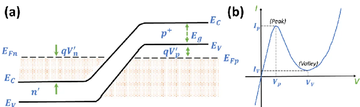
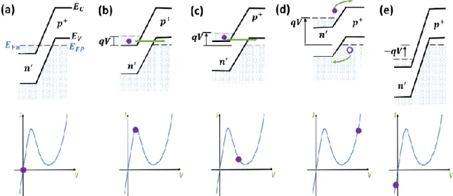
Ferroelectric Tunnel Junction memory (FTJ)
FTJ memory is a resistance based memory. It is composed of one ferroelectric ultrathin layer sandwiched by two metal electrodes (Metal-Ferroelectric-Metal).39 FTJ memories rely on the tunneling electroresistance effect (TER effect)40 which induces an electrical resistive switching. This in turn gives place to the presence of two distinct electrical resistance states (high- and low- resistance state).14 At the beginning, it was believed that the origin of the TER effect in an FTJ memory was attributed to a mechanisms related to “Piezoelectric effects”, where the application of an electric field produces strain on the ferroelectric barrier and therefore changes in the barrier width which modifies the electrical charge transport. However, FTJ memory devices are designed to operate at low voltages in order to avoid the desestabilitation of the ferroelectric state; then the piezoelectric effects are clamped in ultrathin films. Recent studies on the effect of the ferroelectric polarization over the transport properties of an ultrathin ferroelectric layer sandwiched between two conductive electrodes suggests that the main mechanisms that causes the TER effect in an FTJ are related to: “Microscopic interfacial effects”, where the reversal of a ferroelectric polarization changes the position of the ions near the interfaces (metal/ferroelectric), affecting the chemical bonding between the atoms, leading to a change in electronic charge transport and/or “depolarizing-field effects”, where the reversal of the ferroelectric tunnel barrier induces changes in the barrier height of an electrostatic potential profile which results in a change of the electrical transport properties.
The tunneling current density in an FTJ depends exponentially on the thickness of the ultrathin ferroelectric barrier. Basically, the ferroelectric dipole orientation codes for high or low resistance state in the FTJ memory device.14 The difference between the high and low resistance state is known as the TER ratio. Its value is usually in the range of 10 to 100.41-43 However, a giant
TER ratio had been demonstrated in FTJ memories based on BiFeO3,19 PbTiO344 and BaTiO3.17
A crucial condition to fabricate FTJ memory devices is to achieve ferroelectricity in ultrathin film form.15-16 Non-centrosymmetric perovskite materials in their thin film form such as BaTiO
3,5, 45-46
BiFeO347-48 and PbTiO344 are well known for their outstanding ferroelectric properties. However,
their ferroelectricity starts to disappear as their layer thickness decreases.15-16 For many years, it
thickness (around 10 nm).49 Recently, strain engineering studies had proved that the ferroelectricity is compatible with ultrathin films.49 This is possible, due to the strain forces generated between the film and substrate which distort the crystal structure lattice of the ultrathin film.49 This in turn reduces the symmetry of the crystal structure, which enhances the ferroelectricity in the ultrathin films. In 2009, Vincent Garcia et. al.17 made the experimental
demonstration of robust ferroelectricity in a 1-nm thick highly strained BaTiO3 film. This
discovery allowed the experimental demonstration of the tunneling electroresistance effect in a metal-ferroelectric-semiconductor structure. Up to know, perovskite materials such as BaTiO3,17, 43 PbTiO3,44 BiFeO319 and Pb(Zr,Ti)O331 have been successfully used as ultrathin
ferroelectric barriers in FTJ devices (Table 2).
Table 2. Survey of reported FTJs
Bottom (BE) and top (TE) electrode
Ferroelectric barrier
Deposition
technique Main remarks Ref.
BE=La0.67Sr0.33MnO3,
TE= Cr/Pt
BaTiO3
(tF=1nm)
TS= 775oC
PLD Ferroelectricity in 1 nm highly strain BaTiO
3 [17] 2009 BE= Nb:SrTiO3 BE= Au/ti BaTiO3 (tF=10u.c.) TS= 775oC
PLD TER effect demonstration 2009 [43] BE=SrRuO3
TE=conductive tip
PbTiO3
(tF=3.6nm)
TS= 700oC
PLD Giant TER effect FE of Retention of 72 h 2010 [44] BE=La0.67Sr0.33MnO3
TE=Co/Au
BaTiO3
(tF=2nm)
TS= 700oC
PLD TER ratio= 64 ON/OFF cycles=900 2012 [20] BE=Au/Co,
TE=La0.67Sr0.33MnO3
PZT* (tF=1.6nm)
TS= 700oC
PLD TER ratio= 300 at ±0.4V Brinkman model 2012 [31] BE=Ca0.96Ce0.04MnO3 TE= Co BiFeO3, (tF=4.6nm) PLD TER ratio = 103, ON/OFF cycles=106 [18] 2014 BE=Ca0.96Ce0.04MnO3 TE= Co/Pt BiFeO3, (tF=7u.c.) TS= 750oC PLD TER ratio = 10 4, Retention= 68 h, ON/OFF cycles=103 [19] 2013 BE=La0.67Sr0.33MnO3, TE= Graphene BaTiO3, (tF=6u.c.) TS= 680oC PLD TER ratio= 6000 at ±0.2V 2014 [50] BE=La0.67Sr0.33MnO3 TE= Cu BaTiO3, (tF=3nm) TS= 700oC PLD TER ratio of 1000 Brinkman model 2014 [51]
u.c.: Unit cell, PLD: Pulsed laser deposition, ALD: Atomic Layer deposition, TER: tunnelling electroresistance, *PZT: PbZr0.2Ti0.8O3,
The top and bottom electrodes in an FTJ device also play an important role52 because in principle, they define the quality of the ultrathin film morphology, ferroelectric behavior of the
tunnel barrier, TER ratio, and the electrical charge transport at the metal/ferroelectric interface.16, 30 In order to obtain a large TER ratio, the use of semiconductor materials as bottom
electrodes is required. This is, because they allow to barrier width to experience modulation to a greater extent by realizing a depletion region in the semiconductor near the ferroelectric/semiconductor interface. Also, it is required that the structural properties (crystal structure and cell size) of the bottom electrodes should be similar to the structural properties of the ultrathin film. When the ferroelectric layer of an FTJ is made of an oxide layer such as Hf0.5Zr0.5O2
the size of the TER ratio will be affected by the grade of crystallization of the film, when a large percentage of the grains that composed this oxide layer will results in a large TER ratio. Inversely, an oxide film composed mostly of non-crystalline grains will lead to issues in the TER ratio.53 As shown in Table 2, semiconductors such as La0.67Sr0.33MnO3 (3.871 Å),17 SrRuO3 (3.905 Å)44 and
Ca0.96Ce0.04MnO3 (3.946 Å)18 are used as bottom electrodes in FTJ devices based on
BaTiO3 (3.992 Å).
Recently, it was believed that in order to obtain coherent-direct tunneling current across the ferroelectric layer it was mandatory to use electrodes made of different materials.42 As they create an electrostatic potential barrier profile with a trapezoidal shape. This kind of shape allows coherent-direct tunneling current in FTJ devices.30 On the other hand, there should not be coherent-direct tunneling in an FTJ device which has same material in the top and bottom electrode. However this is not entirely true, as experimental evidence have shown that that the symmetry in an electrostatic potential profile can be broken. This loss in symmetric can come due to different reasons such as presence of different interface terminations, pinned interface dipoles or due to the formation of an ultrathin dielectric layer at one of the interfaces.14
2.3 THIN FILM GROWTH PROCESS
In the deposition process there are four steps involved: i) Production of the appropriate atomic, molecular or ionic species; ii) transport of these species from the source to the substrate; iii) condensation of the species on the substrate surface; and iv) nucleation, in which the adsorbed species interact among themselves to form clusters or nuclei. Once these nuclei reach a certain critical size, the clusters become thermodynamically stable.54 The growth process consists of a statistical process of nucleation, surface-diffusion, controlled growth of the three dimensional nuclei and its subsequent filling to give a continuous film.55 Depending on the thermodynamic
parameters of the deposit and substrate surface, the initial nucleation and growth stage can be described with three different growth modes:
i) Volmer-Weber or island growth occurs when stable clusters nucleate on the substrate surface and grow into three-dimensional island features (Figure 3). In this growth mode, the bonds of the atoms or molecules to be deposited are stronger between them than to the substrate material. Volmer-Weber growth mode is usually presented when the structural properties and the chemical composition of the substrate and the film are different.5,55
Figure 3. Volmer-Weber (island) growth. Adapted from ref. [55]
ii) Frank-Van der Merwe or “layer by layer” occurs when the atoms or molecules
deposited have the tendency to expand into two dimensions, which results in the formation of planar layers (Figure 4). This growth mode is characterized by a weak bonding forces between the deposited species (either molecules or atoms) and the strong bonding force between substrate atoms. An example of this growth mode is the epitaxial growth of semiconductors.5,55
iii) Stranski-Krastanov mode is a combination of the layer-by-layer and island growth modes. This mechanism occurs in two steps. First is the formation of one or more monolayers in a layer-by-layer mode, and the subsequently formation of islands on the top of the monolayers (Figure 5).5,55
Figure 5. Stranski-Krastanov growth. Adapted from ref. [55]
There are thermodynamic models for nucleation and growth of thin films which describe the surface energies between the substrate and the film. One model that describes the process of atomic nucleation of a film on the substrate during vapor deposition is presented in Figure 6. In this model, the mechanical equilibrium between the components of interfacial tension and constitutive phases is described by Young’s equation.54-55It is used to understand better the three
types of growth modes
𝛾𝑠𝑣 = 𝛾𝑓𝑠+ 𝛾𝑓𝑣𝑐𝑜𝑠𝜃 (1) Where 𝛾 is the interfacial energy while s, f and v stand for substrate, film and vapor, respectively and the contact angle (wetting angle) is represented by 𝜃. 54-55
Figure 6. Atomistic nucleation process during the film growth. Adapted from ref. [55]
Island growth mode occurs when the wetting angle is much higher than zero (𝜃 > 0), in this growth mode the surface tension of the film exceeds the surface tension of the substrate. As the wetting angle gets closer to zero (𝜃~0) a layer by layer growth mode occurs. This type of growth mode is characterized for present small difference in surface energy between the film and
the substrate, in this conditions the film wets the substrate surface. In the case of the Stranski-Krastanov growth, first the wetting angle is close to zero (𝜃~0) which leads to a layer-by-layer growth mode and after the island growth mode (𝜃 > 0) occurs. 54-55
There are two types of epitaxial growth. The first is known as homoepitaxy, it occurs when the material of the film to be deposited is the same as the material of the substrate (e.i. silicon film on a silicon substrate, Figure 7 (a)). The second epitaxial growth mode is known as heteroepitaxy, which occurs when the materials of the film and substrate are different. When the lattice parameters are slightly mismatched, strain-layer epitaxy growth mode occurs (Figure 7 (b)). The existence of large lattice mismatch between film/substrate (the crystal structure of the film and substrate are different) leads to the relaxation of the film material to its bulk structure through the formation of lineal defects such as dislocations (Figure 7 (c)). 54-55
Figure 7. Schematic representation of (a) a nearly lattice matched, (b) a strained and (c) a relaxed heteroepitaxial film growth. from ref. [54]
2.4 POLARIZATION PROPERTIES
A dielectric material is essentially an electrical insulator. However, under the application of an electric field the electrical charges shift from their equilibrium position resulting in a dielectric polarization (Figure 8).
Figure 8. Polarization of a dielectric crystal.
Among the different dielectric materials, non-linear dielectrics possess special properties such as: piezoelectricity, pyroelectricty and ferroelectricity. Based on the lattice structure and crystal symmetry they can be classified into 32 crystal classes (Figure 9). The application of mechanical stresses on a piezoelectric crystal leads to changes in crystal shape and in the centers of gravity of the charges (electrical polarization of the crystal). Piezoelectricity only appears in crystals that lack a center of symmetry. Among the different crystal classes only twenty-one correspond to the non-centrosymetric group, where just one of them cannot produce a dipole moment (cubic class 432). From the twenty remaining classes only ten are pyroelectric. This type of crystals are characterized for present spontaneous polarization when they are exposed to a certain temperature. Finally, among this ten crystal classes only a small fraction are ferroelectric. In this case, the spontaneous polarization occurs when the crystal is exposed to an electric field.
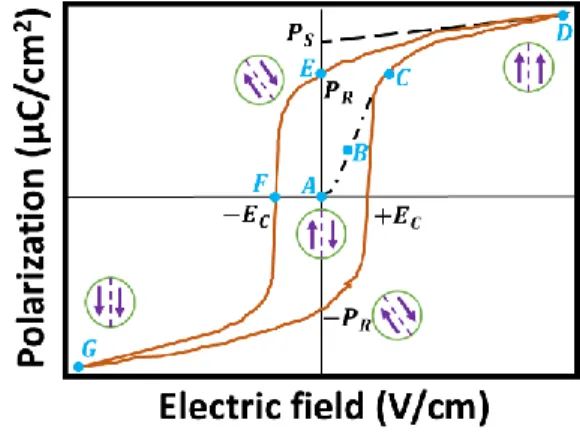
Ferroelectricity
Considering a crystal with several polarization domains aligned randomly, it will present an initial net polarization equal to zero in thermodynamic equilibrium (Point A, no application of voltage, Figure 10). However, the alignment of the polarization domains starts when a positive electric field is applied. In the small voltage regime, the polarization of the crystal increases linearly (Path AC). As the electric field increases (Path CD), the polarization domains will continue aligning until they reach a point of saturation (Point D). The value of spontaneous
polarization (PS) can be estimated by extrapolating the point of saturation limit to the “Y” axis. If the applied electric field is gradually removed, the net polarization will remain different of zero (Path DE), this value of polarization is known as remnant polarization (PR). The polarization of
the crystal can be removed if the direction of the electric field is changed (Path EF). The coercive
field (Ec) value can be regarded as the required energy to bring the polarization to zero. The
continue increase in the reverse field results in the complete reverse of the polarization (Path FG).
A negative remnant polarization value (-Pr) is obtained when the reverse electric field is gradually
removed. The formation of a complete polarization hysteresis loop occurs when a positive electric filed is applied again.56
Figure 10. Ferroelectric Polarization-Electric field hysteresis loop. Adapted from ref. [56]
Piezoelectricity
The application of a mechanical force on a piezoelectric crystal leads to a generation of electrical charges (direct piezoelectric effect). Conversely, an electric field applied induces mechanical strain in a piezoelectric crystal (converse piezoelectric effect).57,56
The relationship between mechanical strain and the resulting electrical polarization is known as the direct piezoelectric effect which is described by the following equation
𝑃𝑖 = 𝑑𝑖𝑗𝑘𝜎𝑗𝑘 (2)
Where the electrical polarization is denoted by 𝑃𝑖; the direct polarization coefficients and the stress are represented by 𝑑𝑖𝑗𝑘, and 𝜎𝑗𝑘, respectively. In the converse piezoelectric effect, the strain generated in a piezoelectric crystal is related to the applied electric field (E), where the transposed matric is denoted by t. 57,56
𝑠𝑖𝑗 = 𝑑𝑖𝑗𝑘𝑡 𝐸𝑘 (3)
In addition to the polarization-electric field hysteresis loop, the strain-electric field hysteresis loop is presented in Figure 11, which resembles the shape of a butterfly. When the electric field is equal to zero, the strain in the crystal will be zero (Point A). The crystal will expand upon the application of a positive electric field (piezoelectric effect (Eq. 2), path ABC). Point C
can be seen as the maximum expansion of the crystal (under the application of an electric field). As the electric field is gradually removed, the strain will trace a line from point C to A (strain equal to zero). The reverse of the electric field (negative direction) leads to reach the point D, in this point the strain jumps from point D to E and then moves along the segment E-F upon an increase of the negative electric field. The remove of the reverse electric field leads to reach the point A. Finally, the strain-electric field hysteresis loop is completed when a positive electric field is applied again (point G).
2.5 SOLID SOLUTION HAFNIUM ZIRCONIUM OXIDE
Hafnia (HfO2) and zirconia (ZrO2) are occasionally referred as twin materials since both
have similar properties. Under standard temperature and pressure conditions they have the same color (white), similar dielectric permittivity (𝜀~25), similar optical band gap (𝐸𝑔~5 𝑒𝑉) and also similar melting points (𝑇𝑀~ 2600℃). The resemblance is attributable to the structural similarity between the both oxides.59 Hafnium and zirconium elements belong to group four of the periodic table. Therefore, their ionic radii is almost similar (ionic radii for Hf4+ and Zr4+ are 0.78 Å and 0.79 Å, respectively).1 This similarity allows them to be completely miscible in the solid state as shown in Figure 12. The monoclinic phase is the equilibrium phase for both structures at low temperatures, while the tetragonal and cubic phases predominate at higher temperatures. These two elements are difficult to separate and in some cases some residues of zirconium can be find in hafnia.60-62
Structural properties of HfO2 and ZrO2
The schematic representation of the units cells for both different materials (ZrO2 and HfO2
systems) are presented inTable 3. As stated above, both materials present three different phases. The stable alpha phases (𝛼 − 𝐻𝑓𝑂2 and 𝛼 − 𝑍𝑟𝑂2) are monoclinic at temperatures below
~1800℃. As the temperature increases to higher temperatures both materials transform to beta phase (𝛽 − 𝐻𝑓𝑂2 and 𝛽 − 𝑍𝑟𝑂2), in this state they present a tetragonal crystal structure. At even
higher temperatures both oxides (𝛾 − 𝐻𝑓𝑂2 and 𝛾 − 𝑍𝑟𝑂2) transform into a cubic crystal
structure.29, 62
Table 3. Structural properties of HfO2 and ZrO2. from ref. [53]
Monoclinic (α-phase) Tetragonal (β-phase) Cubic (γ-phase)
ZrO2: a=5.15Å, b=5.20Å, c= 5.32Å and β=80o (below 1170oC)
ZrO2: a=5.09Å and c=5.18Å
(1171oC to 2369oC)
ZrO2: a=5.12Å
(above 2370oC) HfO2: a=5.15Å, b=5.19Å, c= 5.33Å
and β=99.6o (below 1827oC)
HfO2:a=3.59Å and c=5.22Å
(1828oC to 2520oC)
HfO2: a=5.14Å
(above 2521oC)
Ferroelectric properties of hafnium zirconium oxide (Hf0.5Zr0.5O2) film
Hafnia (HfO2) and zirconia (ZrO2) films combine excellent dielectric properties (𝜀~30)
with a relative low deposition temperature (typically 500oC).1, 4 These advantages makes them suitable for integration into the complementary metal oxide semiconductor (CMOS) process.26, 63-64 Indeed, the current generation of semiconductor memories uses high dielectric materials such as hafnia and/or zirconia films as dielectric layers for the fabrication of DRAM memory devices. Their implementation enables the increase of the gate capacitance without decreasing their physical thickness.1, 4
Another interesting property of hafnia-based zirconium films is their ferroelectric property. Even though, hafnia and zirconia have been studied for more than a century, it was just recently that its ferroelectric behavior was discovered. Indeed, just six years ago (2011) Muller et al.65-66
reported robust ferroelectricity in an ultrathin Hf0.5Zr0.5O2 film (~7.5 nm in thickness). The
coercive field of about 0.8MV/cm) with deposition parameters compatible with the CMOS process make it an excellent candidate to be used as a ferroelectric layer in an FTJ memory.
The origin of the ferroelectricity in Hf0.5Zr0.5O2 relies on the martensitic transformation
from tetragonal phase to an orthorhombic phase. It occurs during the initial stages of Hf0.5Zr0.5O2
film growth. First, it starts with the nucleation of small Hf0.5Zr0.5O2 grains with a high surface-to-
volume ratio, which results in the formation of a tetragonal phase (P42/nmc). However, the
combination of small compressive stress (along a- and b- axis) and a large tensile strain along the c-axis induced by the coalescence of the nucleating grains leads to the formation of the ferroelectric orthorhombic phase (Pbc21). The lattice parameters of the Hf0.5Zr0.5O2 orthorhombic phase
(𝑃𝑏𝑐21) are a=5.01Å, b=5.05Å and c=5.25Å.22, 53, 66
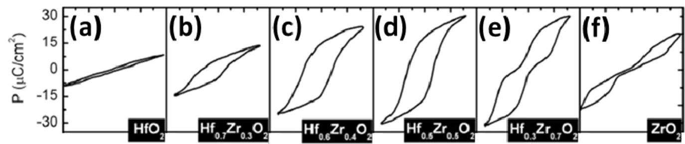
Hafnia and zirconia are completely miscible. However, ferroelectric behavior only appears when the molar percentages of zirconium and hafnium are around 50 % (Figure 13).21, 26, 67 Pure
hafnia in thin film form presents a centrosymetric monoclinic phase (𝐹𝑚3̅𝑚). The high symmetry of the crystal structure prevents ferroelectricity, therefore it shows paraelectric behavior in a
polarization vs voltage curve (Figure 13 (a)). On the other hand, pure zirconia in thin film form presents a non-centrosymetric tetragonal phase (P42/nmc), which surprisingly has antiferroelectric
nature (Figure 13 (e) and (f)). Hafnium-rich films exhibit predominantly monoclinic phase, which shows a certain degree of ferroelectricity (Figure 13 (b) and (c)), whereas Zirconium-rich films crystallize into a tetragonal phase (Figure 13 (e)). For films with a 50 molar percent of zirconia and 50 molar percent of hafnia, a non-centrosymetric orthorhombic (𝑃𝑏𝑐21) phase is formed, it presents ferroelectric properties (Figure 13 (d)).26
Figure 13. Evolution of the ferroelectric properties as a function of zirconium atomic concentration. Adapted from ref. [26]
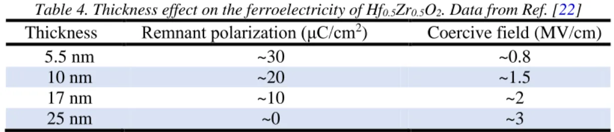
Contrary to conventional ferroelectric materials, where the ferroelectricity disappears below a certain thickness (~2 nm), in Hf0.5Zr0.5O2 the ferroelectricity disappears above a critical
thickness (~17 nm) and gets and improvement when the thickness is reduced.22 The effect of film thickness on the ferroelectricity of Hf0.5Zr0.5O2 is presented in Table 4.
Table 4. Thickness effect on the ferroelectricity of Hf0.5Zr0.5O2. Data from Ref. [22] Thickness Remnant polarization (μC/cm2) Coercive field (MV/cm)
5.5 nm ~30 ~0.8
10 nm ~20 ~1.5
17 nm ~10 ~2
25 nm ~0 ~3
*Metal-Insulator-Metal structure= SiO2/TiN-Hf0.5Zr0.5O2-TiN
The solid solution Hf0.5Zr0.5O2 can be produced via different deposition techniques
(Table 5). Techniques such as atomic layer deposition, plasma-enhanced atomic layer and sol-gel
enable the deposition of Hf0.5Zr0.5O2 films at low substrate temperature (280oC). However, the
as-deposited film is not crystalline, therefore it does not have ferrroelectric properties. Table 5. Survey of experimental reports on Hf0.5Zr0.5O2.
Substrate Deposited layer Deposition technique Main remarks Ref
Silicon Zr doped HfO2
10- 90 at. % MALD (TS=500oC,TA=600oC) HZO dielectric properties [68] 2009 Silicon Hf1−XZrXO2 X= 0-1 at. % PALD (TS=280oC, TA =950oC) HZO structural properties [29] 2010 TiN Hf0.5Zr0.5O2 ALD (TS=280oC, TA =550oC) Thermal cycles on HZO films [69] 2013 Pt Hf0.5Zr0.5O2 Sputtering (TS=500oC, TA =---oC) Charge-trapping memory [67] 2014 TiN Hf0.5Zr0.5O2 tF= 12-60 nm Sol–gel method (TS=--oC, TA =700oC) Synthesis by a wet technique [70] 2015
HZO stands for Hf0.5Zr0.5O2, MALD (Metalorganic atomic layer deposition), PALD (Plasma-enhanced atomic-layer)
To crystallize the as-deposited film, it is necessary to apply a thermal treatment at relative high temperatures (450-950oC).29, 68-70 However, RF-magnetron sputtering can produce crystalline
Hf0.5Zr0.5O2 films in one single step. Indeed, Lu et al. reported in 2014, the crystallization of an
ultrathin Hf0.5Zr0.5O2 films by RF magnetron sputtering.67 In the present work, the deposition of
Hf0.5Zr0.5O2 films is achieved by RF-Magnetron sputtering as it offers many advantages such as
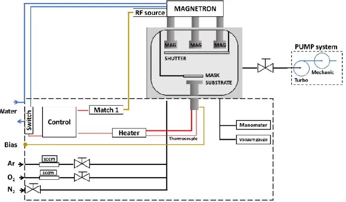
crystallization of materials at low temperatures, control of the deposition rate, uniform deposition over relative large areas (1 × 1 𝑐𝑚) as well as an easy scaled-up.
2.6 ELECTRONIC CHARGE TRANSPORT AT THE SEMICONDUCTOR INTERFACE
In FTJ devices, the electron current flow across the whole device is defined by the width and shape of the electrostatic potential profile.30,52 In semiconductor memory device technology,
the charge transport at the interfaces is one of the most important properties and it has become an essential issue of modern electronic device design.14
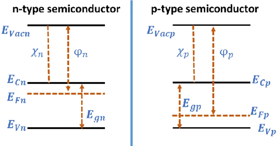
Heterostructures
Semiconductors have an energy level diagram as the shown in Figure 14. The distance between valence band (EV) and the conduction band (EC) is known as band gap (Eg). Fermi level
(EF) is placed inside of the band gap. The electron affinity (χ) is the energy difference between the
vacuum level and the conduction band (EC) while the work function (φ) is the distance between
vacuum level and the Fermi level.71
Figure 14. Typical energy band diagram for a semiconductor. Adapted from ref. [71]
The energy-band diagram of a semiconductor p-type and n-type in non-contact (neutral state) are presented inFigure 15. The junction of both semiconductors leads to a changes at the interface. Band line up of their energy band will occur until the alignment of the Fermi levels energy of both semiconductors is reached. In this process, the electrons flow from the semiconductor with the higher Fermi level to the semiconductor with the lower Fermi level. This electron transfer is compensated by the built up of an electric field.71
Figure 15. Energy band diagram for n- and p-type semiconductors in non-contact. Adapted from ref. [71] These heterostructures can be classified into three categories (Figure 16): Type-I (straddling), where one of the semiconductors presents both lower conduction band energy (EC)
and higher valence band energy (EV), as well as a smaller energy band gap (Eg). Type-II (staggered)
occurs when the conduction (EC) and the valence (EV) band energies of one the semiconductors
are lower respect to the conduction (EC) and valence band (EV) of the other semiconductor,
respectively. Type-III (broken-gap) here the conduction band energy (EC) of one of the
semiconductors is lower than the valence band energy (Ev) of the other.71
Figure 16. Classification of the hetostructructures: Type I (Straddled), Type II (Staggered) and Type III (Broken gap). Adapted from ref. [71]
![Table 1. Memory hierarchy and memory properties. Data obtained from ref. [7]](https://thumb-eu.123doks.com/thumbv2/123doknet/5005060.124757/20.918.107.821.378.658/table-memory-hierarchy-memory-properties-data-obtained-ref.webp)
![Figure 12. Phase diagram of the binary system HfO 2 -ZrO 2 . Adapted from ref. [62]](https://thumb-eu.123doks.com/thumbv2/123doknet/5005060.124757/36.918.318.656.631.989/figure-phase-diagram-binary-hfo-zro-adapted-ref.webp)
![Figure 23. Interpretation of the X-ray reflectometry data. Adapted from ref. [76]](https://thumb-eu.123doks.com/thumbv2/123doknet/5005060.124757/51.918.296.675.601.913/figure-interpretation-x-ray-reflectometry-data-adapted-ref.webp)
