HAL Id: tel-00084018
https://tel.archives-ouvertes.fr/tel-00084018
Submitted on 5 Jul 2006
HAL is a multi-disciplinary open access
archive for the deposit and dissemination of sci-entific research documents, whether they are pub-lished or not. The documents may come from teaching and research institutions in France or abroad, or from public or private research centers.
L’archive ouverte pluridisciplinaire HAL, est destinée au dépôt et à la diffusion de documents scientifiques de niveau recherche, publiés ou non, émanant des établissements d’enseignement et de recherche français ou étrangers, des laboratoires publics ou privés.
AMELIORATION DES PERFORMANCES DES LASERS A CASCADE QUANTIQUE - ETUDE DU CONFINEMENT OPTIQUE ET DES PROPRIETES
THERMIQUES
Jean-Yves Bengloan
To cite this version:
Jean-Yves Bengloan. AMELIORATION DES PERFORMANCES DES LASERS A CASCADE QUANTIQUE - ETUDE DU CONFINEMENT OPTIQUE ET DES PROPRIETES THERMIQUES. Physique Atomique [physics.atom-ph]. Université Paris Sud - Paris XI, 2005. Français. �tel-00084018�
Amélioration des performances des Lasers à Cascade Quantique :
Étude du confinement optique et des propriétés thermiques
Thèse effectuée à Thales Research & Technology (TRT) à l’Université de Paris VII
J-Y Bengloan
Performance optimisation of Quantum Cascade Lasers:
Investigation of the optical confinement and thermal properties
J-Y Bengloan
Thèse effectuée à Thales Research & Technology (TRT) Thèse de doctorat de l’Université de Paris XI – Sud (Orsay)
3
PLAN
1. Introduction
2. Waveguide Optimisation in GaAs/AlGaAs QCLs
GaAs based guides (plasmon enhanced) / Limitations AlGaAs and GaInP Guides
3. Enhancement of thermal dissipation properties of GaInAs/AlInAs/InP
QCLs
Selective current injection by proton implantation Thick electro-plated gold
Quantum Cascade Lasers (QCLs)
• INTERSUBBAND transitions
• UNIPOLAR : only one type of carrier used (e-)
Main Properties
Main Properties
hν e -CB Distance (z) Energy5
45 nm
Quantum Cascade Lasers (QCLs)
Active Region (AR) grown by Molecular Beam Epitaxy (MBE)
"MINIGAP"
Transport zone Emission zone
3 2 1
e
-"MINIBAND" "MINIGAP"Transport zone Emission zone
3 2 1
e
-e
-"MINIBAND" • CASCADE scheme : Recycling of carriersSpectral range of QCLs
InP/GaInAsP Wavelength (µm) 0 5 10 15 20 25 100 0.5 1 1.5 2 Classic Laser DiodesGaN/AlInGaN GaAs/GaInAsGaAs/AlGaInP
GaSb PbSe (cryo)
UV Near IR
THz
Mid IR Far IR
Quantum Cascade Lasers
GaInAs/AlInAs/InP ; GaAs/AlGaAs ; InAs/AlSb
3.5 µm < λ < 24 µm and λ> 65 µm
Applications:
• Spectroscopy and high sensitive Gas detection Environmental, Medical, Security
• Free space optical communication
7
QCL History
1994 QCL in GaInAs/AlInAs/InP QCL in GaAs/AlGaAs 2003 1998 2002 QCL in InAs/AlSb Room temperature CW operation for GaInAs/AlInAs/InP QCL 2005 150K CW operation QCL in GaAs/AlGaAs QCL 400mW room temperature CW operation for GaInAs/AlInAs/InP QCL CW: Continuous WaveFrom intersubband emission
to CW laser operation
First Laseroperation operationFirst CW
Pulsed operation CW operation Gain optimisation
78K
78K 78K 300K
Waveguide design optimisation
Thermal management Quantum engineering of Active Region
9
Thesis S.Barbieri - C.Becker
From intersubband emission
to CW laser operation
First laseroperation operationFirst CW
Pulsed operation CW operation Gain optimisation 78K 78K 78K 300K InP-based QCL 1994 (Bell Labs) 2002 (Neuchâtel) 1995 (80K) (Bell Labs)
Waveguide design optimisation
Heat dissipation management Quantum engineering of Active Region
1998
(Thales)
GaAs/AlGaAs
QCL 2000 (30K)(TU Wien)
Waveguide design optimisation
PLAN
1. Introduction
2. Waveguide Optimisation in GaAs/AlGaAs QCLs
GaAs based guides (plasmon enhanced) / Limitations AlGaAs and GaInP Guides
3. Enhancement of thermal dissipation properties of GaInAs/AlInAs/InP
QCLs
Selective current injection by proton implantation Thick electro-plated gold
11
Pulsed operation QCL devevopment:
Reduction of the threshold current density J
thJth = (αwg+ αm) / g Γ QCL J AR J Optical power Jth
Waveguide design optimisation : αwg, Γ Quantum engineering of Active Region : g
0 5 10 15 20 25 1998 2000 2002 year J th (kA/cm²) 300K 78K GaAs based QCL
Waveguide principle
n2 > n1≥n3 n1 n3 Cladding n2 Core n1 Cladding n2Guiding condition : n
1> n
2Increase figure of merit
χ= Γ / α
wWaveguide optimisation by numerical simulations :
• 1D Simulations : Transfer Matrix Method (TMM)
choice of
appropriate layer
compositions and
thicknesses
Decrease
J
th=(
α
w+α
m)/g
Γ
13
Current GaAs QCL waveguides (1)
GaAs Plasmon enhanced waveguide with highly doped cladding layers
neff=3.19 α = 17 cm-1 Γ = 28% λ = 9.4µm
χ= 1.7
J
th=15kA/cm
2 Distance (µm) -12 -10 -8 -6 -4 -2 0 0 0.2 0.4 0.6 0.8 1Optical intensity (a.u.)
0 2 4 6 8 10 Refractive index AR n+ n+ GaAs GaAs n- n -èAdvantages
l straight-forward MBE growth l good electrical characteristics
èDrawbacks
l free carrier absorption (FCA) losses
Vertical dimension (µm) -12 -10 -8 -6 -4 -2 0 0 0.2 0.4 0.6 0.8 1
Optical intensity (A.U.)
0 2 4 6 8 10 Refractive index Active Region LOC LOC Plasm. Plasm.
Normalised optical intensity
(a.u)
Distance (µm)
Refractive
index
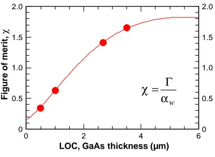
LOC=0,5; α=177cm-1; Γ=63%; χ=0,4
Normalised optical intensity
(a.u)
Distance (µm)
Refractive
index
LOC=1; α= 92,5 cm-1; Γ=58%; χ=0,6
Normalised optical intensity
(a.u)
Distance (µm)
Refractive
index
LOC=2,6; α=25 cm-1; Γ=35%; χ=1,4
Normalised optical intensity
(a.u.) Distance (µm) Refractive index LOC=3,5 ; α=17cm-1; Γ=28%; χ=1,7 0 0.5 1.0 1.5 2.0 0 2 4 60 0.5 1.0 1.5 2.0
LOC, GaAs thickness (µm)
w α χ = Γ
Figure of merit,
χ
Current GaAs QCL waveguides (2)
The χ optimisation is a trade-off between : • Γ, decreasing with the GaAs thickness
15
Dielectric waveguide optimisation
NECESSITY TO REDUCE OPTICAL LOSSES FROM CLADDINGS
è Plasmon enhanced waveguide
strengthened by dielectric layers :
q
AlGaAs layersq
GaInP layers -12 -10 -8 -6 -4 -2 0 0 0.1 0.2 0.3 -12 -10 -8 -6 -4 -2 0 2 2.5 3 3.5 hGaAshDIEL Refractive index
Distance (µm)
Normalised optical intensity (
a.u
)
AR
n+ n+
DIELECTRIC
DIELECTRIC Maximum growth thickness ~10µm
1 2 3 4 0 1 2 3 0 1 2 3 Figure of merit, χ hGaAs(µm)
−
x=20%−
x=36%−
x=70%−
x=94% hAlGaAs(µm) GaAs waveguide -12 -10 -8 -6 -4 -2 0 0 0.1 0.2 0.3 -12 -10 -8 -6 -4 -2 02 2.5 3 3.5 hGaAshAlGaAs Refractive index
Distance (µm)
Normalised optical intensity (
a.u. ) AR n+ n+ AlGaAs AlGaAs
Al
xGa
1-xAs cladding waveguides
With xAl Þ:⇒
∆nGaAs/AlGaAsÞ⇒
Γ Þ17
Al
xGa
1-xAs cladding waveguides
-12 -10 -8 -6 -4 -2 0 0 0.1 0.2 0.3 -12 -10 -8 -6 -4 -2 02 2.5 3 3.5 hGaAshAlGaAs Refractive index
Distance (µm)
Normalised optical intensity (
a.u ) AR n+ n+ AlGaAs AlGaAs
Limitations : lattice mismatch constraint â Al
xGa
1-xAs thickness limit ~1/x
Al!
1 2 3 4 0 1 2 3 0 1 2 3 Figure of merit, χ hGaAs(µm)−
x=20%−
x=36%−
x=70%−
x=94% hAlGaAs(µm) GaAs waveguide With xAl Þ:⇒
∆nGaAs/AlGaAsÞ⇒
Γ ÞAl
0.94Ga
0.06As cladding waveguides / QCL AL94
χ=2.9
è Jth ~2 times smaller than that of the GaAs plasmon enhanced waveguide.
Al0.94Ga0,06As cladding waveguide
Normalised optical intensity
(a.u.) Distance (µm) Refractive index α=12cm-1; Γ=35%; χ=2,9 20 µm I H+implantation (insulating)
2 devices grown and processed identically: èGaAs : GaAs waveguide
èAL94 : Al0.94Ga0.06As waveguide
• Identical 3 quantum-well AR ( same growth set ) • Double trench ridge devices
• H+ implanted for selective current channelling • Low duty cycle to avoid device heating
19 0 0.2 0.4 0.6 0 5 10 15 20
Optical peak power (W)
Current density (kA/cm²)
200K 240K 200K 240K 300K
−
AL94 − −GaAsQCL AL94
5kHz-100nsGood optical performances for QCL AL94:
è Significant reduction of Jth
è Agreement with simulations:
Jth(GaAs) / Jth(AL94) ≅ χ(AL94) / χ(GaAs)≅ 2 è Higher optical peak power
0 0.2 0.4 0.6
0 5 10 15 20
Optical peak power (W)
Current density (kA/cm²)
200K 240K 200K 240K 300K
−
AL94 − −GaAsQCL AL94
5kHz-100nsGood optical performances for QCL AL94:
è Significant reduction of Jth
è Agreement with simulations:
Jth(GaAs) / Jth(AL94) ≅ χ(AL94) / χ(GaAs)≅ 2 è Higher optical peak power
è 300K operation 0 5 10 15 20 25 30 0 1 2 3 4 5 T=240K Bias (V) Current (A)
−
AL94 − − GaAsPoor electrical characteristics for QCL AL94:
è Abnormally high knee: Vc=14V (Vc(GaAs)=5V)
Bad ohmic contacts?
Bad grading between GaAs and AlGaAs layers?
è Higher differential resistances
3x higher for AL94 device compared to GaAs QCL
21
Al
0.36Ga
0.64As cladding waveguides
Electrical conductivity better than Al0,94Ga0,06As layers:
better e- mobility lower effective mass
Al0.36Ga0.64As cladding waveguide
χ=2,5
Norm. optical intensity (
a.u. ) Refractive index Distance (µm) α=15cm-1; Γ=37%; χ=2,5 1 2 3 4 0 1 2 3 0 1 2 3 Figure of merit, χ hGaAs(µm)
−
x=20%−
x=36%−
x=70%−
x=94% hAlGaAs(µm) GaAs waveguideQCL AL36
5kHz-100ns
Good optical performances for QCL AL36:
è Jth significantly lower than Jth(GaAs) è Jth slightly higher than Jth(AL94)
è Higher optical peak power Pmax(AL36)=250 mW at 300K
Electrical characteristics dependant on the temperature:
è Higher differential resistances
èdV/dI= f (T) for AL36 QCL: Eact=132meV è High operating voltage for T<260K
0 10 20 30 40 0 2 4 240K Bias (V) Current (A) AL94 AL36 GaAs 260K 280K 300K 0 0.2 0.4 0.6 0.8 0 5 10 15
Optical peak power (W)
Current density (kA/cm²)
−
240K−
300K AL94 AL94 AL36 AL3623
Ø Ga0.51In0.49P refractive index ≅ Al0.45Ga0.55As refractive index
è Good ∆nGaAs/GaInP for improved confinement: χ=2,9
Ø Good electrical conductivity
Ø Ga0.51In0.49P : lattice matched to GaAs
è no thickness limitation
Ga
0.51In
0.49P cladding waveguides
Drawback : Ga0.51In0.49P re-growth by MOVPE at Thales χ=2,9 è growth in 3 stepsNorm. optical intensity (
a.u ) Refractive index Distance (µm) MBE MOVPE MOVPE α=13cm-1; Γ=38%; χ=2,9
QCL GaInP
5kHz-100ns
Good optical performances for QCL AL36:
è Jth significantly lower than Jth(GaAs) è Jth(GaInP) higher than Jth(AL36)
è High optical peak power at 78K Pmax(GaInP)=1,9W at 78K
è Optical peak lower than QCL AL36 at RT Pmax(GaInP)=150 mW at 300K 0 0.2 0.4 0.6 0.8 0 5 10 15 20
Optical peak power (W)
Current density (kA/cm²)
−
240K−
300K GaInP AL36 AL36 GaInP 0 0.5 1.0 1.5 2.0 0 5 10 15 20Optical peak power (W)
Current density (kA/cm²)
GaAs GaInP
−
GaInP− − GaAs
25
QCL GaInP
5kHz-100ns
Electrical characteristics :
è Higher knee bias: Vc=7V (Vc(GaAs)=5V)
è Lower differential resistance than AL36 è Higher operating voltage than GaAs
0 5 10 15 0 1 2 3 4 Bias (V) Current (A) GaInP AL36 GaAs T=300K 0 0.2 0.4 0.6 0.8 0 5 10 15 20
Optical peak power (W)
Current density (kA/cm²)
−
240K−
300K GaInP AL36 AL36 GaInPGood optical performances for QCL AL36:
è Jth significantly lower than Jth(GaAs) è Jth(GaInP) higher than Jth(AL36)
è High optical peak power at 78K Pmax(GaInP)=1,9W at 78K
è Optical peak lower than QCL AL36 at RT Pmax(GaInP)=150 mW at 300K
Reduction of threshold current densities:
è Low Jth
è Agreement with our predictions for AL94 and AL36:
Jth(GaAs) / Jth(Diel.)≅ χ(Diel.) / χ(GaAs)
Summary of laser performances
Better Wall-Plug efficiencies than LCQ GaAs
èWP(GaInP)=1%= 10xWP(GaAs) at 240K 0 0.2 0.4 0.6 0.8 1.0 0 1 2 3 4 5 Current (A) Wall -plug efficiency (%)
−
−
GaInPAL36−
AL94−
GaAs T=240K 0,1%Best waveguide device :
Best QCLs : QCL AL36 for T> 250 K Electrical degradations
>
Optical performances improvements 0 2 4 6 8 10 12 14 100 200 300 Jth (kA/cm²) T (K) GaAs GaInP AL36 AL94•
•
•
•
10kA/cm² 1%27
Waveguide loss measurements
0 5 10 15 20 -20 -10 0 10 20 αm (cm-1) Jth (kA/cm²) 300K 240K 180K 150K 78K
Waveguide losses αw determined from
Jth=f(αm) plot: Jth=(αm+αw)/gΓ αw=21cm-1 αw=12cm-1 QCL GaInP 21 cm-1 12 cm-1 GaInP 19 cm-1 -AL36 -20 cm-1 GaAs
α
w T≥180K T<180K Reduction of αw at low temperature compared to QCL GaAs αw increase at T ≥ 180K0 200 400 600 0 20 40 60 Energie (meV ) 3 2 1
Gain coefficient
Carrier leakage into the continuum ? Observation of 2 operating regimes
g ∝ τ3 ∝ exp(Eact/kT)
∆Eact=58meV
Carrier leakage into the continuum
Limitation of the conduction band discontinuity of GaAs/AlGaAs for room
temperature operation Jth=f(αm) plot _ gΓ =f(T) 2 4 6 8 0.002 0.004 0.006 0.008 0.010 0.012 g. Γ (cm / kA ) 1 /T (K-1) Eact=57.7meV Eact=53.2meV GaInP AL36
•
•
Arrhenius diagram29
Waveguide study conclusion
Best performances (Jth, Pmax) on GaAs-based QCLs
Limitation from the conduction band discontinuity of
GaAs/AlGaAs underlined for room temperature operation
Application of these waveguides on a bound-to-continuum AR QCL Significant reduction of Jth 0 5 10 15 20 25 1998 2000 2002 2004 2006 year J th (kA/cm²) 300K 78K GaAs based QCL
Degradation of the electrical transport
PLAN
PLAN
1. Introduction
2. Waveguide Optimisation in GaAs/AlGaAs QCLs
GaAs based guides (plasmon enhanced) / Limitations AlGaAs and GaInP Guides
3. Enhancement of thermal dissipation properties of GaInAs/AlInAs/InP
QCLs
Selective current injection by proton implantation Thick electro-plated gold
31
Application to InP-based QCLs
Minigap Miniband 1 2 3 4 Electron injection Electron extraction Miniband MinigapBeck et al., Science 295, 301, (2002)
Active Region: λ~9µm
4 Quantum Wells
Vertical Waveguide Structure: χ~12 Γ~69% α~6 cm-1
Normalised optical intensity
(a.u. ) Refractive index Distance (µm) AR n+ InP substrate InP
No lateral heat dissipation
Standard ridge waveguide
Good lateral heat flow
Buried heterostructure
InP InP based QCLsHeat management in QCLs
InP InP H+ implantationSelective current injection
33
Selective current injection
Lateral mode profile
W D Distance (µm)0 3 7 -7 -3 Intensity (a.u.)
0,5
14
6
D
W
≈
=
For
H+ implantation W DSemi-insulating layers using proton implantation
decrease electrically pumped area
⇒
Pumped area (A)
à
: -50%
⇒
Mode overlap (
Γ)
à
: -20%
⇒
J
th∝ 1/
Γ
Þ
: +20%
⇒
I
th= J
thx A
à
: -40%
Selective current injection in InP QCLs:
L-I-V pulsed characteristics
2 4 6 8 1 0 0 0.1 0 .2 0.3 0 .4 0.5 0 .6 0.7 0 .8 0.9 1 .0 0 1 2 3 4 5 6 7 8 0 0 .1 0 .2 0 .3 0 .4 0 .5 Voltage (V) Optical Power (W ) Current (A) T=78K
Current Density (kA/cm2)
5KHz - 100ns 0 2 4 6 8 10 0 0.5 1.0 1.5 0 1 2 3 4 5 6 7 8 9 10 11 12 0 0.1 0.2 0.3 0.4 0.5 Voltage (V) Optical Power (W ) Current (A) 320K 240K 260K 280K 300K
Current Density (kA/cm2)
@78K: Ith=135 mA, Jth=1,1 kA/cm² @300K: Ith=500 mA, Jth=4,3 kA/cm²
35 0 1 2 3 4 5 6 7 100 200 300 J th (kA.cm -2) T (K) T0=93K
T
0characteristics
T0 : Characteristic temperature from fit : Jth= Jth0 . exp(T/T0)LEAKS LEAKS 0 1 2 3 4 5 6 7 100 200 300 J th (kA.cm -2) T (K) T0=177K T0=93K InP without H+ InP with H+
•
•
SiO2 (Insulator) n-InP Contact (Gold)Standard ridge waveguide
Low T0
H+
Current leakage – implantation breakdown
Ileaks LCQ LCQ Active Region 0.1 0.2 0.3 100 2 00 30 0 10 20 50 Normalised resistance ( Ω .cm 2 ) Temperature (K) Resistance ( Ω ) Tact=1023K Eact=86meVH
+implantation creates shallow defects in n-doped InP material
H
+implantation
works well in
GaAs but not
in n-InP
E
cE
vGaAs
E
cE
vn-InP
37
Selective current injection for InP-based QCLs ?
Selective current injection by H+ implantation inefficient in InP-based QCLs
Fe doped InP
Future : use of Fe-doped InP as insulating layer - Deep defects in InP bandgap
CW operation for H
+implanted InP-based QCLs
4 6 8 10 0 0.2 0.4 0.6 0.8 1.0 1.2 0 100 200 300 400 Tension (V) Optical power ( mW ) Current (A) CW T = 78K 0 20 40 60 0 0.2 0.4 0.6 0.8 1.0 1.2 Optical power ( mW Current (A) CW 0°C 10°C 20°C 350 mW 18 mW 20°CHigh Temperature CW operation
even with current leakage
39
Electroplated Gold (Au) devices
24 µm Gold 20 µm SiO2
epi down
epi up
epi up
epi down + mirror
4 experimental arrangements:
Without Au With electroplated Au
L1 L2 L3 L4
Electroplated Au Device
Very good heat dissipation device
Best performances obtained on QCLs with this type of device Slivken et al, APL (2004)
Effect of Thick electroplated Au
0 50 100 150 200 0 10 20 30 40 50 60 70 Average optical power (mW) Duty cycle (%) T=10°Cepi up
L1P
max= 49mW for DC=12%
L1
41
Effect of Thick electroplated Au
0 50 100 150 200 0 10 20 30 40 50 60 70 Average optical power (mW) Duty cycle (%) T=10°C
epi up
L1 L2P
max= 49mW for DC=12%
L1
P
max= 78mW for DC=25%
L2
Effect of Thick electroplated Au
0 50 100 150 200 0 10 20 30 40 50 60 70 Average optical power (mW) Duty cycle (%) T=10°Cepi down
L1 L2 L3L1
P
max= 49mW for DC=12%
P
max= 102mW for DC=37%
L3
P
max= 78mW for DC=25%
L2
43
Effect of Thick electroplated Au
0 50 100 150 200 0 10 20 30 40 50 60 70 Average optical power (mW) Duty cycle (%) T=10°C
epi down
+ mirror
L1 L2 L3 L4P
max= 49mW for DC=12%
L1
P
max= 175mW for DC=40%
L4
P
max= 102mW for DC=37%
L3
P
max= 78mW for DC=25%
L2
Thick electroplated Au - Summary
epi down
+ mirror
epi down
epi up
epi up
L4
L3
L2
L1
R
th(K.cm/ W)
6
2,9
1,8
1,8
-50%
~ -40%
Buried Heterostructure
(Beck et al, Science295, 2002)
45
Thick electroplated Au - Summary
epi down
+ mirror
epi down
epi up
epi up
L4
L3
L2
L1
R
th(K.cm/ W)
6
2,9
1,8
1,8
Max. CW
temperature
_
130K
240K
278K
Buried Heterostructure
(Beck et al, Science 2002)
PLAN
PLAN
1. Introduction
2. Waveguide Optimisation in GaAs/AlGaAs QCLs
GaAs based guides (plasmon enhanced) / Limitations AlGaAs and GaInP Guides
3. Enhancement of thermal dissipation properties of GaInAs/AlInAs/InP
QCLs
Selective current injection by proton implantation Thick electro-plated gold
47
Conclusion
Use these waveguide on a bound to continuum structure
Thick electroplated Au on selective current injection devices
Breakdown of selective current injection (H+ implanted layers) in InP-based QCLs Significant performance improvements realised in GaAs-based QCLs owing
to waveguide optimisation
Application of Fe-doped InP layer
Significant thermal improvements realised with thick electroplated Au Rth close to that of buried heterostructure
Mid IR QCL Material ?
0 5 10 0 5 10 15 200 0.5 1.0 Voltage(V)Optical peak power (W
)
REF_GaAs
J (kA/cm2)
InP
T=78K GaAs has an intrinsic lower gain than GaInAs (m*>m*)
Increase in Jth Ioperation(Small dynamic current range)
Higher doping in the active region and the claddings Higher losses
49
Which material for which wavelength ?
0 100 200 300 400 2 5 10 20 Temperature (K) III-V compounds phonon bands LN2 Peltier Atmospheric windows 500 Wavelength (µm) 50 100
GaAs based lasers InP based lasers
200 Far Infrared (THz) : GaAs/AlGaAs QCLs Mid Infrared : AlInAs/GaInAs/InP QCLs InAs/AlSb QCLs
Contributions to this work…
Thesis directed by Carlo Sirtori
Epitaxy realised by: X. Marcadet (MBE)
M. Lecomte, O. Parillaud (MOVPE)
Devices processing: M. Calligaro, M. Carbonnelle
Y. Robert, C. Darnazian
Characterisations realised with the help of :
C. Faugeras, L. Sapienza, S. Forget, E. Boër-Duchemin