HAL Id: hal-03015338
https://hal.archives-ouvertes.fr/hal-03015338
Submitted on 19 Nov 2020HAL is a multi-disciplinary open access archive for the deposit and dissemination of sci-entific research documents, whether they are pub-lished or not. The documents may come from teaching and research institutions in France or abroad, or from public or private research centers.
L’archive ouverte pluridisciplinaire HAL, est destinée au dépôt et à la diffusion de documents scientifiques de niveau recherche, publiés ou non, émanant des établissements d’enseignement et de recherche français ou étrangers, des laboratoires publics ou privés.
co-reactive magnetron sputtering
Adriano Panepinto, Pierre-Antoine Cormier, Jonathan Dervaux, Mohammed
Boujtita, Fabrice Odobel, Rony Snyders
To cite this version:
Adriano Panepinto, Pierre-Antoine Cormier, Jonathan Dervaux, Mohammed Boujtita, Fabrice Odobel, et al.. Synthesis of p-type N-doped TiO 2 thin films by co-reactive magnetron sputtering. Plasma Processes and Polymers, Wiley-VCH Verlag, 2020, 17 (3), pp.1900203. �10.1002/ppap.201900203�. �hal-03015338�
Synthesis of p-type N-doped TiO
2thin films by
co-reactive magnetron sputtering
A. Panepinto1, P.-A. Cormier1, J. Dervaux1, M. Boujtita2, F. Odobel2 and R. Snyders1,3 1 Chimie des Interactions Plasma-Surface (ChIPS), Université de Mons, 23 Place du Parc,
7000 Mons, Belgium
2CEISAM, Université de Nantes, CNRS, 2 rue de la Houssinière, 44322 Nantes cedex 3, France 3Materia Nova Research Center, 3 Avenue Nicolas Copernic, 7000 Mons, Belgium.
Emails address: adriano.panepinto@umons.ac.be; pierre-antoine.cormier@umons.ac.be;
jonathan.dervaux@umons.ac.be; mohammed.boujtita@univ-nantes.fr;
fabrice.odobel@univ-nantes.fr; Rony.Snyders@umons.ac.be
Corresponding author: Panepinto Adriano, University of Mons, 20 Place du Parc, B-7000 Mons, Belgium, Tel: +3265554945, Fax: +3265554941, email:
Abstract
Tandem Dye-Sensitized Solar Cells devices (t-DSSCs) can theoretically overcome the well-known Shockley-Queisser limit due to their unique structure combining a n-type photoanode, a p-type photocathode and multiple dyes with complementary absorption characteristics. Nevertheless, nowadays, their further development suffers from the poor quality of the p-type material constituting the photocathode, i.e. NiO or Cu delafossites, and is therefore dependent of the synthesis of new efficient materials. In this work, N-doped TiO2 thin films exhibiting a p-type conductivity (p-TiO2:N) are successfully synthesized by co-reactive magnetron sputtering. The p-type conductivity is correlated to the incorporation of N atoms in substitutional positions which is shown to be controllable by carefully tuning the ratio between O2 and N2 reactive gases during the growth of the material. Furthermore, we show that if p-TiO2:N films present a lower hole concentration (~ 1015-1016 cm−3) and optical transmission in the visible (~ 36-40 %) than sputtered NiO, it reveals a 3 to 6 times higher mobility of the charge carriers (1.5 - 3.1 cm2.V−1.s−1). These results are in particular interest for the future development of new “full TiO2”-based t-DSSCs.
Keywords: tandem-DSSCs; N-doped TiO2; p-type semiconductor; reactive magnetron sputtering; GLAD.
1. Introduction
Dye-Sensitized Solar Cells devices (DSSCs) are recognized as a valuable potential low-cost photovoltaic technology, owing to it many attractive features. DSSCs can be transparent, display aesthetic value due to the versatility of colors and shape, they are lightweight and very importantly they work very well in low light conditions. In conventional DSSCs, three key components are involved in the current generation: a dye molecule grafted on a mesoporous n-type semiconductor (most of the time TiO2) absorbs a photon which gives rise to electron injection in the conduction band of the semiconductor. The dye is finally regenerated by reacting with a redox electrolyte [1]. Many efforts have been devoted to improve the performances of DSSCs. As an example, Kakiage et al. recently demonstrated that the co-sensitization of the TiO2 semiconductor by carboxy-anchor and silyl-anchor dyes promoted the electron injection into the TiO2 semiconductor leading to a record efficiency of 14.3% [2]. Particularly, molecular engineering of the dyes along with the discovery of new redox mediators and optimization of the device fabrication enable to reach power conversion efficiencies around 13-14%. On the other hand, dye sensitized metal oxide electrodes are also the key component of photoelectrosynthetic solar cells (DSPECs) for solar fuel production.
Nowadays, tandem-DSSCs (t-DSSCs) appears as promising devices for further improvements because their architecture combine a n-type photoanode, a p-type photocathode and multiple dyes with complementary absorption characteristics whose are expected to promote the light harvesting resulting in higher open-circuit voltage (Voc) or short-circuit current (Jsc) than for conventional DSSCs [3]. t-DSSCs are thus expected to overcome the well-known Shockley-Queisser limit and to reach a maximum theoretical efficiency of 42% [4]. Nevertheless, the current performances of these devices (a record efficiency of 4.1% [5]) remain considerably lower than for their n-type-based equivalent. This is associated with the low quality of the NiO or Cu-based delafossites usually used as p-type semi-conductors [6].
Indeed, most of the time, the p-type materials exhibit shallow valence band position and the high charge recombination reactions in these devices restrict the open circuit voltage. Moreover, NiO usually absorb san important part of the incident light (60 - 70%), which diminishes the light harvesting efficiency of the sensitizer [7,8]. Therefore, the engineering of more efficient p-type dye-sensitized photocathodes is intimately related to the design of novel p-type semiconductors.
TiO2 is a wide band gap n-type semiconductor (~ 3.0 to 3.2 eV) which is nowadays efficiently used as photoanode in n-DSSCs. Indeed, TiO2 possesses a good chemical affinity to carboxylic acid, which is a easily synthetically accessible anchoring group for many dyes and its specific surface area is easily tunable [9]. In this context, the development of TiO2-based photocathode would be particularly interesting for large scale production of t-DSSCs since it would limit the complexity of the deposition systems. Nevertheless, in order to be integrated in p-DSSCs, the semiconductor character of TiO2 has to be modified since it is intrinsically n– type due to the presence of oxygen vacancies [10]. It is known that this can be achieved by metallic (Fe, Ru, Al, Cr, Ni...) or non-metallic (N or F) doping [11,12], or by generating Ti vacancies in the material [13]. Considering specifically the N doping, it has been shown that the substitution of O atoms by N (Ns) in the TiO2 structure leads to the formation of N2p states above the valence band reducing the band gap of the material and thus enhancing the light harvesting [14,15]. Nevertheless, if the N atoms are located in interstitial sites (Ni), localized energy states appear in the band-gap and act as charge trap sites [11] which are obviously detrimental for the intended charge transport properties. Furthermore, as shown by Duarte et al., even if N atoms are mostly incorporated in substitutional sites, this does not ensure the p-type character of the material [16]. Actually, the semi-conductivity of the material depends on the ratio between positive and negative charge carriers. Indeed, if the concentration of O vacancy is higher than the one of substitutional N, a n-type conductivity is expected. This is
particularly important when considering that N doping can favor the formation of O vacancies by decreasing their formation energy [12,15]. Therefore, the control of the film chemistry (substitutional or interstitial) during its growth is important [17] and represents a major issue in the context of the synthesis of p-type TiO2:N [11].
Consequently, the synthesis of TiO2:N has been widely investigated in the past years. Often, dry methods such as atomic layer deposition, ion implantation or reactive magnetron sputtering are preferred because of the tunable nitrogen concentration [16,18,19]. To our knowledge, only one work reports on the successful synthesis of p-type TiO2:N by ALD. In the latter, the p-type character has been associated with the generation of Ti vacancies [20]. Unfortunately, this kind of doping is not suitable for an application as charge transport layer into a DSSCs because of the generated trap states below the conduction band and the bad affinity between the dyes and a Ti-deficient semiconductor surface. In the present work, we rely on the possible fine tuning of the chemistry offered by the co-reactive magnetron sputtering technique to successfully grow p-type TiO2:N.
2. Experimental methods
Co-reactive magnetron sputtering experiments were carried out in a dedicated vacuum chamber fully described elsewhere [9]. Briefly, a Ti target (2 in. in diameter, 0.25 in. thick and 99.99% purity) was sputtered in DC mode using an Advanced Energy MDK 1.5 K power supply with a constant power of 150 W. Ar, O2 and N2 gases were injected at the same time close to the target surface. The substrate was facing the target surface at a distance of 7 cm. 5 films were grown by keeping the O2 flow (φO2) constant at 1.2 sccm and varying the N2 flow (φN2) between 2.4 and 5.4 sccm. φO2 and φN2 values were carefully chosen with respect to the critical flows for which the target sputtering regime transits to the well-known poisoned mode: before oxidation and after nitriding, respectively [21], in order to favor the incorporation of N
during the thin film growth. Ar flow was adjusted in order to keep constant the total gas flow at 15 sccm defining a total pressure of 0.13 Pa. The film thickness was kept constant at 500 nm by controlling the deposition rate, and verified by using a Dektak 150 mechanical profilometer. The film chemistry was analyzed by X-ray Photoelectron Spectroscopy (XPS) using a VERSAPROBE PHI 5000 hemispherical analyzer from Physical Electronics with a base pressure of < 3 x 10⁻⁷ Pa. A monochromatized Al Ka line (1 486 eV) was used as a photon source and photoelectrons were collected at a take-off angle of 45° from surface normal. The energy resolution was 0.7 eV. Eventual surface charging was compensated by a built-in electron gun and an argon ion neutralizer. For the chemical depth profile, an Ar+ ion source was operated at 1µA and 2kV with a raster area of 20 mm x 20 mm at an incident angle normal to the sample surface of 54.7°. The sputtering speed was estimated at ~ 2 nm/min. XPS spectra were referenced to the O1s core line at 530.2 eV arising from titanium oxide component [22]. The atomic relative concentration of Ti, O and N atoms were determined from the Ti2p, O1s and N1s core level signal, respectively, and calculated from the peak areas taking into account the respective photoionization cross-sections, the electron mean free path, and the transmission function of the spectrometer [23]. The treatment of the spectra such as the quantification and the fitting was performed using CasaXPS software.
The phase constitution was determined by Grazing Incidence X-ray Diffraction (GIXRD) analysis using a PANalytical Empyrean apparaturs with a Cu Kα1 source of 1.5406 Å and 8046 keV. The optical transmission of the films was measured by using a UV-visible spectrophotometer (Perkin-Elmer Lambda 650 S) constituted with and integration sphere. The 350 - 800 nm wavelength range was investigated. The optical band gap was then determined using the well-known Tauc method [24].
The electrical properties of the films were characterized by Hall effect measurements on a Variable Temperature Hall Effect Measurement equipment (MMR Technologies). The
sign of the generated transversal Hall potential characterizes the behaviour of the semiconductor (n- or p-type) and the Hall coefficient (H) allows the determine the density of the main carriers Finally, the Van der Pauw method was used to measure the conductivity and the mobility of the main charge carriers. Electrochemical Impedance spectroscopy, especially Mott-Schottky measurements, were performed to confirm the semi-conductor behaviour. The Mott-Schottky plot was acquired in a conventional three-electrode system (ITO-coated glass substrate as a working electrode, platinum (Pt) wire as a counter-electrode and calomel as a reference electrode) using Gamry Reference 3000 Potentiostat at room temperature. The Mott-Schottky analyses of TiO2:N electrodes were carried out under dark conditions at an AC amplitude of 10 mV from 100 Hz to 0.1 Hz in 0.1 M acetonitrile electrolyte solution. DC potential was scanned in the range of potential from -0.8 V to 0.8 V with a sampling interval of 16 mV/s. With this measurement, the capacity of the semiconductor space charge area (𝐶) can be expressed as follow:
1 𝐶2= ± 2 𝜀𝜀0𝑒𝑁𝑒 (𝑉 − 𝑉𝐵𝑃− 𝑘𝑇 𝑒 ) (1)
where 𝜀 is the dielectric constant of the studied material; 𝜀0 is the permittivity constant of vacuum; 𝑒 is the electron charge; 𝑁𝑒 is the density of the main charge carriers; 𝑉 is the applied potential; 𝑉𝐵𝑃 is the flat-band potential; 𝑘 is the Boltzmann constant and 𝑇 is the temperature.
3. Results and discussions
3.1. Study of the target poisoning
It is known that the Ti-O bonds are stronger than Ti-N because of the stronger reactivity of Ti towards O2 (ΔHf(TiO2) = (-944.21 ± 0.96) kJ.mol-1 [25]) compared to the reactivity of Ti towards N2 (ΔHf(TiN) = (-336.91 ± 1.13) kJ.mol-1 [26]). As a consequence, N is likely not able to replace O in an O-Ti-O structure. Accordingly, and after having previously measured the
critical reactive gas flows allowing for the transition to the oxidized and nitride modes (φ(O2)r and φ(N2)r) in “one reactive gas” systems (1.5 sccm and 2.3 sccm, respectively), φO2 was fixed at 1.2 sccm and φN2 was varied for higher values than φ(N2)r in order to promote the incorporation of N in substitutional position.
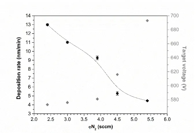
The target voltage (Vd) as well as the deposition rate (Rd) evolutions are plotted as a function of φN2 on Erreur ! Source du renvoi introuvable.. As expected, because of the poisoning, Rd continuously decreases when increasing φN2. This is explained either by the formation of an oxinitride compound at the surface of the target and/or by the increased φN2 ratio in the discharge associated with a decrease of Ar flow. On the other hand, Vd is roughly stable until φN2 = 3.9 sccm and dramatically increases at higher φN2. This value of φN2 therefore corresponds to the critical φN2 for which the poisoning occurs.
3.2. Chemical and crystalline properties of the films
Ti2p core level spectra were acquired for all samples after transfer to the XPS machine and sputtering with an Ar+ gun. The spectra were fitted by Gaussian functions and decomposed in three doublets: (i) 463.9 and 458.2 eV, (ii) 460.5 and 454.5 eV and (iii) 461.4 and 455.6 eV (see Erreur ! Source du renvoi introuvable.a). The binding energies and the splitting of 5.7 V of the first doublet matches with Ti4+ (1/2) and (3/2) in TiO2 [27,28]. The second doublet is much more difficult to attribute since it can correspond to: (i) Ti3+ in bulk TiN [29], (ii) Ti3+ associated to O vacancies in TiO2 lattice [28], or (iii) Ti2+ state for which TiO and TiN species contribute [30]. However, the peak splitting of 6 eV and the position of the 2p3/2 contribution are in favor of the presence of TiN [27]. Therefore, the third doublet is finally attributed to an intermediate specie which could be an oxynitride compound [29].
The peak area of each doublet is then evaluated for all samples and plotted as a function of φN2 (see Erreur ! Source du renvoi introuvable.b). Whatever the φN2 value, the film composition is dominated by TiO2 (doublet 1) which tends to suddenly decreases for φN2 ~ 3.9
sccm and then stabilizes again. The reverse evolution is observed for the doublet 2 supposedly related to TiN. This observation is correlated to the Vd evolution: if N is preferentially bounded to Ti in the material for φN2 > 3.9 sccm, Ti could also be preferentially linked to N at the surface of the target while a competition between O and N bonding takes place when φN2 < 3.9 sccm. Finally, we observed that doublet 3, related to the intermediate phase, presents the same contribution in the entire φN2 range.
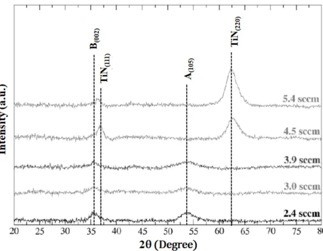
Erreur ! Source du renvoi introuvable., reporting the evolution of the crystalline constitution of the films as a function of φN2, shows that a transition between a brookite-anatase TiO2 mixture to TiN occurs for φN2 > 3.9 sccm which is in line with the evolution of the film chemistry and therefore support our XPS peak attribution.
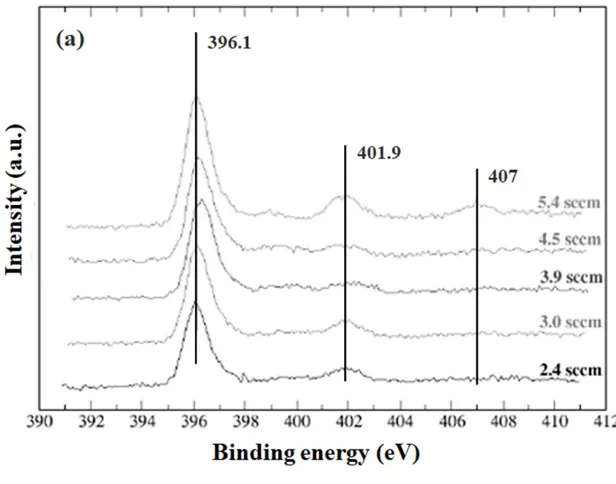
N1s core level XPS spectra are easier to analyze since they mainly exhibit two peaks for all φN2 values excepted for the highest N2 flow (φN2 = 5.4 sccm) for which an additional peak is observed at 407 eV (see Erreur ! Source du renvoi introuvable.a). The peak at 396 eV is well known and is characteristic to the Ti-N bond in N-Ti-N or O-Ti-N structures [11,27,29]. Nevertheless, even if it is not possible to discriminate this two compounds, this peak unambiguously indicates the presence of substitutional N atoms (NS) in our material. The two other contributions at 401.9 and 407.0 eV are attributed to N=O and NO2 species, respectively, and are therefore characteristic to interstitial N atoms (Ni) [11,27,29]. The shape of the O1s (see Erreur ! Source du renvoi introuvable.b) spectra is composed by a main peak between 530.0 and 530.6 eV characteristic to Ti-O-Ti with a shoulder between 531.5 and 532.0 likely associated with the oxynitride form [31,32].
Erreur ! Source du renvoi introuvable. reveals the evolution of the chemical composition of the film (empty symbols) as a function of φN2 as well as, the evolution of both substitutional and interstitial nitrogen atoms based on the previously described analysis of the N1s peak. These results show that whatever φN2, the Ni at.% remains relatively low and that
most of the N atoms are substitutional. This is in line with the results of Erreur ! Source du renvoi introuvable.b, i.e. the important proportion of N-Ti-N and N-Ti-O species (doublet 2 and doublet 3, respectively) in the films whatever φN2. Moreover, it also appears that Ntot and thus %Ns can be almost linearly controlled from 7 to 12% by tuning φN2. The increase of %Ntot with φN2 is associated with the decrease of O at.% since Ti at.% remains stable. Based on these results, it seems that for 0 < φN2 < 3.9 sccm, O atoms are progressively replaced by N atoms in the material when increasing φN2. For φN2 > 3.9 sccm, the amount of O2 provided to the discharge becomes too low and the formation of N-Ti-N is favored to the detriment of TiO2 as suggested by Wong et al. [31]. These observations are also in agreement with the evolution of Vd.
3.3. Optical and electrical properties
The optical and electrical properties of the films grown for φN2 = 2.4, 3.9, 4.5 and 5.4 sccm are summarized in Erreur ! Source du renvoi introuvable.. They were compared to pure TiO2 thin films grown in the similar conditions which exhibit a high transmission of 75.4% in the visible range, a wide optical bandgap of 3.16 eV, a n-type conductivity and an electron density ~ 1010 cm-3. Nevertheless, it has to be mentioned that the electrical properties of this films were extremely tricky to evaluate due to the high resistivity of the material which is the cause of the low solar-to-electricity conversion efficiency of the DSSCs based on this material, as mentioned in the introduction.
The N doping allows to modify the semiconducting behavior since samples 1 to 4 exhibit a positive Hall coefficient indicating a p-type conductivity. The hall coefficient of samples 3 and 4 (prepared using the highest φN2 values and which is close to 0) is considerably lower than the ones of the samples 1 and 2. This could traduce the difficulty to identify the main carrier because the electronic behavior of these films is more likely close to the one of a metal than to a semiconductor material. This can also explain the drop of conductivity between
the two groups of samples from 10−3 to 10−1 Ω−1.cm−1, and the high carrier concentration of samples 3 and 4 (~ 1018 cm−3). Altogether these electrical properties are consistent with the pronounced TiN character of these films. Obviously, these are not suitable to be used as photocathode in a p-DSSC because they would induce short-circuit in the cell.
On the other hand, films 1 and 2 (prepared using the lowest φN2 values) characterized by a lower concentration of dopant present proper electrical properties for DSSCs applications that are in line with ALD synthesized N-doped TiO2 [20]. Another remarks concern the measured hole mobility which is clearly enhanced compared to previously reported values for sputtered NiO (< 0.5 cm2.V−1.s−1) and a quite similar conductivity which could be due to a lower concentration of defects. However, the hole concentration is lower than the one generally obtained with NiO, i.e. ~ 1017 – 1019 holes/cm³ [33,34].
In order to complete these electrical characterizations, Mott-Schottky measurements were performed on sample 1. This technique allows to simulate the semi-conductor/electrolyte interface by an equivalent electrical circuit (EEC). The obtained Nyquist diagram is characterized by two loops. As a consequence, two capacities can be extracted: C2 is associated to the first loop (at high frequencies) and is correlated with the bulk properties of the material while C3 is associated with the second loop (at low frequencies) and reveals the interface properties. The results are presented on Erreur ! Source du renvoi introuvable..
First, the positive slope of both patterns indicates that TiO2:N is characterized by a p-type behavior which is in agreement with the Hall effect measurements. The hole density can be extracted for both interface and bulk components. Indeed, the slope of the linear part, corresponding to the depletion state, is equal to the term before the brackets of relation (1). This lead to a hole density of ~ 8.1015 holes/cm² at the surface and ~ 6.1017 holes/cm² in the depth of the film. To explain this difference, a XPS profile was performed (see Erreur ! Source du renvoi introuvable.) and revealed that the N at.% is 3% higher in the bulk of the material
because of a surface oxidation which may occurred during the transport of the sample to the XPS chamber.
The flat-band potential (Vfb), which gives an idea of the maximum Voc that could be delivered by the cell, can be estimated as the intersection between the X-axe and the extrapolation of the linear part. It varies between 0.32 V at the surface and 0.36 V in the bulk which is higher than the one of NiO, i.e. 0.27 V, also measured for this work, meaning that the synthesized TiO2:N exhibit interesting electrical properties to replace NiO as hole transport layer in p-DSSCs. The lower Vfb at the surface of the material could be explain by the lowest doping.
If the electrical properties of our material are obviously promising, it has to be mentioned that the optical properties of the films can be a limitation. Indeed, samples 1 and 2 exhibit a lower optical transmission compared to sputtered NiO, e.g. ~ 55% [33,34]. It is clear that the optical transmission falls as the dopant concentration increases due to a narrowing and thus a red shift of the material optical bandgap, as explained in the introduction part. It could therefore be improved by carefully decreasing the dopant concentration to approach the transmittance of pure TiO2.
4. Conclusions
To conclude, we report for the first time the synthesis of p-type nitrogen-doped titanium oxide thin films by DC co-reactive magnetron sputtering. It is shown that by carefully tuning the ratio between O2 and N2 reactive gases, the amount and the type (substitutional vs interstitial) of N doping of TiO2 can be finely controlled. N atoms are consequently mainly incorporated at substitutional positions which leads to the synthesis of p-type thin films, as demonstrated by Hall effect and Mott-Schottky measurements. Even if some electrical and optical parameters of the films can be improved in comparison with previously NiO sputtered
films, i.e. hole density and optical transmission, we believe that this work opens the door for future development of tandem DSSCs fully based on TiO2 by using a single and already industrialized deposition system.
Acknowledgement
A. Panepinto thanks F.R.I.A grant of National Fund for scientific Research (FNRS – Belgium).
References
[1] B. O’Regan & M. Grätzel, Nature, 1991, 353, 737–740
[2] K. Kakiage, Y. Aoyama, T. Yano, K. Oya, J. Fujisawa & M. Hanaya, Chem. Commun., 2015, 51, 15894–15897
[3] J. Gong, J. Liang & K. Sumathy, Renew. Sustain. Energy Rev., 2012, 16, 5848–5860
[4] F. Odobel, L. Le Pleux, Y. Pellegrin & E. Blart, Acc. Chem. Res., 2010, 43, 1063–71
[5] Y. Farré, M. Raissi, A. Fihey, Y. Pellegrin, E. Blart, D. Jacquemin & F. Odobel,
ChemSusChem, 2017, 10, 2618–2625
[6] F. Odobel, Y. Pellegrin, E. a. Gibson, A. Hagfeldt, A. L. Smeigh & L. Hammarström,
Coord. Chem. Rev., 2012, 256, 2414–2423
[7] A. Nattestad, I. Perera & L. Spiccia, J. Photochem. Photobiol. C Photochem. Rev., 2016
[8] N. Marinakis, M. Willgert, E. C. Constable & C. E. Housecroft, Sustain. Energy Fuels, 2017, 1, 626–635
[9] J. Dervaux, P. -a. Cormier, S. Konstantinidis, R. Di Ciuccio, O. Coulembier, P. Dubois & R. Snyders, Vacuum, 2015, 114, 213–220
[10] V. C. Anitha, A. N. Banerjee, S. W. Joo & B. K. Min, J. Ind. Eng. Chem., 2015, 29, 227–237
[11] R. Asahi, T. Morikawa, H. Irie & T. Ohwaki, Chem. Rev., 2014, 114, 9824–9852
[12] C. Di Valentin & G. Pacchioni, Catal. Today, 2013, 206, 12–18
[13] S. Wang, L. Pan, J.-J. Song, W. Mi, J.-J. Zou, L. Wang & X. Zhang, J. Am. Chem. Soc., 2015, 137, 2975–2983
[14] S. Das, D. Liu, J. B. Park & Y.-B. Hahn, J. Alloys Compd., 2013, 553, 188–193
[15] M. V. Dozzi & E. Selli, J. Photochem. Photobiol. C Photochem. Rev., 2013, 14, 13–28
[16] D. A. Duarte, M. Massi & A. S. da Silva Sobrinho, Int. J. Photoenergy, 2014, 2014, 1– 13
[17] M. Batzill, E. H. Morales & U. Diebold, Phys. Rev. Lett., 2006, 96, 26103
[18] T. Lindgren, J. M. Mwabora, E. Avendaño, J. Jonsson, A. Hoel, C.-G. Granqvist & S.-E. Lindquist, J. Phys. Chem. B, 2003, 107, 5709–5716
[19] B. Liu, L. Wen & X. Zhao, Sol. Energy Mater. Sol. Cells, 2008, 92, 1–10
[20] K. Vasu, M. B. Sreedhara, J. Ghatak & C. N. R. Rao, ACS Appl. Mater. Interfaces, 2016,
8, 7897–7901
[21] R. Snyders, R. Gouttebaron, J. P. Dauchot & M. Hecq, J. Anal. At. Spectrom., 2003, 18, 618
[22] O. Diwald, T. L. Thompson, E. G. Goralski, S. D. Walck & J. T. Yates, J. Phys. Chem.
[23] D. Thiry, F. J. Aparicio, P. Laha, H. Terryn & R. Snyders, J. Vac. Sci. Technol. A
Vacuum, Surfaces, Film., 2014, 32, 50602
[24] J. Tauc, R. Grigorovici & A. Vancu, Phys. Status Solidi
[25] G. L. Humphrey, J. Am. Chem. Soc., 1951, 73, 1587–1590
[26] G. L. Humphrey, J. Am. Chem. Soc., 1951, 73, 2261–2263
[27] E. Martínez-Ferrero, Y. Sakatani, C. Boissière, D. Grosso, A. Fuertes, J. Fraxedas & C. Sanchez, Adv. Funct. Mater., 2007, 17, 3348–3354
[28] a. Nambu, J. Graciani, J. a. Rodriguez, Q. Wu, E. Fujita & J. F. Sanz, J. Chem. Phys., , DOI:10.1063/1.2345062
[29] N. C. Saha & H. G. Tompkins, J. Appl. Phys., 1992, 72, 3072–3079
[30] V. Stranak, M. Quaas, R. Bogdanowicz, H. Steffen, H. Wulff, Z. Hubicka, M. Tichy & R. Hippler, J. Phys. D. Appl. Phys., 2010, 43, 285203
[31] M.-S. Wong, H. Pang Chou & T.-S. Yang, Thin Solid Films, 2006, 494, 244–249
[32] A. Trenczek-Zajac, M. Radecka, K. Zakrzewska, A. Brudnik, E. Kusior, S. Bourgeois, M. C. M. de Lucas & L. Imhoff, J. Power Sources, 2009, 194, 93–103
[33] H.-L. Chen, Y.-M. Lu & W.-S. Hwang, Surf. Coatings Technol., 2005, 198, 138–142
[34] H. Sato, T. Minami, S. Takata & T. Yamada, Thin Solid Films, 1993, 236, 27–31
Figures captions
Fig. 1: Evolution of the deposition rate and the target voltage as a function of φN2. φO2 is fixed
at 1.2 sccm.
Fig. 2: Ti2p core level spectra (a) and peak area evolution of the three Ti doublets (b) for films
Fig. 3: GIXRD spectra of the films with φO2 = 1.8 sccm and φN2 varying from 2.4 to 5.4 sccm.
Fig. 4: N1s core level (a) and O1s core level (b) spectra of the films synthesized with φO2 =
1.8 sccm and φN2 varying from 2.4 to 5.4 sccm.
Fig. 5: Atomic relative concentrations of the films synthesized with φO2 = 1.8 sccm and φN2
varying from 2.4 to 5.4 sccm.
Fig. 6: Mott-Schottky plots of sample 1 related to the (a) interface behaviour and (b)bulk
behaviour.
Fig. 7: Nitrogen and oxygen XPS depth profile analysis of sample 1.
Table1: Electrical and optical properties of TiO2:N films synthesized with φO2 = 1.8 sccm and
φN2 varying from 2.4 to 5.4 sccm.
Fig. 2: Ti2p core level spectra (a) and peak area evolution of the three Ti doublets (b) for films synthesized with φO2 = 1.8
Fig. 4: N1s core level (a) and O1s core level (b) spectra of the films synthesized with φO2 = 1.8 sccm and φN2 varying from
Fig. 5: Atomic relative concentrations of the films synthesized with φO2 = 1.8 sccm and φN2 varying from 2.4 to 5.4 sccm.
Fig. 7: Nitrogen and oxygen XPS depth profile analysis of sample 1.
Table 1:Electrical and optical properties of TiO2:N films synthesized with φO2 = 1.8 sccm and φN2 varying from 2.4 to 5.4
sccm. Sample φN2 (sccm) [N] (%) Transmittance (%) Optical gap (eV) Hall Coefficient (cm³.C-1) Carrier density (cm-3) Conductivity (Ω-1.cm-1) Mobility (cm².V-1.s) NiO [33] 1 2 3 4 / 2.4 3.9 4.5 5.4 / 7.55 8.40 10.44 11.55 ~ 55 45.13 36.54 8.43 3.96 / 2.24 2.07 2 1.95 ~ 120 1397 1231.4 3.26 0.64 ~ 1017-19 5.22 1015 1.32 1016 5.31 1018 9.00 1018 ~ 2.00 10-3 4.08 10-3 2.51 10-3 5.24 10-1 2.67 10-1 < 0.5 1.5 3.1 1.71 0.88