HAL Id: hal-02307102
https://hal.archives-ouvertes.fr/hal-02307102
Submitted on 7 Oct 2019
HAL is a multi-disciplinary open access
archive for the deposit and dissemination of
sci-entific research documents, whether they are
pub-lished or not. The documents may come from
teaching and research institutions in France or
abroad, or from public or private research centers.
L’archive ouverte pluridisciplinaire HAL, est
destinée au dépôt et à la diffusion de documents
scientifiques de niveau recherche, publiés ou non,
émanant des établissements d’enseignement et de
recherche français ou étrangers, des laboratoires
publics ou privés.
Modelling of a 3D Periodic Surface Based on a Folded
Resonator Embedded into a Waveguide
Paul Le Bihan, Maria Garcia-Vigueras, Erwan Fourn, Raphaël Gillard,
Isabelle Le Roy Naneix, Stefan Varault, Christian Renard
To cite this version:
Paul Le Bihan, Maria Garcia-Vigueras, Erwan Fourn, Raphaël Gillard, Isabelle Le Roy Naneix, et al..
Modelling of a 3D Periodic Surface Based on a Folded Resonator Embedded into a Waveguide. 49th
European Microwave Conference, Oct 2019, Paris, France. �hal-02307102�
Modelling of a 3D Periodic Surface Based on a
Folded Resonator Embedded into a Waveguide
Paul Le Bihan
#1, María García-Vigueras
#2, Erwan Fourn
#, Raphaël Gillard
#, Isabelle Le Roy Naneix
*3, Stefan Varault
*,
Christian Renard
*#Univ Rennes, INSA Rennes, IETR, UMR CNRS 6164, F-35000 Rennes, France *THALES Defense Missions Systems, Elancourt, France
{1paul.le-bihan, 2maria.garcia-vigueras}@insa-rennes.fr, 3[email protected]
Abstract — This paper presents the analysis and modelling of
a specific type of three-dimensional frequency-selective surface which unit cells are named as Waveguide Integrated Resonators. This unit cell is identified as a promising structure for broadband filtering applications. An original circuital approach is adopted in order to model this complex volume structure. An equivalent circuit is proposed which reproduces the structure’s behaviour under normal incidence. Very good accuracy is obtained within the frequency band of interest, thus validating the proposal.
Keywords — frequency selective surfaces, periodic structures,
equivalent circuits.
I. INTRODUCTION
A Frequency Selective Surface, also called FSS, is an assembly of cells periodically placed to build a 2D array [1]. When an electromagnetic plane wave hits the FSS, only a part of the energy is transmitted to the other side of the surface, thus acting as a filter. Its response with frequency, polarization and incidence angle depends on the geometry of the unit cell, but also its periodicity and the materials it is made of. FSS usually find their application in radomes, reflectors or absorbing structures [2-3].
Traditionally composed of metallic elements printed on dielectric substrate slabs, FSS can be stacked into multilayer structures to reach higher order frequency responses. Considerable efforts have been put into the analysis of these surfaces, ending up with equivalent models describing their behaviour, such as in [4]. Nowadays, the required performances of these technologies are more and more challenging. Large bandwidth, high selectivity, dual-polarisation operation and oblique incidence independence are main criteria of choice.
The rise of new 3D printing techniques, also called additive manufacturing, allows developing more and more complex structures. As a consequence, new types of frequency selective structures emerge from the literature, made from not just planar, but also three-dimensional elements, like [5-6]. These so-called 3DFSS may provide new solutions to reach better filtering performance. As the interaction between plane waves and these 3D structures is often difficult to handle, there is a strong need for equivalent models that allow not only to understand how they work, but also to facilitate the design, limiting the need for commercial solvers. The present contribution concentrates on the unit cell recently proposed in [7-9]. A unit cell consisting
on Waveguide Integrated Resonator (WIR) is there considered, which presents interesting filtering properties, such as a wide bandpass and high rejection levels. While this structure was already introduced in literature, a modeling approach describing its behaviour has not been presented so far, and this is what this paper aims at. Our study focuses on the analysis of the unit cell under normal incidence and leads to a simple equivalent circuit, which shows great benefit in the design process.
The paper is organized as follows. First of all, the structure and its global modelling approach are presented. The unit cell is then split into two sub-elements which are studied separately. From these distinct studies, the complete equivalent model of the WIR is defined. At last, a parametric study is led to validate the reliability of the proposed circuit.
II. WIR CIRCUIT MODELLING
Among 3DFSS, the WIR outstands for its wide bandwidth (67%) and high rejection levels. Past works presented in [7-9] focus on the structure presented in Fig. 1(a). This unit cell is composed of a square metallic waveguide loaded with four folded wire resonators. Two of them (blue in Fig. 1) are sensitive to vertically polarized incident waves due to their y-oriented terminal sections while the two remaining ones (in red) are sensitive to horizontal polarization. For the sake of simplicity, our study focuses on the simplified structure presented in Fig. 1(b) with only the V-polarized resonators.
(a) (b)
Fig. 1. WIR unit cell: (a) Dual-pol. structure; (b) Single-pol. Structure (lz = 7.5
mm; ly = 3.75 mm; gap = 0.3 mm; t = 7 mm; D = 9 mm. Waveguide’s walls
and wires’ diameter : 0.1 mm)
In order to characterize such a complex 3D structure, an equivalent circuit is of great interest. As a preliminary step, Fig. 2 illustrates the transmission mechanism through the cell.
Fig. 2. Model of the WIR structure.
The proposed model is composed of two parallel paths connecting the input port (port 1, at the front) to the output port (port 2, at the rear). Indeed, the input power can be transferred to the output, either through the waveguide itself (upper path), or the resonators (lower path). More precisely, a fraction of the incident power is coupled to the y-oriented arms of the resonators at the input port. It is converted to electric currents along the wires before being radiated by the y-oriented arms at the output port. The residual fraction of the incident power can be transmitted through the waveguide, or simply reflected back.
III. WIREQUIVALENT CIRCUIT
On a first approach, the analysis of the entire structure is very complex to handle. The choice has been made to separate the unit cell into two sub-elements, i.e. the square waveguide and the folded resonator. They have been studied separately in order to easily identify their own contribution to the global response of the 3DFSS under normal incidence.
A. Resonator modelling
The first step consists in modelling the behaviour of the resonator separated from the waveguide. This results in the equivalent model presented in Fig. 3.
Fig. 3. Folded resonator equivalent model.
As in Fig.1, this model is composed of two branches in parallel connecting ports 1 and 2. The lower branch stands for the power coupled to the resonator. The upper branch stands for the free space transmission. It replaces the propagation in the waveguide observed in the upper branch of Fig. 2. Transformers T1 and T2 represent the coupling between the incident wave and the vertical wires of the resonator. The lower branch is split into three transmission lines representing the different sections of the wire. Currents on the vertical sections are supported by a transmission line of length ly, free-space impedance (η0), and wave number (k0). For the longitudinal section of the resonator, a bifilar line model is used to account for the coupling between
the two close horizontal wires. The impedance of this line is given by 𝑍𝑙𝑖𝑛𝑒=
𝜂0
𝜋acosh ( 𝑔𝑎𝑝
𝑡ℎ𝑘) , where thk stands for the diameter of the metallic wires. A reduction factor r is also applied to the overall length of the wire, accounting for the effect of the right angle bends.
In order to determine the coefficients T1, T2 and r, one full wave simulation is needed to compute the frequency response of the structure. This simulation of the unit cell is realized in a periodic boundary environment of periodicity D thanks to the commercial software CST Microwave Studio. Then, an optimization of the equivalent circuit is realized to retrieve values of these coefficients which permit to fit the full wave response at best on a large frequency band.
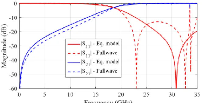
Fig. 4 shows the S-parameters response of the folded resonator obtained from CST Microwave Studio, compared to the equivalent circuit results. Our work focuses on the region below the onset of higher Floquet modes, which happens at 33.3 GHz, according to the value of the unit cell’s periodicity D. The frequency response of the resonator is characterized by successive transmission zeroes. These resonances appear when the total length of the folded wires equals a multiple of half a wavelength. A maximum amount of coupling is then reached. Results show that the equivalent circuit in Fig.3 allows a very good accuracy regarding the position of the transmission poles and zeros of the folded resonator’s S-parameters response. Transmission levels are also globally well predicted.
Fig. 4. Folded resonator S-parameters: equivalent model to full wave analysis comparison.
B. Waveguide modelling
The second step of our study aims at modelling the waveguide section. It can be represented by a dispersive transmission line loaded with shunt admittances (Ydisc) accounting for the discontinuities at input and output, as depicted in Fig. 5.
Fig. 5. Equivalent model of the waveguide under normal incidence.
Propagation only involves the fundamental TE10 mode of
the waveguide (with propagation constant β10 and modal impedance ZTE10) since the cut-off frequency of its first higher
mode compatible with excitation and structure’s symmetry is out of the band considered in our study.
The admittance’s value is determined using a fitting study analogue to the one used for the resonator study. More precisely, Ydisc is optimized so that the analytically-calculated S-parameters for the equivalent circuit in Fig. 5 match those
given by a full wave simulation of the waveguide. Results using this retrieving method are presented in Fig. 6. A very good agreement is observed, especially for S21. As frequency
increases, accuracy deteriorates (mainly regarding the positions of S11 minima). This can be explained by the quite approximate
model we use for Ydisc, i.e. a simple shunt LC resonator with quasi-static capacitive and inductive elements. However, the obtained agreement is sufficient for our purpose.
Fig. 6. Waveguide S-parameters: equivalent model to full wave analysis comparison.
C. WIR complete model
The global frequency response of the complete structure can be seen as a combination of the characteristics of each of its sub-element, each of them offering a path for the energy to be transmitted. However, it is not a simple superposition of these responses.
As we have seen with the resonator alone (section III.A), two propagation paths are involved: one through the metallic wires, and another one through the free space between the y-directed arms of the structure. In order to take into account the effect of the waveguide, we now replace this free-space propagation by propagation through a dispersive line with impedance ZTE10 and phase constant βTE10, as described in Fig. 5. On the other hand, we also consider that the waveguide does not modify the propagation along the resonator’s wires. At each end of the dispersive line, Ydisc admittances account for the air-to-waveguide discontinuity, mentioned in Section III.B. This approach leads to the electrical equivalent circuit presented in Fig. 7. It is also important to mention that, in this equivalent circuit, distance between the vertical arms and the waveguide openings are taken into account by transmission lines of length 𝑙𝑧−𝑡
2 . S-parameter results of this circuit are shown in Fig. 8.
Fig. 7. Equivalent circuit of the WIR structure under normal incidence.
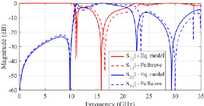
Fig. 8. WIR structure S-parameters under normal incidence: equivalent model to full wave analysis comparison.
As can be seen in Fig. 8, the WIR exhibits a wide transmission bandwidth characteristic between 10.6 GHz and 22.6 GHz. Mismatching rise can be observed around 12 GHz, but it can be reduced by adjusting dimensions of the structure, thus moving up the first transmission pole. Multiple resonances of the resonator provide transmission zeroes which offer a good rejection. Here again, high band rejection level can be improved by optimizing structure’s dimensions. Low band rejection is obtained from the evanescent behaviour of the waveguide, which finds its cutoff at 17 GHz. The equivalent model of Fig. 5 reproduces with a good accuracy the structure’s behaviour on the overall bandwidth of study. Yet, the frequency response is slightly shifted, despite a very good tuning of each parameter of the sub-elements studied separately. The main hypothesis of this shift is that it is produced by couplings between the resonator and the waveguide which are not taken into account into this simple equivalent circuit. However, despite of these deviations, WIR behaviour is well predicted, with the apparition of transmission zeros in the high frequency rejection bandwidth. The developed equivalent circuit is then a reliable model, which can be used in a design process of such structure, before a final full wave optimisation.
D. Circuit parametric evaluation
The final step of this study is to validate through parametric studies how the equivalent model can follow frequency tendencies of the structure’s response. In Fig. 8, frequency shifts can be observed on the overall response of the model. Before realizing this parametric study, it has been decided to re-fit coefficients T1, T2 and r of the circuit. Result of this optimization is shown Fig. 9.
Fig. 9. WIR structure S-parameters under normal incidence: equivalent model to full wave analysis comparison after re-optimization of T1, T2 and r.
Once this tuning has been realized, variation of the bandwidth with geometrical parameters is analysed observing the position of the first transmission pole and the second transmission zero, initially at 10.8 GHz and 23.5 GHz, respectively. Both are directly linked to the resonant frequencies of the folded wires. As seen in Fig. 10, the equivalent circuit follows very well this variation versus lengths
ly and lz. Fig. 11 shows that the bifilar line model allows reproducing quite well the evolution of the frequency response as a function of wires’ thickness and the gap between resonators in the case of the first transmission pole. Yet, in the case of the second transmission zero, this model is not sufficient anymore to predict the shifts. Further investigations are necessary to conclude on this point and improve the circuit’s predictions.
(a) (b)
Fig. 10. Variation of the first transmission pole and second transmission zero with wires lengths.
(a) (b)
Fig. 11. Variation of the first transmission pole and second transmission zero with the gap between the resonators and the wires’ thickness.
IV. CONCLUSION
The analysis and modelling by an electrical equivalent circuit of a three-dimensional frequency selective structure has been presented in this paper. This model describes with a good accuracy the transmission and reflection properties of the Waveguide Integrated Resonator (WIR) illuminated by a normal incidence plane wave. Parametric studies have shown that this model is able to reproduce effects of geometric variations of the 3DFSS, proving that it can be used as a useful tool in a design process.
REFERENCES
[1] B. Munk, Frequency Selective Surfaces: theory and design, Wiley, 2001. [2] P. Mahima, S. Sangeetha et al, “EM Design of Hybrid-element FSS Structure for Radome Application”, 2016 IEEE Annual India
Conference (INDICON).
[3] José Jaime Guimarães Peixoto Neto, Antonio Luiz P. de S. Campos, “Proposal of a Microwave Absorber Using FSS with Square Loops”,
2017 SBMO/IEEE MTT-S International Microwave and Optoelectronics Conference (IMOC).
[4] M. A. Al-Joumayly, N. Behdad, “A generalized method for synthesizing low-profile, band-pass frequency selective surfaces with non-resonant constituting elements”, IEEE Transactions on Antennas and
Propagation, Volume 58, Issue 12, Dec. 2010.
[5] J. Zhu, W. Tang et al, “Dual-Polarized Bandpass Frequency-Selective Surface With Quasi-Elliptic Response Based on Square Coaxial Waveguide”, IEEE Transactions on Antennas and Propagation, Volume 66, Issue 3, March 2018.
[6] B. Li, Z. Shen, “Three-Dimensional Dual-Polarized Frequency Selective Structure With Wide Out-of-Band Rejection”, IEEE Transactions on
Antennas and Propagation, Volume 62, Issue 1, Jan. 2014
[7] R. Mittra, C. Pelletti, “Three-dimensional FSS Elements with Wide frequency and Angular Responses”, Proceedings of the 2012 IEEE
International Symposium on Antennas and Propagation.
[8] C. Pelletti, R. Mittra, et al, “Three dimensional FSS Elements with Wide frequency and angular response”, Proceedings of 2013 URSI
International Symposium on Electromagnetic Theory (EMTS).
[9] C. Pelletti, G. Bianconi, et al, “Frequency Selective Surface with wideband quasielliptic bandpass response”, Electronics Letters, Volume 49, Issue 17, August 15 2013.