HAL Id: hal-00003590
https://hal.archives-ouvertes.fr/hal-00003590
Submitted on 15 Dec 2004
HAL is a multi-disciplinary open access
archive for the deposit and dissemination of
sci-entific research documents, whether they are
pub-lished or not. The documents may come from
teaching and research institutions in France or
abroad, or from public or private research centers.
L’archive ouverte pluridisciplinaire HAL, est
destinée au dépôt et à la diffusion de documents
scientifiques de niveau recherche, publiés ou non,
émanant des établissements d’enseignement et de
recherche français ou étrangers, des laboratoires
publics ou privés.
Resonant Raman scattering in GaAsN: Mixing,
localization and band impurity formation of electronic
states
Guillaume Bachelier, Adnen Mlayah, M. Cazayous, Jesse Groenen, Antoine
Zwick, Hélène Carrère, Eléna Bedel-Pereira, Alexandre Arnoult, A. Rocher,
Anne Ponchet
To cite this version:
Guillaume Bachelier, Adnen Mlayah, M. Cazayous, Jesse Groenen, Antoine Zwick, et al.. Resonant
Raman scattering in GaAsN: Mixing, localization and band impurity formation of electronic states.
Physical Review B: Condensed Matter and Materials Physics (1998-2015), American Physical Society,
2003, 67, pp.205325. �hal-00003590�
formation of electronic states
G. Bachelier, A. Mlayah, M. Cazayous, J. Groenen, and A. Zwick
Laboratoire de Physique des Solides UMR 5477, IRSAMC,
Universit´e P. Sabatier, 118 route de Narbonne, 31062 Toulouse Cedex 4, France
H. Carr`ere, E. Bedel, and A. Arnoult
Laboratoire d’Architecture et d’Analyse des Syst`emes UPR 8001, 7 Av. Du Colonel Roche 31077 Toulouse, France
A. Rocher and A. Ponchet
Centre d’Elaboration de Mat´eriaux et d’Etudes Structurales UPR 8011, 29 rue Jeanne Marvig, 31400 Toulouse, France
Raman measurements on a thick GaAsN layer and on GaAsN/GaAs quantum well structures are reported. The scattering was excited close to resonance with the N-induced E+ transition,
and detected in both Stokes and anti-Stokes regions including the low-frequency range around the Rayleigh line. A broad continuous scattering due to acoustic phonons is observed on the thick GaAsN layer. Calculations of the Raman efficiency showed that localization and mixing of the resonant electronic states well account for the measured spectral lineshapes. The localization length around a single nitrogen impurity is estimated and the band impurity formation discussed. Periodic oscillations of the scattered intensity are clearly observed on the quantum well structures. They are analyzed in terms of Raman interference effects due to spatial coherence of the resonant electronic states. We found that layering of the electronic density along the growth axis well accounts for the observed oscillations period, spectral envelope and interference contrast. The experimental data and the calculations support the formation of an impurity band.
PACS numbers: 78.30.-j, 63.20.Kr, 81.07.Ta, 81.15.Hi
I. INTRODUCTION
The substitution of only 1% As atoms by N atoms in GaAs has important impacts on the electronic and
opti-cal properties such as giant band gap bowing,1–3unusual
pressure dependence of the band gap4,5 and large
effec-tive masses.6,7 Two models were proposed for the
elec-tronic structures of ternary alloys of highly mismatched
binary semiconductors (e.g. GaN/GaP, GaN/GaAs,
GaN/InAs). One is the band anti-crossing model (BAC),
proposed by Shan et al.,4,8,9in which the electronic state
of the isovalent impurity interacts strongly with the low-est conduction band states of the host material. The energies of the coupled electronic subbands, calculated using the BAC model, are in good agreement with the
spectral features labelled E− and E+ revealed by
photo-reflectance (PR)3,4 and photo-luminescence (PL)5
mea-surements; the coupling strength was however used as an adjustable parameter. The BAC model is a phenomeno-logical model since neither the origin of coupling nor the localization of the electronic states were considered
ex-plicitly. On the other hand Bellaiche et al.,10 Mattila et
al.11 and Kent et al.12,13 reported calculations of the
GaAsN and GaPN electronic structure using a pseudo-potential supercell technique. The composition and pres-sure dependence of the lowest conduction band states
were studied theoretically. It was shown that E− and
E+ are due to transitions from the valence band
max-imum (VBM) to conduction states involving a strongly
localized nitrogen state a1(N) mixed with host crystal
states a1(Γ), a1(L) and a1(X) arising from the Γ, L and
X valleys of the Brillouin zone. This approach well
ac-counts for the PL and PR data as the BAC model. But in addition to the transition energies, mixing and local-ization of the electronic states come out as results of the
calculations.11–13
The aim of this work is to show that mixing and local-ization can be addressed directly using resonant Raman scattering by acoustic phonons. Indeed, THz acoustic phonons revealed by Raman scattering have been suc-cessfully used as probes of the electronic wavefunction
localization and correlation in quantum wells14–16 and
quantum dots nanostructures17,18 . In these systems,
quantum confinement and artificial, as well as sponta-neous, ordering are responsible for the spatial localiza-tion and coherence of the electronic density. In GaAsN, the localization of the electronic density around the ni-trogen impurity originates in the large difference between the covalent radius of N (0.075 nm) and As (0.125 nm).
In this work we estimate the localization length and de-gree of mixing of the resonantly excited electronic states using Raman scattering by acoustic phonons. The results
2 are compared to calculations performed using the
pseudo-potential super-cell approach11–13and the large scale
lo-cal density approximation.19 Moreover, the band
impu-rity formation is adressed using interference Raman ef-fects generated in GaAsN/GaAs multilayers. It is worth-mentioning that, among the published Raman works on
GaAsN,20–29only few were devoted to acoustic phonons
scattering.22,29In addition only thick GaAsN layers were
studied up to now. Interference Raman effects similar
to those already observed on QD layers17,18 are here
re-ported for the GaAsN/GaAs quantum well structures.
II. EXPERIMENTS
A 1 µm thick GaAsN layer and three GaAsN/GaAs quantum well structures were grown by molecular beam epitaxy (MBE) on (100) GaAs. The MBE chamber is equipped with a HD25R Oxford RF plasma cell, which
provides reactive N species. Ultra-pure N2was obtained
from 6N nitrogen flowing through a heating getter
fil-ter to remove O2, H2O, CO, CO2 and other impurities.
The growth temperatures were 580◦C and 470◦C for the
GaAs buffer layer and for the GaAsN layer, respectively. Additional details of the growth conditions can be found
elsewhere.30
The nitrogen concentration was determined using sec-ondary ion mass spectroscopy (SIMS); a GaAsN layer previously characterized by X-Ray diffraction was used
as a reference. Cs+primary ions and CsM+ positive
sec-ondary ions configuration was used in order to provide a quantitative analysis of nitrogen content up to few per-cents.
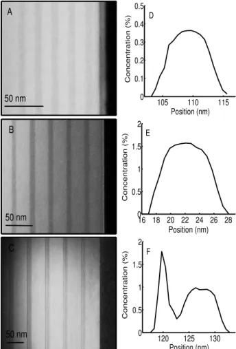
Figure 1 shows transmission electron microscopy
(TEM) image of the quantum well structures. Each
structure consists of five GaAsN layers separated by GaAs spacers. The thickness of the GaAsN layers is around 9 nm for all structures whereas the barrier thick-ness is 12 nm, 24 nm or 39 nm. The GaAs top layer has the same thickness as the GaAs barriers.
For each structure the incorporation profiles of the ni-trogen, along the growth direction and in the plane of the GaAsN layers, were measured using a quantitative analysis of the TEM image contrast. Typical profiles are shown in Fig. 1. For samples A and B, the nitrogen distri-bution inside the quantum wells is rather homogeneous. Whereas, for sample C, it is clearly non uniform. This is due to different growth conditions: the GaAs, grown before the GaAsN layers, once the plasma was ignited and the shutters still closed, was 4 nm thick for sample C and 1 nm for samples A and B, explaining why the GaAsN layers are thicker for this sample. Moreover, the plasma ignition duration may have been longer than for the other samples. Also, a lower substrate temperature (during the plasma ignition) may enhance the nitrogen deposition on the surface.
The Raman measurements were performed at liquid nitrogen temperature. The scattering was excited using
50 nm A 105 110 115 0 0.1 0.2 0.3 0.4 0.5 Concentration (%) taille du puits: 8.0986nm
cmoyen~0.4368% taille du puits: 8.0986nmcmoyen~0.53779% taille du puits: 8.0986nmcmoyen~0.44805% cmoyen~0.42569%
Position (nm) D 50 nm B 16 18 20 22 24 26 28 0 0.5 1 1.5 2 Concentration (%) Position (nm) E 50 nm C 120 125 130 0 0.5 1 1.5 2 Concentration (%) Position (nm) F
FIG. 1: TEM images of samples A, B and C. The nitrogen in-corporation profiles along the growth direction were obtained by a quantitative analysis of the TEM image contrast (spectra D, E and F).
the red and yellow lines of a Kr laser. The scattered light was dispersed using a triple T800 Coderg spectrometer and detected with a single channel GaAs photo-cathode.
III. RESULTS AND DISCUSSION
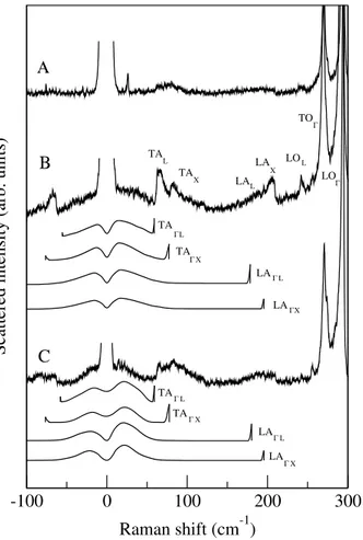
Figure 2 presents Stokes and anti-Stokes Raman
spec-tra from the thick GaAs1−xNxlayer with xSI M S = 0.8%.
First and second order scattering by zone center
trans-verse TOΓand longitudinal LOΓoptical phonons of GaAs
are observed. Scattering by the local vibrational mode (LVM) of isolated GaN bonds is also visible around
470 cm−1. The dependence of the frequency and
inten-sity of the TOΓ, LOΓ and LVM lines, on the nitrogen
concentration, has been already studied in Refs. 21,23,25.
In particular, Prokofyeva et al.21 and Wagner et al.23
showed that calibration of the frequency shift of the LOΓ
and LVM lines gives a reliable, rapid and non destructive method for determining the nitrogen content. Using the
linear variations, as proposed by Prokofyeva et al.,21and
-100
0
100
200
300
Raman shift (cm
-1)
Scattered intensity (arb. units)
TA TA Γ Γ L TA X TA L X LA Γ Γ LA LA LA Γ Γ Γ Γ L L X X TOΓ LOL LA X LAL TAX TAL LOΓ
Α
Β
C
FIG. 2: Resonant Raman spectra from the 1 µm thick GaAs1−xNx layer for excitation at 1.83 eV (A), 1.91 eV (B)
and 1.96 eV (C). The nitrogen composition is xSI M S = 0.8%.
Scaling factors were used in order to enable observation of the changes in the spectra. Calculated spectra show the activa-tion of TA and LA phonons, in the ∆ and Λ direcactiva-tions, due to wavefunction localization of the resonant state.
0.1%) and xLV M= (0.9% ± 0.1%) in good agreement
with xSI M S = 0.8%.
The spectra in Fig. 2 were excited close to resonance
with the upper energy transition labeled E+ and
asso-ciated with the nitrogen impurity. According to the
electro-reflectance data of Perkins et al.3 we estimate
E+ around 1.86 eV (at liquid nitrogen temperature).
As shown in Fig. 2, resonance occurs for excitation at 1.91 eV (647.1 nm) : first and second order scattering by
the GaAs zone center phonons TOΓand LOΓand by the
GaN LVM strongly come out for excitation at 1.91 eV and vanish for higher (1.96 eV) and lower (1.83 eV) en-ergy.
In addition, spectral features due to first order
scat-tering by zone edge acoustic (TAX, LAX, TAL, TAL)
and optical phonons (LOL, TOX) clearly come out for
resonant excitation. Such scattering has been already
observed by Cheong et al.22 It is normally forbidden by
the wave-vector conservation rule. Indeed, as far as the wave-vector is a good quantum number, only zone-center
phonon modes with wavevector q=(ki−kd) ∼ 0 can be
detected (ki and kd being the wavevectors of the
inci-dent and scattered light, respectively). As a matter of fact, under excitation at 1.91 eV the Raman data from a GaAs reference sample showed no evidence for first der scattering by zone-edge phonons. Instead, second
or-der scattering by zone edge TAL phonons is allowed and
could be observed because of resonance with the indirect transition from the VBM to the conduction L point.
A. Wavefunction localization
As already noted by Cheong et al.,22 the observation
of first order scattering by zone edge phonons is the sig-nature of spatial localization of the resonant electronic states. Indeed, the Raman scattering is not a direct in-teraction between light and vibrations. It occurs via ex-citation and relaxation of electronic states. When these intermediate states become localized on a length scale `, the wave-vector conservation rule breaks down, and phonons with wave-vectors of the order of π/` can be excited. It is the spatial distribution of the electronic density that determines the spectral shape of the Raman scattering. In the frequency range of optical phonons, localization of the resonant electronic states lead only
to asymmetric broadening of the Raman lines,22because
optical phonons have relatively small frequency disper-sion. In addition, their 1 /q coupling to the electrons via Fr¨ohlich interaction supports the Brillouin zone centre.
The frequency dispersion of acoustic phonons is quasi-linear over a wide range of the Brillouin zone. Their interaction with electrons, via deformation potential, in-creases as q. So, one can look to the spectral distribu-tion of the low-frequency Raman scattering as the im-age of the electronic density distribution in the
recipro-cal space.16–18 Conversely, one can extract the electronic
density correlation function in real space from the acous-tic phonon Raman spectra, allowing efficient comparison with band structure calculations.
Calculations of the GaAsN electronic structure have
been performed by Mattila et al.11and Kent et al.12,13
us-ing a pseudo-potential super-cell technique. It was shown
that E+ and E− are due to transitions from the VBM to
conductions states consisting of mixed nitrogen impurity
state a1(N) and host states a1(Γ), a1(L) and a1(X)
as-sociated with the centre Γ and edge (L, X) points of the GaAs Brillouin zone. The degree of localization and mix-ing of these so-called perturbed host states (PHS) depend on the nitrogen content : In the dilute impurity limit,
E+ involves a strongly localized nitrogen a1(N) state of
which energy is inside the GaAs conduction band; this state acquires Γ and L characters and shifts to higher en-ergy with increasing nitrogen content; it is then labeled
a1(2).
For the nitrogen composition studied in Fig. 2 (xSI M S=0.8%) the percentage of Γ and L components
calcu-4
lated by Mattila et al.11 using a spectral projection of
the alloy states on the GaAs Bloch states.31The
proba-bility for direct optical transitions from the VBM to the conduction band is proportional to the Γ component of
the final state.4 For the E
+ transition, the conduction
states retain around 30% of Γ component, explaining the enhancement of the Raman efficiency at resonance with
E+(Fig. 2). Moreover, 200 meV above a1(2) there is
an-other mixed state labeled a1(3)12,13,19 which should also
contribute to resonance. In fact, a1(3) has majority of X
component (93%) and only 3% of Γ component12 at
ni-trogen concentration x = 0.8%. Therefore, contribution to the resonance of the Raman scattering should be very
weak in comparison with that of a1(2).
In Fig. 2 are presented Raman spectra calculated as-suming wave-function localization of the resonant elec-tronic states and interaction with acoustic phonons via
deformation potential mechanism.32 Since we are
inter-ested in the activation of all acoustic modes, including zone-edge modes, we used a polynomial fit to the
mea-sured dispersion curves,33 rather than the linear
disper-sion, valid only for long-wavelength modes. Moreover, we neglected possible localization of acoustic vibrations
due to N-induced disorder effects. Because of
three-dimensional localization of the electronic wave-functions all orientations of phonon wave-vectors have to be taken into account. However, since mixing of electronic states involves mainly Γ, L and X states, we have considered only the [100] and [111] crystallographic directions.
We used a Gaussian wave-function centred on the ni-trogen impurity for the localized electronic state; the lo-calization length ` is defined as the half width at half maximum of the electronic density distribution.
Actu-ally, the calculated wave-function13 showed a more rapid
decay of the electronic density around the nitrogen impu-rity. We did not take into account explicitly the mixing between Γ, L and X states (except the zone-edge Fourier components of the Gaussian wave-function). In that way, one can appreciate the amount of zone-edge components (i.e. mixing) to be added to the Gaussian wave-function in order to fit the experimental spectra (Fig. 2).
Moreover, since a large number of nitrogen atoms are excited by the laser spot, we considered the scatter-ing due to an ensemble of spatially distributed local-ized states. We assumed a random distribution. Such assumption should be reconsidered in the case of the quaternary alloy GaInAsN where short range order ef-fects lead to formation of InN and GaAs bonds
pref-erentially.34 The ensemble wave-function is constructed
simply by a coherent superposition of localized states; the average distance d between neighbouring impurities is around 1.6 nm for x = 0.8%. Hence, the electronic density could be either strongly localized with randomly distributed local maxima or totally uniform depending on the ratio `/d .
The comparison between calculated and measured low-frequency Raman (Fig. 2) spectra shows that: First, the broad continuous scattering around the Rayleigh peak,
and the lines due to zone edge acoustic phonons, are both due to the activation of TA and LA acoustic phonons.
The very low-frequency range (-50 cm−1to 50 cm−1)
cor-responds to quasi-linear dispersion of the acoustic modes. Whereas the lines are due to nearly flat dispersion close to the Brillouin zone edges.
Second, the low frequency scattering is activated be-cause of spatial localization of the resonant electronic states. The localization lenghts ` = 1.25 nm and 1.7 nm were used in the calculations for excitation at 1.91 eV and 1.83 eV, respectively. These values give a good agree-ment between calculated and measured spectral extent and line-shape of the low-frequency scattering (Fig. 2). Different conduction states are probed when changing the excitation energy. Our results indicate that the localiza-tion length increases when electronic states closer to the CBM are selected. This is consistent with the
calcula-tions of Kent et al.12 who showed that above the limit
of amalgamation between the nitrogen cluster states and perturbated host states (x ≥ 0.6%), there is a contin-uum of quasi-localized states within 0.4 eV above the CBM; the states close to the CBM are delocalized be-cause of their large Γ component, whereas those around CBM = +0.4 eV exhibit localization. Indeed,
accord-ing to Kent et al.12 and Wang et al.19 nearly 80% of the
electronic density is inside a sphere of 2 nm diameter and centered at the N-impurity. Form our estimate of the localization length ` this percentage is 70%.
Third, TAX, LAX, TAL, and TAL lines come out
strongly in the measured spectra in comparison with the calculations (spectrum B of Fig. 2): their intensity is un-derestimated with respect to the intensity of the broad-band scattering. This is certainly due to the lack of zone edges components of the localized electronic state. As mentioned above, we used a Gaussian wave-function and hence mixing was not taken into account. The com-parison with the experimental data (spectrum excited at 1.91 eV) indicates that mixing of Γ, L and X states is indeed relevant as already pointed out by Cheong et
al.22. Notice that the spectrum measured at 1.83 eV
com-pares rather well with the calculated spectra: zone edge features and broadband scattering have similar intensi-ties. This means that the electronic conduction states selected by excitation at 1.83 eV have majority of Γ component. This is consistent with the larger localiza-tion length 1.7 nm (instead of 1.25 nm for excitalocaliza-tion at 1.91 eV).
B. Impurity band formation
It is very interesting to compare the localization length ` of the electronic state around a single nitrogen impu-rity and the average distance d (1.6 nm) between nearest neighbourg impurities: our estimations show that ` ≈d and this indicates formation of a band impurity due to
overlapping of a1(2) perturbed host states (at nitrogen
pseudo-potential method showed no evidence for the formation of an impurity band of cluster states (CS). These states are located in the band gap and are strongly localized ex-plaining the weak CS-CS interaction and the absence of
an impurity band12. In comparison of the CS, the PHS
are less localized states and their wave-function spread over distance which could be comparable to the
aver-age separation between impurities.12,13,19In our
calcula-tions of the Raman spectra, the band impurity formation was not taken into account explicitly since interaction
be-tween quasi-localized a1(2) states was ignored. However,
we used an ensemble wave-function which is one of the band impurity eigen-states [i.e. the one with no
dephas-ing between the distributed a1(2) states]. In that sense,
the present model for resonant Raman scattering is more realistic that the one in which only a single (average)
a1(2) state is taken into account.29 Further evidence for
the formation of an impurity band is given by the inter-ference Raman effects.
Raman scattering by acoustic vibrations is a spatially coherent process, and this leads to interference effects in the Raman efficiency: the emission and absorption rates of a given vibrational mode could be either enhanced or inhibited depending on the spatial distribution of the res-onantly excited electronic density. As already shown for
quantum wells14–16 and quantum dot multi-layers,17,18
strong oscillations of the Raman spectra could be ob-served in the acoustic phonons frequency range. The in-tensity maxima correspond to bright acoustic fringes and the minima to dark fringes. The inter-fringe, the interfer-ence contrast and the spectral envelop of the oscillations are determined by the electronic density distribution in the sample.
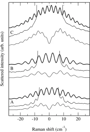
Figure 3 shows low-frequency Raman spectra mea-sured from the three GaAsN/GaAs multiple quantum well structures. As mentioned in section II, the nitro-gen concentration could be slightly different from sam-ple to samsam-ple and also in comparison with the measured value for the 1 µm thick GaAsN layer. For sample C, it is clearly non uniform: strong variations are observed along
the growth axis. Hence, the energy of the E+ transition
could depend on the sample. Therefore, the enhancement factor of the Raman scattering is not exactly the same for all samples since we used the same excitation energy (1.91 eV). This should also lead to selection of slightly different electronic densities. Though the output wave-length of the laser cannot be adjusted continuously, the
excitation is still close to resonance with the E+
transi-tion for all samples.
Periodic oscillations of the low-frequency Raman spec-tra are clearly observed for samples A and B (Fig. 3). They originate from the interference between the Raman scattering amplitudes associated with each GaAsN quan-tum well. Their period is determined by the longitudinal sound velocity and by the separation between quantum wells. Their relative intensities (spectral envelop) is a form factor given by the Fourier transform of the elec-tronic density distribution in each quantum well. The
-20 -10 0 10 20
Raman shift (cm-1)
Scattered intensity (arb. units)
A B C
FIG. 3: Calculated and measured Raman spectra of the GaAsN/GaAs quantum well structures. Optical excitation has been performed at 1.9 eV. The thickness of the GaAs spacers is 12 nm, 24 nm and 39 nm for samples A, B and C, respectively. The spectra calculated assuming either uniform (bold line) or localized (thin line) electron density distribution (see text) in the plane of the quantum wells are shown.
interference contrast is directly connected to the
inter-layer correlation of the electronic density.17,18 For
sam-ple C, the oscillations are hardly observable due to very weak interference contrast.
Calculated Raman spectra are presented in Fig. 3. The same scattering model as the one discussed for the thick GaAsN layer has been used. The only difference with the spectra in Fig. 2 is the spatial distribution of the resonant electronic wave-function. Instead of the three-dimensional distribution of impurities, now we have lay-ering of the wave-function along the growth direction.
Moreover, since the energy of the resonant a1(2) states
is above the GaAs CBM, quantum confinement effects are not expected. Then, we used an ensemble wave-function of randomly distributed nitrogen impurities in each GaAsN quantum wells with the parameters ` and d obtained from the thick GaAsN layer.
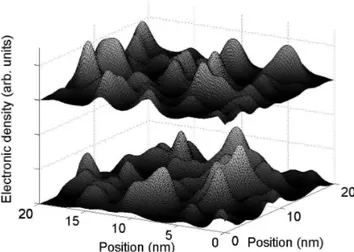
Figure 4 shows the in-plane electronic density in two of the five GaAsN/GaAs quantums wells. The param-eters, such as thickness of quantum wells and distance between quantum wells, were taken from the TEM im-ages in Fig. 1.
As one can see in Fig. 3, good agreement between cal-culated and measured spectra is obtained for samples A
6
FIG. 4: In-plane electron density distribution used for the calculations of the resonant Raman spectra. They are shown only for two GaAsN/GaAs quantum wells, and were gener-ated assuming coherent superposition of randomly distributed a1(2) states centered at the nitrogen impurities.
and B. The period and spectral envelop of the oscillations are well accounted for. As mentioned above, the inter-ference contrast is determined by the inter-well spatial correlation of the electronic density (Fig. 4). The spectra calculated for a uniform in-plane distribution of the elec-tronic density (` À d ) in each quantum well are shown for comparison. In this case, the interference contrast is maximum (totally delocalized states). The parameter l and d extracted from the thick GaAsN layer are indeed those which give the best agreement between calculated and observed interference contrast.
Sample C, shows a much weaker interference contrast. The nitrogen distribution along the growth axis is not
uniform for this sample (Fig. 1). Keeping in mind that
lo-calization and mixing of a1(2) PHS depend on the
nitro-gen concentration, the weaker interference contrast could be due to selection of strongly localized states (` ¿ d ) or to fluctuations of the nitrogen concentration in the plane of the quantum wells.
IV. CONCLUSION
Resonant Raman scattering, detected in the frequency range of acoustic phonons, reveals the spatial distribu-tion of the excited electronic density. We have applied this approach to the study of electronic wavefunction lo-calization in GaAsN. Our main findings can be summer-ized as follows. (i) By comparing calculated and mea-sured Raman spectra we have extracted the localization
length of those conduction states involved in the E+
op-tical transition, namely the a1(2) states. We found a
good agreement with the electronic structure predicted by the pseudo-potential supercell technique and by the large scale local density approximation. (ii) Impurity band formation has been adressed using an ensemble wavefunction for the calculations of the Raman spectra. (iii) Interference Raman effects were generated by lay-ering the electronic density along one direction (multi-ple quantum wells). We have observed a strong inter-ference contrast on two of the studied structures. This supports partial delocalization of the electronic density over many nitrogen impurities, i.e. band impurity
forma-tion of a1(2) states. The comparison between calculated
and measured low-frequency Raman spectra confirm the spatial distribution of the electronic density at the stud-ied nitrogen composition.
1 M. Weyers, M. Sato and H. Ando, Jpn. J. Appl. Phys. 31,
L853 (1992).
2
J. Salzman and H. Temkin, Mater. Sci. Eng. B 50, 148 (1997).
3
J. D. Perkins et al., Phys. Rev. Lett. 82, 3312 (1999).
4
W. Shan et al., Phys. Rev. Lett. 82, 1221 (1999).
5
E. D. Jones et al., Phys. Rev. B 60, 4430 (1999).
6 Y. Zhang, A. Mascarenhas, H. P. Xin and C. W. Tu, Phys.
Rev. B 61, 7479 (2000).
7
et al., Appl. Phys. Lett. 76, 2409 (2000).
8 W. Shan et al., Appl. Phys. Lett. 76, 3251 (2000). 9
W. Walukiewisz et al., Phys. Rev. Lett. 85, 1552 (2000).
10
L.Bellaiche, Su-Huai Wei and A. Zunger, Phys. Rev. B 54, 17568 (1996).
11
T Mattila, Su-Huai Wei and A. Zunger, Phys. Rev. B 60, R11245 (1999).
12 P. R .C. Kent and A. Zunger, Phys. Rev. Lett. 86, 2613
(2001).
13
P. R .C. Kent and A. Zunger, Phys. Rev. B. 64, 115208 (2001).
14 T. Ruf in Phonon Raman scattering in Quantum wells and
superlattices, 142 Springer, Berlin (1998).
15
W. F. Sapega et al., Solid. State Comm. 84 1039 (1992).
16 A. Mlayah et al., Phys. Rev. Lett. 78, 4119 (1997). 17
M. Cazayous et al., Phys. Rev. B 62, 7243 (2000).
18
M. Cazayous et al., Phys. Rev. B 64, 33306 (2001).
19
Lin.-Wang Wang, Appl. Phys. Lett. 78, 1565 (2001).
20 A. M. Mintairov et al., Phys. Rev. B. 56, 15836 (1997). 21
T. Prokofyeva et al., Appl. Phys. Lett. 73, 1409 (1998).
22
H. M. Cheong, Y. Zhang, A. Mascarenhas and J. F. Geisz, Phys. Rev. B 61, 13687 (2000).
23
J. Wagner et al., Appl. Phys. Lett. 77, 3592 (2000).
24
Y. Zhang et al., Phys. Rev. B 63, 085205 (2001).
25 M. J. Seong, M. C. Hanna and A. Mascarenhas, Appl.
Phys. Lett 79, 3974 (2001).
26
A. Hashimoto et al., J. of Cryst. Growth 227, 532 (2001).
27 J. Wagner et al., J. Appl. Phys. 90, 5027 (2001). 28
T. Geppert et al., Appl. Phys. Lett. 80, 2081 (2002).
29
G. Bachelier et al., Proceedings of the International Con-ference on the Physics of Semiconductors, 2002,
Edin-burgh.
30
H. Carr`ere, A. Arnoult, A. Ricard, and E. Bedel-Pereira, J. Cryst. Growth 243, 295 (2002).
31
L. W. Wang, L. Bellaiche, S. H. Wei and A. Zunger, Phys. Rev. B 80, 4725 (1998).
32
B. Jusserand and M. Cardona in Light Scattering in Solids
66, Springer, Berlin (1979).
33
H. Bilz and W. Kreiss in Phonon Dispersion Relations in Insulators, Springer, Berlin (1979).
34