Modeling, Development and Control of Multilevel Converters
for Power System Application
by
Hani VAHEDI
MANUSCRIPT-BASED THESIS PRESENTED TO ÉCOLE DE
TECHNOLOGIE SUPÉRIEURE IN PARTIAL FULFILLMENT FOR THE
DEGREE OF DOCTOR OF PHILOSOPHY
Ph.D.
MONTRÉAL, NOVEMBER 11
TH, 2016
ÉCOLE DE TECHNOLOGIE SUPÉRIEURE
UNIVERSITÉ DU QUÉBEC
It is forbidden to reproduce, save or share the content of this document either in whole or in parts. The reader who wishes to print or save this document on any media must first get the permission of the author.
BOARD OF EXAMINERS
THIS THESIS HAS BEEN EVALUATED BY THE FOLLOWING BOARD OF EXAMINERS
Mr. Kamal Al-Haddad, Thesis Supervisor
Department of electrical engineering, École de technologie supérieure Mr. Gabriel J. Assaf, Chair, Board of Examiners
Department of electrical engineering, École de technologie supérieure Mr. Ambrish Chandra, Examiner
Department of electrical engineering, École de technologie supérieure Mr. Luiz Lopes, External Examiner
Department of electrical engineering, Concordia University Mr. Ahmed Chériti, Independent External Examiner
Department of electrical engineering, Université du Québec à Trois-Rivières
THIS THESIS WAS PRESENTED AND DEFENDED
IN THE PRESENCE OF A BOARD OF EXAMINERS AND THE PUBLIC
ON NOVEMBER 7TH, 2016
ACKNOWLEDGMENTS
“Feeling gratitude and not expressing it is like wrapping a present and not giving it.”, William Arthur Ward (1921–1994).
Many people accompanied me during the endeavor of my doctoral studies and of writing this dissertation. I am deeply grateful for their support. First of all, I would like to thank my supervisor, Professor Kamal Al-Haddad, for showing me the joy of research, for shaping my path to research by guiding me with his extensive knowledge, for teaching me how to write, for his unending encouragement and support, and for becoming a friend. I hope that I could have done all my promises to him during my studies.
Great thanks go also to Dr. Nassar Mendalek for giving me his constructive comments and discussing on each part of this work.
I also had the chance to work with great researchers from whom I learned a lot. I thank Dr. Hadi Kanaan from Saint-Joseph University as well as Prof. Leopoldo Franquelo and Dr. Ramon Portillo from Univrsity of Sevilla.
I would also like to thank the members of my Ph.D. committee who enthusiastically accepted to review my dissertation. I am very thankful to all my colleagues at GREPCI for their feedback and the productive discussions. And special thanks go to my best teammate Philippe-Alexandre Labbé without whom I could not reach such great records of achievements in whole project.
I am very thankful to my whole family : To my mother who somehow convinced me that ‘failure’ is not a dictionary word ; to my father whom I never managed to explain what I do but who is always happy for my success ; to my sister, brother and parents-in-law who were always there for me. I love you all so much!
Last but certainly not least, I thank my beloved wife Azadeh for letting me pursuing my dreams. Thank for your unconditional support, for your patience, and understanding. Thank you for postponing your plans to catch up with mines. Thank you for loving me!
I also thank my little angel (my daughter Anita) who just born on June 13th 2016 and gave me
infinite source of energy by her endless smiles. She brought me all the luck by opening eyes to this beautiful word.
MODELING, DEVELOPMENT AND CONTROL OF MULTILEVEL CONVERTERS FOR POWER SYSTEM APPLICATIONS
Hani VAHEDI
ABSTRACT
The main goal of this project is to develop a multilevel converter topology to be useful in power system applications. Although many topologies are introduced rapidly using a bunch of switches and isolated dc sources, having a single-dc-source multilevel inverter is still a matter of controversy. In fact, each isolated dc source means a bulky transformer and a rectifier that have their own losses and costs forcing the industries to avoid entering in this topic conveniently. On the other hand, multilevel inverters topologies with single-dc-source require associated controllers to regulate the dc capacitors voltages in order to have multilevel voltage waveform at the output. Thus, a complex controller would not interest investors properly. Consequently, developing a single-dc-source multilevel inverter topology along with a light and reliable voltage control is still a challenging topic to replace the 2-level inverters in the market effectively.
The first effort in this project was devoted to the PUC7 inverter to design a simple and yet efficient controller. A new modelling is performed on the PUC7 inverter and it has been simplified to first order system. Afterwards, a nonlinear cascaded controller is designed and applied to regulate the capacitor voltage at 1/3 of the DC source amplitude and to generate 7 identical voltage levels at the output supplying different type of loads such as RL or rectifier harmonic ones.
In next work, the PUC5 topology is proposed as a remedy to the PUC7 that requires a complicated controller to operate properly. The capacitor voltage is regulated at half of dc source amplitude to generate 5 voltage levels at the output. Although the 7-level voltage waveform is replaced by a 5-level one in PUC5 topology, it is shown that the PUC5 needs a very simple and reliable voltage balancing technique due to having some redundant switching states. Moreover, a sensor-less voltage balancing technique is designed and implemented on the PUC5 inverter successfully to work in both stand-alone and grid-connected mode of operation.
Eventually, a modified configuration of the PUC5 topology is presented to work as a buck PFC rectifier. The internal performance of the rectifier is like a buck converter to generate stepped down DC voltages at the two output terminals while the grid sees a boost converter externally. As well, a decoupled voltage/current controller is designed and applied to balance the output voltages identically and synchronize the input current with grid voltage to have a PFC operation acceptably. A power balance analysis is done to show the load variation range limit.
All the theoretical and simulation studies are validated by experimental results completely.
Keywords: Cascaded Nonlinear Control, Multilevel Converter, Packed U-Cell, PUC5,
MODÉLISATION, DÉVELOPPEMENT ET CONTRÔLE DES CONVERTISSEURS MULTINIVEAU POUR LES SYSTÈMES DE PUISSANCE
Hani VAHEDI
RÉSUMÉ
Le but principal de ce projet est le développement d’une topologie d’onduleur multiniveau utile aux applications en puissance. Bien que plusieurs topologies différentes soient introduites, elles utilisent en général une multitude d’interrupteurs et de sources CC isolées. Avoir un convertisseur multiniveau avec une seule source CC est encore une technologie en développement. En fait, chaque source CC isolée représente un transformateur et un redresseur qui possèdent leurs propres pertes et prix et rendent la plupart du temps ses systèmes inintéressants pour l’industrie. D’un autre côté, les convertisseurs multiniveaux à source unique requièrent un contrôleur plus évolué pour réguler la tension des condensateurs flottants; un requis pour avoir la forme d’onde multiniveau en sortie. Or, un contrôleur est beaucoup moins intéressant pour un investisseur. Conséquemment, développer un onduleur multiniveau avec une seule source CC et un contrôle léger et robuste de la tension est encore un défi. Le remplacement des onduleurs à deux niveaux n’est pas pour tout de suite.
Le premier effort de ce projet est dévoué à l’onduleur PUC7 dans le design de son contrôleur afin qu’il soit simple et efficace. Le développement d’un nouveau modèle mathématique du PUC7 a été simplifié à un système du premier ordre. Par la suite, un contrôleur non linéaire en cascade est développé et appliqué pour réguler la tension des condensateurs au tiers de la tension d’alimentation. Cela permet de générer 7 niveaux de tension identiques à la sortie et peut alimenter des charges linéaires et non linéaires.
La topologie à cinq niveaux, le PUC5, est proposée pour remédier à la complexité du contrôleur du PUC7. La tension du condensateur flottant est régulée à la moitié de la tension d’alimentation afin de générer les niveaux de tension à la sortie. Malgré le nombre moindre de niveaux de tension, il est démontré que le PUC5 nécessite une technique de balancement très simple due à la redondance des niveaux de tension. De plus, une technique de balancement des condensateurs sans mesure de tension a été développée et implémentée en pratique sur le PUC5 en mode onduleur autonome et connecté avec le réseau électrique. Une configuration modifiée de la topologie PUC5 est en cours de développement afin de fonctionner comme un redresseur abaisseur avec PFC. Les performances de cette topologie en tant que redresseur est très semblable à un montage abaisseur. Cependant, le réseau voit le convertisseur comme un montage élévateur. Le contrôleur est conçu afin de balancer la tension de sortie et pour synchroniser le courant d’entrée avec le réseau. Un bilan de puissance est réalisé afin de démontrer les variations limites de la charge.
Toutes les simulations et résultats théoriques sont validés expérimentalement.
Mots-clés: Cascade de Contrôle Non-Linéaire, Converter Multiniveau, Packed U-Cell,
TABLE OF CONTENTS
Page
INTRODUCTION ... 1
CHAPTER 1 LITERATURE REVIEW OF MULTILEVEL INVERTERS ... 11
1.1 Introduction ... 11
1.2 Multilevel Inverter Topologies ... 13
1.2.1 Cascade H-Bridge ... 13
1.2.1.1 CHB with equal DC sources ... 14
1.2.1.2 CHB with unequal DC sources ... 15
1.2.2 Neutral Point Clamped ... 16
1.2.3 Flying Capacitor ... 18
1.2.4 Generalized Multilevel Inverter... 18
1.2.5 Five Level H-Bridge Neutral Point Clamped ... 19
1.2.6 Three Level Active Neutral Point Clamped ... 20
1.2.7 Modular Multilevel Converter ... 21
1.2.8 Three-Level T-Type Inverter ... 22
1.2.9 Packed U Cell ... 23
1.2.10 Pinned Mid-Points (PMP) ... 24
1.2.11 Crossover Switches Cell (CSC) ... 24
1.2.12 Other Multilevel Inverter Topologies ... 25
1.3 Switching Techniques of Multilevel Inverters ... 30
1.3.1 Pulse Width Modulation ... 30
1.3.1.1 Level-Shifted PWM ... 32
1.3.1.2 Phase-Shifted PWM ... 34
1.3.2 Space Vector Modulation ... 34
1.3.3 DC Voltage Balancing ... 37
1.4 Modeling and Control of Multilevel Inverter ... 37
1.5 State of The Art (Impact on Industry) and Originality of the research ... 38
1.6 Conclusion ... 42
CHAPTER 2 REAL-TIME IMPLEMENTATION OF A SEVEN-LEVEL PACKED U-CELL INVERTER WITH LOW SWITCHING FREQUENCY VOLTAGE REGULATOR ... 43
2.1 Introduction ... 43
2.2 PUC Inverter Modelling and Controller Design ... 45
2.3 Experimental Results ... 54
CHAPTER 3 SENSOR-LESS FIVE-LEVEL PACKED U-CELL (PUC5) INVERTER OPERATING IN STAND-ALONE AND
GRID-CONNECTED MODES ... 59
3.1 Introduction ... 59
3.2 Proposed PUC5 Inverter Topology and Self-Voltage-Balancing Switching Technique ... 61
3.2.1 PUC5 Inverter Configuration and Sensor-Less Voltage Balancing Investigation ... 61
3.2.2 Sensor-Less Voltage Controller Integrated Into Switching Technique ... 68
3.3 Grid-Connected Mode Configuration and Controller ... 70
3.4 Comparative Study of Multilevel Inverter Based on Number of Components ... 71
3.5 Experimental Results ... 74
3.5.1 Test 1: Stand-Alone Mode ... 74
3.5.2 Test 2: Grid-Connected Mode ... 77
3.5.3 Test3: 3-Phase PUC5 inverter ... 81
3.6 Conclusion ... 83
CHAPTER 4 A NOVEL MULTILEVEL MULTI-OUTPUT BIDIRECTIONAL ACTIVE BUCK PFC RECTIFIER ... 85
4.1 Introduction ... 85
4.2 Proposed PFC Buck Rectifier Topology and Operation Principle ... 87
4.3 Switching Technique and Integrated Voltage Regulator ... 90
4.4 Implemented Controller ... 92
4.5 Power Balance Analysis ... 93
4.6 Experimental Results ... 100
4.7 Conclusion ... 104
CONCLUSION ... 105
APENDIX I PROOF OF SELF-VOLTAGE-BALANCING IN PUC5 INVERTER ... 111
APENDIX II DESIGN CONSIDERATION OF THE PUC5 INVERTER ... 115
LIST OF TABLES
Page
Table 1.1 Switching States of one phase of a 3L-NPC ... 35
Table 2.1 Switching States and Voltage Levels of the PUC Inverter ... 47
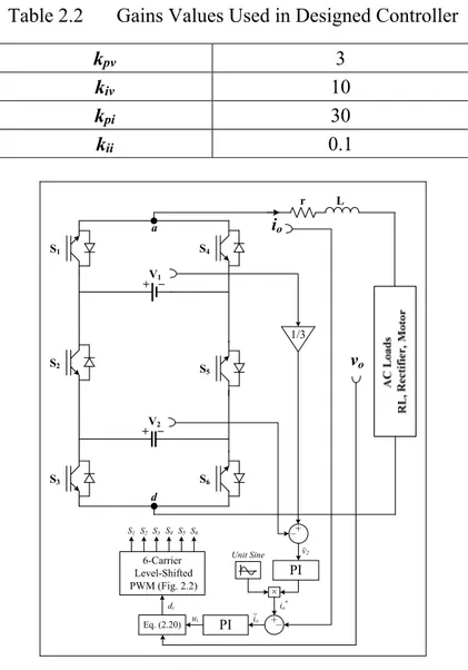
Table 2.2 Gains Values Used in Designed Controller ... 53
Table 2.3 System Parameters Used in Practical Tests ... 55
Table 3.1 All possible switching states of PUC Inverter ... 62
Table 3.2 PUC5 Capacitor voltage states ... 64
Table 3.3 Components count for single-phase five-level inverters ... 72
Table 3.4 Components count for single-phase multilevel inverters ... 72
Table 3.5 Experimental system parameters ... 74
Table 4.1 Switching States of the proposed Five-Level Buck PFC Rectifier ... 89
Table 4.2 Effect of Switching States On Output DC Capacitors ... 91
LIST OF FIGURES
Page
One leg of a) 2-level, b) 3-level and c) n-levels inverter ... 12
7-Level CHB ... 14
The output voltage waveform of phase a in a 7L-CHB with equal DC sources ... 15
The output voltage waveform of phase a in a 15L-CHB with unequal DC sources ... 16
Phase ‘a’ of a Three Level NPC ... 17
One Phase of a Three-Level FC Multilevel Inverter ... 18
Generalized multilevel inverter topology ... 19
5L-HNPC multilevel inverter ... 20
3L-ANPC with Active Clamped Switches ... 21
Modular Multilevel Converter (MMC) ... 22
3L-NPP ... 22
Single-Phase 7L-PUC... 23
Three-phase 5-level PMP inverter ... 24
9-Level CSC inverter topology ... 25
Simplified five-level inverter ... 26
Five-level coupled inductance inverter ... 27
Five-level inverter using half-bridge cells ... 28
Multilevel inverter using half-bridge and three-phase VSI ... 28
Seven-level hybrid multilevel inverter using HB cell to change the polarity ... 29
Sinusoidal PWM ... 31
Level Shifted PWM Carriers for 5L Inverter: a) IPD , b) APOD , c)POD ... 33
Phase Shifted PWM Carriers for 7L-CHB ... 34
Sectors and Regions in SVM for 3L-NPC ... 36
GCT-based 3L-NPC drive by ABB (ACS1000) ... 40
IGBT 11L-CHB drive by ASI Robicon ... 40
3L-NPC for wind power conversion by ABB (PCS-6000-wind) ... 41
3L-NPC for wind power conversion by Converteam (MV7000) ... 41
MMC for HVDC with its Control System and Cooling System ... 42
Single-phase PUC Inverter ... 46
Multicarrier PWM for 7-level PUC inverter ... 50
Block diagram of proposed controller applied on 7-level PUC inverter ... 53
PUC inverter voltage and current waveforms in steady state condition ... 55
Voltage regulation during a fast 66% increase in DC source amplitude ... 56
Adding a nonlinear load (rectifier) to the PUC inverter while supplying an RL load ... 57
PUC5 Inverter Topology ... 62
Switching states and conducting paths of PUC5 inverter ... 64
Typical output voltage and current waveform of a five-level inverter ... 66
Five-level PWM scheme using four vertically shifted carrier waveforms ... 69
XVII
Proposed open-loop switching algorithm for
self-voltage-balancing of PUC5 Inverter ... 70
Grid-connected PUC5 inverter with designed controller ... 71
Components count chart in multilevel inverters ... 73
Start-up capacitor charging, 5-level voltage generating and FFT analysis ... 75
Adding single-phase rectifier as nonlinear load to the output of PUC5 ... 76
DC source voltage changes and capacitor voltage is tracking the reference value ... 78
Switches gate pulses ... 78
Grid-connected PUC5 with change in current reference amplitude ... 79
THD, and Crest factor computation of injected grid current ... 80
PUC5 operation at different power factors a) PF = 0.86, θ = 30° b) PF = 0.86, θ = 60° ... 81
3-Phase PUC5 inverter ... 82
Phase, Line and Load voltage waveforms of 3-phase PUC5 inverter ... 83
3-Phase line voltages of PUC5 inverter ... 83
Proposed five-level buck PFC rectifier ... 89
Operating sequences and conducting paths of proposed 5-level buck rectifier ... 90
Input/output signals of PWM block with integrated voltage regulator ... 92
Block diagram of the proposed rectifier and Implemented controller ... 93
Split configuration of the proposed rectifier into two cells for
power balance analysis ... 94 a) one line diagram of the 5-level rectifier b) Phasor diagram of
the system voltages ... 96 a) stable operation area of the rectifier b) Minimum and maximum
power generated by each cell and associated voltages ... 97 Stable and unstable operation of the proposed rectifier a) DC
voltages and input active power during changes in the loads b) grid voltage/current and rectifier 5-level voltage when R1 = R2 =
43Ω| c) grid voltage/current and rectifier 5-level voltage when R1
= 15Ω and R2 = 43Ω d) grid voltage/current and rectifier 5-level
voltage when R1 = 8Ω and R2 = 43Ω ... 99
Experimental results of the proposed rectifier connected to 120V RMS AC grid and supplying two DC loads at 125V DC. a) Output DC voltages regulated at 125V with grid side synchronized voltage and current b) DC loads currents with grid side synchronized voltage and current c) 5-Level voltage waveform at the input of the rectifier d) RMS and THD values of the AC side
synchronized voltage and current waveforms ... 101 Test results during 200% increase in Load1 from 53Ω to 160Ω ... 102
Test results during 50% decrease in Load2 from 80Ω to 40Ω ... 103
Supply voltage variation while the output DC voltages are regulated at 125V as buck mode of operation. ... 104
LIST OF ABREVIATIONS
AC Alternative Current
APOD Alternative Phase Opposite Disposition
CHB Cascaded H-Bridge
CSC Crossover Switches Cell
DC Direct Current
FB Full Bridge
FC Flying Capacitor
FFT Fast Fourier Transform
HB Half Bridge
IPD In-Phase Disposition
KVL Kirchhoff's Voltage Law
NPC Neutral Point Clamped
PF Power Factor
PFC Power Factor Correction
PI Proportional Integral
POD Phase Opposite Disposition
PUC5 5-Level Packed U-Cell
PUC7 7-Level Packed U-Cell
PWM Pulse Width Modulation
SHE Selective Harmonic Elimination
SHM Selective Harmonic Mitigation
SPS SimPowerSystem
INTRODUCTION
The volume of the energy generation and distribution systems have increased significantly in recent years (Leopoldo G. Franquelo, 2012). Based on energy statistics shown in Figure 0.1, the world electricity energy consumption is increasing continuously that requests more power generation especially from renewable energy resources (wind and solar) (Enerdata, 2015). As a statistical outlook (British-Petroleum, January, 2013), total electricity consumption will be 61% higher in 2030 than in 2011. Besides, renewable energy reaches a 6% share of global energy production by 2030, up from 2% in 2011. Renewable energy resources play an important role in generating power due to green energy and low environmental impacts. However, their output is not useable by consumers and needs to be boosted and converted into a smooth AC waveform to deliver desired power to the grid with low harmonics which needs high power inverters with higher efficiency. Moreover, the industries demand higher power equipment which are more than megawatt level such as high power AC drives which are usually connected to the medium voltage networks (2.3, 3.3, 4.16 and 6.9 kV) (Rodriguez, Lai et Peng, 2002).
The output of a conventional 2-level inverter is just +Vdc or –Vdc from a DC capacitor with
the voltage magnitude of Vdc that has a lot of harmonics which is vital to be filtered.
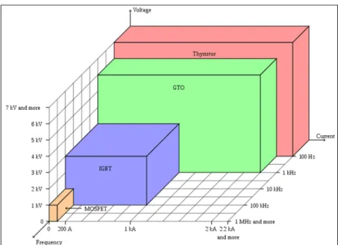
Regarding these values, the switches have to suffer high amount of voltage and current if such type of inverter is used in high power applications such as mining applications, high power motor drives, PV or Wind farm energy conversion systems and etc. On the other hand, high frequency operation is also limited for high power applications due to increased power losses. Moreover, it is required to use high voltage switches which are limited by the existing technologies as shown in Figure 0.2 (Wikipedia, 2012). One solution to overcome that limitation is using more switches and capacitors in series that can divide the voltage among the switches which is shown in Figure 0.3, but that increases the number of components significantly which need more DC isolators and physical space for the converter consequently (Rodríguez et al., 2007).
Figure 0.1 Electricity energy statistics in the world since 2005 0 5000 10000 15000 20000 25000 2005 2006 2007 2008 2009 2010 2011 2012 2013 2014 2015
Electricity Consumption (TWh)
0 5000 10000 15000 20000 25000 2005 2006 2007 2008 2009 2010 2011 2012 2013 2014 2015Electricity Production (TWh)
0 2 4 6 2005 2006 2007 2008 2009 2010 2011 2012 2013 2014 2015Share of Wind and Solar
in Electricity Production (%)
3
Figure 0.2 Existing technologies of semiconductor devices in power electronics applications (Wikipedia, 2012)
Figure 0.3 High Power VSI with series elements (switches with same names are fired coincide)
S1 S2 a S3 S4 S5 S6 b c S1 S1 S3 S3 S5 S5 S2 S2 S4 S4 S6 S6 Vdc/3
Motivation and Challenges
To resolve the above-mentioned problems, the new technology of inverters called Multilevel Inverters has been introduced employing combination of switches and DC sources to produce various voltage levels, which is being used in medium-voltage high-power applications (Rodríguez et al., 2007). Those switches are turned on and off with a pattern to produce desired combination of DC voltages at the output, while the switches are not suffering the whole DC voltage and they are just blocking a part of the DC bus. As well, producing smoother waveform leads to lower harmonic which reduces the filter size and power losses remarkably. So having less number of switches and isolated DC sources since generating high number of voltage levels at the output is always a matter of controversy where single-DC-source topologies are being considered the most suitable ones for most of the power system applications such as renewable energy conversion systems.
As large number of active switches, DC sources and capacitors are used in multilevel converters, more complicated control strategy should be designed to stabilize the voltage and keep the dynamic performance acceptable in both stand-alone and grid-connected mode of operation during healthy and faulty conditions.
Moreover, due to employing more semiconductor devices by multilevel inverters, the necessity of the modulation techniques with lower switching frequency and better performance has increased. There would be another challenge to develop the switching methods or propose new techniques in order to deal with the complex structure of multilevel inverters while balancing the auxiliary DC capacitors voltages used to increase the number of voltage levels at the output. Such voltage balancing techniques integrated into switching approaches remove the need of applying complicated external linear/nonlinear controllers to regulate the dependent DC links voltages.
Eventually, the rectifier (AC to DC conversion) mode of operation is so important for multilevel converters where low harmonic contents, low switching frequency and lower voltage rating of switches help producing a high DC voltage link with high power delivery to the batteries as one of the most challenging issues in EV charging applications.
5
Research Objective
Multilevel converter structure permits to generate smoother output waveform by producing different voltage levels while operating at lower switching frequency which leads to lower power losses in the power inverter and reduce the output filter size. Nowadays, the usage of such inverters has been reported up to 13.8 kV and 100 MW. In such power ratings various applications for such topologies can be mentioned, e.g.: mining applications, adjustable speed drives, renewable energy conversion, utility interface devices, reactive power compensators and etc. Moreover, multilevel rectifiers could be also used in high power applications such as newly emerged high power and super-fast chargers for EVs. The major weakness of conventional converters is limited power rating, high harmonic pollution and high switching frequency which prevents their usage when it comes to high power applications. Besides, in high power applications, the lower switching frequency is more desired to decrease the switching losses. Lower harmonic contents of voltage and current waveforms are also mandatory to reduce the size of output filters.
This project will present an improved multilevel inverter topology that can be used in high power medium voltage applications and remit the problem of using power electronics switches in high power ratings. Moreover, the low dynamic of such devices can be improved using advanced modelling and control techniques as will be proposed.
The research objectives can be summarized as the following:
• Designing and implementation of advance controllers for multilevel inverters;
• Developing voltage balancing techniques to integrate into switching pattern in order to regulate the DC capacitor voltage in multilevel inverters;
• Developing a multilevel inverter topology to work in stand-alone and grid-connected mode of operation reliably;
Methodology
This research has been performed in three following steps: mathematical modeling, simulation and hardware implementation.
At first literature review has been done to better understand the problems associated with multilevel converters. A thorough study has been performed about different multilevel converter topologies taking into account the number of active and passive devices, applied control strategies and switching techniques associated with the capacitor voltage balancing issue. In this step, existing models, controller, switching techniques and topologies have been simulated in Matlab/Simulink SPS toolbox to facilitate analyzing the advantages and disadvantages of those reported technologies.
The mathematical modeling of the existing and proposed topologies has been done to study the switching performance and design the advanced controllers. The developed topologies have been simulated in SPS with applied controllers to verify the good dynamic performance in stand-alone and grid-connected mode of operation. All possible transient modes such as load changing and AC or DC voltage variation have been investigated through the simulation to prevent any failure in hardware implementation.
Finally, proposed converters have been designed and made in the lab to test practically. Controllers and switching techniques have been implemented on dSpace1103 for rapid control prototyping. The OPAL-RT voltage/current measurement box has been used to sense the electrical variables and to send required information to the controller.
Thesis Contribution
The major contributions of this thesis are as the following:
Development of an improved model for the PUC7 inverter
In previous works the PUC7 inverter had been modeled based on separate switching actions. That means the concept of single input system for single-phase inverter had not been considered in modeling and controller design. Therefore, each switch was fired separately
7
without noticing the action on other switches. In this work a new model has been obtained for PUC7 inverter taking into account all switching states as a group of switching pulses. Therefore, no switch works individually and a set of switches are turned on/off together to generate the desired voltage level at the output. The new model complies with the mentioned concept of single input for single-phase converters. Thus, the controller could be designed using a single input to the inverter which would be modulated by PWM block to send the corresponding pulses.
Design of a low switching frequency controller for PUC7 inverter
PUC7 inverter was proposed in 2009 on which a feedback linearization control had been applied using that modeling with separate switching actions. Such process has the risk of missing some commutations at the right time results in producing a wrong voltage level. Afterwards, a hysteresis controller had been also implemented on the PUC7 inverter which has its own drawbacks such as high and variable switching frequency. In this project, new nonlinear controller has been designed and implemented on the PUC7 inverter based on the improved modeling. The applied controller does not need a new feedback from the system so it uses the existing data sent from adjusted sensors to compensate the nonlinearities of the converter model. Such robust controller allowed the PUC7 inverter to operate at low switching frequency while showing acceptable results. Moreover, the new nonlinear cascaded controller could be applied on all converters with voltage and current control loops like rectifiers or grid-connected inverters. Compared to a cascaded PI Controller, the designed nonlinear one shows better operation on all single-phase converters with fast error tracking while does not increase the complexity of calculations and implementation.
Design of a new multilevel inverter topology (PUC5)
After full investigation of PUC7 and analyzing its drawbacks, the PUC5 topology has been proposed in this thesis with most reliable performance and easy to use in various applications. The modified topology needs less number of switches considering the equal voltage rating and generates 5 voltage levels at the output with voltage THD of about 10% which is at least 10 times less than a 2-level waveform harmonics. The main feature of the
PUC5 topology is the fact that there are some redundant switching states which can be used for easy voltage balancing of the DC link capacitor. Due to new voltage rating of the switches, the PUC5 inverter could be implemented by 4 half-bridge modules.
Development of a sensor-less voltage balancing technique integrated into PWM switching block for PUC5 inverter
The most promising feature of PUC5 topology is the ability of balancing its DC link capacitor without using any voltage sensor as feedback to the controller. In fact, the auxiliary capacitor voltage is balanced using redundancy switching states but no voltage sensor or observer. It has been proved mathematically and experimentally that the capacitor voltage maintains the desired level during switching actions by the proper time of charge and discharge of energy. The applied technique makes the PUC5 inverter a strong potential to replace existing full-bridge converter in the market.
Design of a new multilevel buck PFC rectifier topology
The 5-level buck PFC rectifier topology has been proposed after a thorough analysis of rectifier mode of operation in multilevel converters. It generates two output DC voltages that help getting a boost operation from grid point of view. The sum of two DC voltages should be more than the AC main voltage thus the rectifier could work in boost mode while producing two output terminals in buck mode with reduced voltages. A decoupled voltage/current controller has been designed to operate the rectifier in all conditions such as AC source fluctuation or load changes. Moreover, a voltage balancing analysis has been performed mathematically and then based on simulation studies to validate the good dynamic performance of the proposed rectifier.
Thesis Outline
This thesis includes 5 chapters starting from literature review on multilevel converter topologies and switching technique and continuing on proposed topologies and controllers. CHAPTER 1 includes a comprehensive review on the previously reported the multilevel converter topologies and switching techniques. CHAPTER 2 shows an improved modeling of
9
the PUC7 along with designing and implementing procedure of a nonlinear cascaded control. Experimental results are illustrated to validate the good dynamic performance of the applied controller operating at low switching frequency. The PUC5 topology with sensor-less voltage control is introduced in CHAPTER 3 with experimental results of stand-alone and grid-connected mode of operation. The theoretical studies are done to prove the ability of PUC5 configuration in self-voltage-balancing of the DC link capacitor. The 5-level buck PFC rectifier is elaborated in CHAPTER 4 with all details on designing the decoupled voltage/current controller and switching technique. Moreover, the power sharing issue between output terminals of the rectifier is analyzed and described exhaustively in this part. Simulation and experimental results validate the promising functionalities of the proposed 5-level buck PFC rectifier. CHAPTER 5 concludes the thesis and gives some ideas for future studies.
CHAPTER 1
LITERATURE REVIEW OF MULTILEVEL INVERTERS 1.1 Introduction
The multilevel converter technology has been started by the concept of multilevel step wave in cascade H-Bridge converters in the late 1960s. This was an attempt to present a new control method that was useful to produce and employ the stepped wave at the output of such inverters (McMurray, 1971). The circuit of that type of cascade H-bridge converter was presented in (Bedford et Hoft, 1964). In 1970, the Diode Clamped Converter was introduced (Baker, 1980) but all these efforts was done in low power applications.
In medium-voltage application the Neutral Point Clamped (NPC) and then the Cascade H-Bridge (CHB) have been introduced in 1980s (Baker, 1981; Nabae, Takahashi et Akagi, 1981). In addition to these two types, the Flying Capacitor (FC) inverter which was introduced in 1960 as a low voltage one, has been evolved to be employed in medium-voltage and high power industries in 1990 (Meynard et Foch, 1991).
As an application example of such devices is medium-voltage motor drive that was begun in the middle of 1980s when the 4500 V gate turn off (GTO) thyristors were commercialized (Wu, 2006). Afterwards, development of high power switches results in manufacturing insulated gate bipolar transistor (IGBT) and gate commutated thyristor (GCT) in the late 1990s (Steimer et al., 1997). These switches have been employed in medium-voltage and high power inverters rapidly because of their appeal characteristics, low power losses, simple gate control and snubberless operation (Wu, 2006).
One leg of a) 2-level, b) 3-level and c) n-levels inverter
Multilevel inverter contains several semiconductor switches and DC supplies. The combination of switches actions produces various voltage levels at the output. Figure 1.1 shows the basic concept of a multilevel inverter operation. It shows the DC link and one leg of inverter in two-level, three-level and n-level configuration. The performance of semiconductor switches is shown by ideal switches. Figure 1.1-a shows a conventional inverter which can produce +Vdc or –Vdc at the output point of ‘a’ with respect to the
grounded neutral point, while the three-level inverter in Figure 1.1-b produces +Vdc, 0 and –
Vdc at the output and finally the n-level inverter in Figure 1.1-c generates multilevel voltages
of 0, ±Vdc, ±2Vdc, … . As it is obvious from the figure, the semiconductor switches suffer
only Vdc or less, however the output maybe more than Vdc. This feature of multilevel inverter
helps the industries and renewably resources to reach high power demands and applications using medium-voltage equipment.
Recently, multilevel inverters are gathering the researchers and industries attention due to their attractive features. Some of the major advantages of multilevel inverters are as follows (Kouro et al., 2010; Leopoldo G. Franquelo, 2012):
• Lower distortion in the output voltage due to multiple levels of output waveform; • Lower dv/dt (voltage stress) that leads to endure the reduced voltage by switches;
... ... ...
13
• Lower common mode voltage which is helpful in motor drives; • Lower switching frequency results in lower switching losses.
Different types of multilevel inverters have been proposed and built which are mostly for medium-voltage and high power applications (Franquelo et al., 2008) because of the fact that a single power switch cannot be connected to a medium-voltage grid directly.
1.2 Multilevel Inverter Topologies
Different topologies have been proposed for multilevel inverters (Franquelo et al., 2008; Kouro et al., 2010; Rodriguez, Lai et Peng, 2002) which are mentioned as follows.
1.2.1 Cascade H-Bridge
The cascade H-Bridge (CHB) multilevel inverter is mostly used in medium-voltage high power drives (Wu, 2006). CHB is composed of multiple units of single-phase H-Bridge (HB) inverter which are connected in series in each phase. Figure 1.2 shows the one phase of a 7-level CHB (7L-CHB) that includes three single-phase HB cell in each phase (Malinowski et al., 2010).
In a CHB multilevel inverter the output voltage of each phase is: Van=V1+V2+V3
There are two types of CHB: One with equal DC sources and another with unequal DC sources which are described below.
7-Level CHB
1.2.1.1 CHB with equal DC sources
Assume that Vdc1=Vdc2=Vdc3=E. To determine the number of levels in this mode the
following equation can be used:
L=2N+1
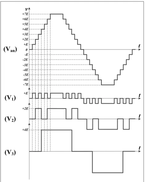
Where, L is the number of inverter levels or the output phase voltage levels. N is the number of HBs in each leg. For the Figure 1.2, there are three HBs in each leg so the CHB is a seven level inverter. The levels of inverters show the output voltage levels., so in this case, it means that the 7L-CHB in Figure 1.2 with equal DC sources would have the voltage values of 0, ±E, ±2E and ±3E which is shown in Figure 1.3 (Liu, 2009).
15
The output voltage waveform of phase a in a 7L-CHB with equal DC sources
1.2.1.2 CHB with unequal DC sources
Another type of CHB is with unequal DC sources. For instance, in Figure 1.2, consider that Vdc1 = E, Vdc2 = 2E and Vdc3 = 4E, so the combination of voltages results in 15 voltage levels
for Van which is shown in Figure 1.4. The maximum of 7E is produced while the output
waveform is more similar to the sine wave with fewer harmonics.
As it is obvious from the figure 3-4, using unequal DC sources leads to more voltage levels and higher output voltages with higher power in comparison with a CHB that has the same number of cells. But CHB with unequal DC sources needs more difficult switching pattern design because of the reduction in the redundant switching states which limits the application of this type of multilevel inverter in industries (Wu, 2006). The highest levels achieves when the DC sources values are triple (Lai et Shyu, 2002; Liu et Luo, 2005). For example, if Vdc1 =
E, Vdc2 = 3E and Vdc3 = 9E, then the output voltage levels will be up to 27 that can boost the
output voltage to 13E and eliminates many harmonics.
The output voltage waveform of phase a in a 15L-CHB with unequal DC sources
1.2.2 Neutral Point Clamped
Figure 1.5 shows one leg of a Neutral Point Clamped (NPC) multilevel inverter which was first introduced by Nabae (Nabae, Takahashi et Akagi, 1981) and then, the three-level NPC has found many developments and usage in industries (Rodriguez et al., 2010).
t v +E +2E +3E 0 -E -2E -3E
(V
an)
(V
1)
(V
2)
t t(V
3)
t +4E +5E +6E +7E -4E -5E -6E -7E +E +2E +4E17
Phase ‘a’ of a Three Level NPC
The clamped diodes (D1a, D2a) are connected to the neutral point of DC capacitors that results
in adding a zero level to the output voltage. Thus, in a 3L-NPC the output voltage is composed of -Vdc, 0 and +Vdc. when S1a and S2a are ON, the output is + Vdc. when S3a and S4a
are ON, the negative voltage will be appear at the output which is -Vdc. finally, if S2a and S3a
are ON, the voltage at ‘a’ will be 0. S3a is working in complementary of S1a and the same for
S2a and S4a. For instance, when S1a is ON, S3a is OFF.
One of the advantages of this topology is its flexibility for being controlled by space vector modulation (SVM) (Lewicki, Krzeminski et Abu-Rub, 2011; Rojas, Ohnishi et Suzuki, 1995) in addition to PWM. This feature makes the NPC as a desired topology for multilevel inverter for researchers to work on its control strategy and propose and test many control methods (Das et Narayanan, 2012; Lin et Wei, 2004). However the NPC is widely used in high power applications, balancing the capacitors voltages and unequal loss distribution among switches are considered as a drawback of this topology (Rodriguez et al., 2010).
1.2.3 Flying Capacitor
Another topology for multilevel inverters is Flying Capacitor (FC) which is observable in Figure 1.6 (Escalante, Vannier et Arzandé, 2002).
One Phase of a Three-Level FC Multilevel Inverter
The clamped diode in NPC has been replaced by a capacitor in FC model. It is derived from a two level inverter that each two switches are supplied by a capacitor. This topology produces three levels of voltages at the output which are +Vdc, 0, - Vdc. Due to employing many
capacitors in FC, it needs a large number of isolators for DC capacitors and a complex voltage balancing control which limits its practical use (Wu, 2006).
In addition to these topologies, some new topologies are currently have found practical applications and these are mentioned in continue (Kouro et al., 2010).
1.2.4 Generalized Multilevel Inverter
The generalized structure was introduced by Peng in 2001 (Peng, 2001). This topology has ability to balance the capacitor voltage itself. As it is illustrated in Figure 1.7, this configuration can be expanded easily and generate more levels while self-balancing the voltage.
19
Generalized multilevel inverter topology
Being symmetrical allows deriving many other configurations from this complete configuration e.g. NPC and FC. On the other hand, using too many switches and capacitors is a limitation of this topology. However, it is a good reference of switch combinations to study and analyze the multilevel inverter structures that can result in proposing new topologies with less components and self-voltage-balancing feature.
1.2.5 Five Level H-Bridge Neutral Point Clamped
The Five Level H-Bridge Neutral Point Clamped (5L-HNPC) contains two 3L-NPC leg connected in H-Bridge format in each phase, which was first introduced in 1990 (Wu, Lau et Chung, 1999) and have been developed later (Cheng et Wu, 2007). This type of combinations is called hybrid multilevel inverters. As shown in Figure 1.8, there are lots of semiconductors that make the switching method more complicated while the output voltage is a five-level waveform and produce more power up to 120 MVA (Kouro et al., 2010).
5L-HNPC multilevel inverter
Assume that V1 = V2 = V3 = 2E and each capacitor has a voltage of E. so the output of NPC
would be +E, 0, -E and the output of the 5L-HNPC is 0, ±E, ±2E.
1.2.6 Three Level Active Neutral Point Clamped
One of practical issues with NPC is the unequal semiconductor distribution losses due to non-identical voltage stress on switches leads to asymmetrical heat sink for these switches. Moreover, there would be some junctions with different temperature in NPC structure. This issue can be solved by replacing the clamping diodes in NPC with clamping semiconductor switches. These active clamping switches make controllable path for current through the neutral point and other switches, hence the losses distribution can be controlled significantly (Bruckner, Bernet et Guldner, 2005). Figure 1.9 shows the 3L-ANPC.
21
3L-ANPC with Active Clamped Switches
1.2.7 Modular Multilevel Converter
Modular Multilevel Converter (MMC) is composed of multiple cells of single-phase half-bridge or full-half-bridge inverters in modular structure. This topology is mostly used for transmission systems, particularly in HVDC (Gemmell et al., 2008). Figure 1.10 shows a MMC that contains a lot of cells. As it is shown in the phase ‘a’ of the figure, each cell consists of two semiconductor switches which are controlled by complementary pulses. These cells produce their DC voltage at the output so there would be an array of these DC voltages that makes multilevel voltage at the main output of phases (Kouro et al., 2010). Modularity of the MMC allows adding levels to reach medium and high voltage levels.
Modular Multilevel Converter (MMC)
1.2.8 Three-Level T-Type Inverter
A Three-Level T-Type inverter has been proposed in (Guennegues et al., 2009) which is similar to ANPC and shown in Figure 1.11.
3L-NPP
In that topology, each leg is connected to the neutral point through a bidirectional switch based on two anti-series connected IGBTs. Due to controllable path to the neutral point, the
23
switching losses can be distributed equally. The zero level is achieved when these two IGBTs are ON. This topology can work in higher frequency due to distributed switching losses and would be suitable for variable high speed applications such as train traction drives (Kouro et al., 2010).
1.2.9 Packed U Cell
A single-phase seven level Packed U Cells (PUC) multilevel converter has been illustrated in Figure 1.12 (Al-Haddad, Ounejjar et Gregoire, 2010; Ounejjar, Al-Haddad et Grégoire, 2011). This topology is a combination of FC and CHB with reduced number of capacitors and semiconductors.
Single-Phase 7L-PUC
As it is obvious in Figure 1.12, there are just six switches and two DC buses to produce seven levels of voltages at the output. The higher voltage is produced by the switch with lower switching frequency results in suppressing the switching stress significantly. Using the value of Vdc/3 for the capacitor voltage (Cdc) leads to generate the output voltage levels of 0,
1.2.10 Pinned Mid-Points (PMP)
The PMP multilevel inverter topology has been shown in Figure 1.13 (Vahedi, Rahmani et Al-Haddad, 2013). It is a modification on T3 inverter in which for the higher levels there is no need to add bidirectional switches and only one single switch would be enough.
Three-phase 5-level PMP inverter
It has the advantages of NPC and T-type topologies such as common DC bus for all phases but the main issue is the voltage balancing when a single-dc-source is used and 4 capacitors voltages should be regulated effectively.
1.2.11 Crossover Switches Cell (CSC)
The CSC inverter illustrated in Figure 1.14 has been developed (Vahedi et al., 2013)as a combination between CHB and PUC in which a single-dc-source is used and the auxiliary capacitor is controlled to have a maximum voltage at the output. Some similar efforts have been done on CHB to use a single-dc-source (Vahedi et Al-Haddad, 2015b; Vahedi et al.,
25
2015b). The output peak voltage is the sum of DC source and DC capacitors levels but there are some limitations on the modulation index.
9-Level CSC inverter topology
It generates the highest number of levels among other reported multilevel inverter topologies while using only a single-dc-source and 10 switches.
1.2.12 Other Multilevel Inverter Topologies
In addition to the above-mentioned topologies, so many other ones are proposed and reported in the literature which exceeds size of this report. Some of new introduced topologies are illustrated as the following.
Figure 1.15 shows a five-level inverter (Abd Rahim, Mohamad Elias et Hew; Ceglia et al., 2006). In this topology a HB with two dc capacitors are used that the capacitors’ middle point
is connected to the load by an auxiliary switch and four clamping diodes. The auxiliary circuit makes the other two levels in beside to the three-level output of a single HB. So, the output of proposed inverter will be a five-level wave (±Vs, ±Vs/2, 0).
Simplified five-level inverter
The above topology generates the higher value of Vs which is equal to its DC supply as well as the switching frequency of the implemented model was high, so it cannot be used in high-power applications.
Another five-level inverter topology has been introduced in (Li et al., 2012) using coupled inductance and a HB. Figure 1.16 shows the circuit of this inverter. A single HB can generate three voltage levels, while the coupled inductances make it possible to generate more voltage levels. These inductances can divide the output voltage into half of the main DC source. So the output includes 5-levels (±2E, ±E, 0). But it has the same problem as the previous topology in generating higher voltages than the DC source.
27
Five-level coupled inductance inverter
A five-level inverter is shown in Figure 1.17 (Waltrich et Barbi, 2010). Each phase is composed of four cells and each cell is a half-bridge inverter. The connection structure of the cells is clear in the figure. Since each phase generates a five-level waveform, the line to line voltage will have nine levels.
One of drawback of this topology is its too many number of DC sources that needs a large number of isolated transformers and rectifiers. However, the authors mentioned it as an alternative for CHB with similar characteristics like output voltage, current and harmonics. Another multilevel inverter topology using half-bridge cells has been proposed in (Batschauer, Mussa et Heldwein, 2012) and illustrated in Figure 1.18. This configuration can produce 4, 5 and 6 levels of voltage based on using equal or unequal DC sources (Vx & Vy).
In this topology the half-bridges in each phase are connected to a common three-phase VSI that reduces the number of DC sources. Although the number of DC sources increases in such topology, the output power is more than the same CHB or NPC with lower switches ratings.
Five-level inverter using half-bridge cells
29
Some other types of multilevel inverters are based on using combination of switches and DC sources to produce positive voltage levels. Afterwards, to produce both negative and positive parts of output cycle, a HB is employed. The HB can produce positive and negative half-cycle of a waveform from a positive DC voltage source. Therefore, all levels required to generate a full-cycle at the output are made (Banaei et al., 2012; Hinago et Koizumi, 2010; Kangarlu et Babaei, 2013; Najafi et Yatim, 2012; Ruiz-Caballero et al., 2010). Figure 1.19 shows one of these hybrid types of topologies (Najafi et Yatim, 2012).
Seven-level hybrid multilevel inverter using HB cell to change the polarity
The left-side circuit is responsible for generating positive levels. This part should be high frequency to produce required levels for the HB. The right-side circuit (HB) has to change the polarity in half-cycle and generates the positive and negative levels which is not that high frequency. This part is called polarity generation. As it is obvious, these hybrid topologies require more switches due to presence of at least one impartible HB.
Finally, it should be mentioned that there are lots of research and papers about multilevel inverter topologies like: using current source inverters (Kwak et Toliyat, 2006; Noguchi, 2011), cascading three-phase VSIs or other types of multilevel inverter topologies to feed a
three-phase open-end winding machine (Barry et Veeramraju, 2013; Casadei et al., 2008; Mathew et al., 2013; Teodorescu et al., 2002), other hybrid multilevel inverters (Nami et al., 2011; Roshankumar et al., 2012) and etc., but as these types of inverters are not used and popular than described topologies, they were not illustrated in this report.
1.3 Switching Techniques of Multilevel Inverters
Multilevel inverters have much more switching components which can produce more power losses and makes the design of modulation methods more complex. Since the multilevel inverters are used in high power applications, it is preferred to implement modulation methods with low switching frequency due to reduce the switching losses. According the mentioned issue, in spite of many modulation methods introduced for multilevel inverters, there are just a few techniques which have found their way to the industries. PWM, SVM, SHE and SHM have been considered suitable to generate pulses for multilevel semiconductor components. Among these methods, the PWM is mainly used in industries (Development of a
New Multilevel Converter-Based Intelligent Universal Transformer: Design Analysis, 2004)
and SVM is being developed for industrial usage. SVM is now implemented on a 3L-NPC by ABB (Franquelo et al., 2008; Kouro et al., 2010). In following sections, the PWM and SVM are explained (Gupta et Khambadkone, 2006; Lewicki, Krzeminski et Abu-Rub, 2011; McGrath et Holmes, 2002; Wu, 2006; Yao, Hu et Lu, 2008).
1.3.1 Pulse Width Modulation
The sinusoidal PWM concept for a two level conventional inverter is shown in Figure 1.20. vmA, vmB and vmC are sinusoidal modulation waves for three phases of the inverter and vcr is
31
Sinusoidal PWM
In Figure 1-20 the phase voltages of ‘a’ and ‘b’ as well as the line voltage of ‘ab’ have been drawn that are for a typical VSI shown in Figure 1.3. The three sinusoidal modulation waveforms are compared with a carrier wave and produce three pulses that turn on and off the upper semiconductor switches (S1, S3 and S5). The lower switches in each leg work unlike
the upper one.
The output AC waveform frequency can be controlled by amplitude modulation index which is defined by below equation:
ˆ ˆm a cr V m V =
Where, ˆV is the maximum value of the sinusoidal modulation wave and ˆm V is the peak cr value of carrier wave. This index is usually adjusted by varying ˆV . mm a should be between 0
The PWM technique for multilevel inverters uses the same concept as above but it is a bit different from the one for conventional VSI which has been described (McGrath et Holmes, 2002). The n-level multilevel inverter needs n-1 firing pulses in each phase. For example a 3L-NPC requires two separate pulses for S1a and S2a and the complementary pulses fire the
switches S3a and S4a of Figure 1.5. For the illustrated 7L-CHB in Figure 1.2, six pulses are
needed because each HB in each phase is fired with two pulses. To generate separate pulses from one sinusoidal wave the PWM technique has been modified and developed. These developed PWM methods are known as Level-Shifted PWM and Phase-Shifted PWM which are described as the following:
1.3.1.1 Level-Shifted PWM
As explained above, for n-level multilevel inverter, n-1 carrier wave would be compared by sinusoidal wave. In two-level PWM assume the triangular wave amplitude range is –v to v, and then in Level-Shifted PWM, the carrier waves would have same frequency and amplitude. Note that the amplitudes of n-1 carriers are 1
1th
n− times of the carrier in two-level PWM. These carrier waves are vertically disposed such that the bands they occupy are adjacent. There are various methods in moving the carriers vertically:
• In-Phase Disposition (IPD): all carriers are in phase;
• Alternative Phase Opposite Disposition (APOD): all carriers are alternatively in opposite disposition;
• Phase Opposite Disposition (POD): all carriers above the zero reference are in phase but in opposition with those below the zero reference.
Figure 1.21 gives an example of these three types of carrier disposition in Level-Shifted PWM.
33
Level Shifted PWM Carriers for 5L Inverter: a) IPD , b) APOD , c)POD As it is obvious from this figure, these carriers are for a 5L inverter that needs four pulses in each leg. For instance, consider a 5L-CHB that have two HBs in each leg and each HB needs two pulses. vcr1 and vcr1- are for first HB, and similarly, vcr2 and vcr-2 are for the second HB.
Figure 1.21-a, b and c respectively show the positions of carriers in IPD, APOD and POD that have been defined before. The switching pulses will be generated by comparing the carriers with the modulation wave like the main PWM method.
1.3.1.2 Phase-Shifted PWM
In Phase-Shifted PWM technique, n-1 triangular waves would have the same frequency and amplitude as the carrier in conventional PWM but there is a phase shift between adjacent carrier waves which is:
360 1 cr n φ = −
The carrier waves for a 7L-CHB is drawn in Figure 1.22. A seven-level multilevel inverter requires six carrier waves. So these carriers should have 60º phase shift, consecutively. These carriers are shown in the figure by vcr1, vcr2, vcr3, vcr-1, vcr-2 and vcr-3. As the phase difference is
60º, so the fourth carrier would have 180º with the first one and similarly for the fifth and sixth carrier waveforms that would be the inverse of the second and third carrier waveforms.
Phase Shifted PWM Carriers for 7L-CHB
Except the procedure of carrier waves, the other steps of generating pulses are like the Level-Shifted PWM. It should be mentioned, that this technique does not have good results for NPC multilevel inverters and is just suitable for CHBs.
1.3.2 Space Vector Modulation
SVM is a technique that uses vector concept to generate pulses for switches. In this technique the voltage vectors produced by each set of switching states is calculated. Then, the magnitude and phase of the reference voltage vector will be determined instantaneously. By considering the reference voltage vector location, a combination of nearest voltage vectors will be chosen and the corresponding switches to generate these voltage vectors will be fired
35
for specified intervals. This time intervals are calculated based on reference voltage vector information (Gupta et Khambadkone, 2006; Yao, Hu et Lu, 2008).
A detailed study of SVM for 3L-NPC has been done and presented in (Wu, 2006). This procedure is briefly described here.
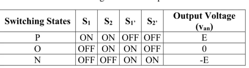
In each leg of a 3L-NPC, three switching state occurs as shown in Table 1-1. Table 1.1 Switching States of one phase of a 3L-NPC
Switching States S1 S2 S1’ S2’ Output Voltage (v an)
P ON ON OFF OFF E
O OFF ON ON OFF 0
N OFF OFF ON ON -E
Taking into account all three phases of the inverter, there will be 27 possible combinations of switching states. Based on the voltage vectors magnitude, they can be divided into four categories:
• Zero Vectors: contains three switching states that can be shown for three phases as {PPP}, {NNN} and {000} which produce zero voltage at the output;
• Small Vectors: some states that produce E/3 at the output; • Medium Vectors: whose magnitude is 3 E/3;
• Large Vectors: the magnitudes are 2E/3.
Sectors and Regions in SVM for 3L-NPC
As it can be seen in this figure, the reference voltage vector is shown by Vref which is located
in a region in each moment. Each sector and region is surrounded by switching vectors. So by calculating the time intervals of each state, the reference voltage can be produced by a combination of switching states.
In this method, the modulation index ma is defined as follows (Wu, 2006):
3 ref a d V m V =
Where Vd is the output phase voltage (E), and Vref is the reference voltage magnitude. Since
in a 3L-NPC the maximum Vref is the radius of the circle shown in Figure 1.23 which is 3
Vd/3, so the ma-max equals to 1.
Many developments have been performed on this method (Franquelo et al., 2008) which is flexible to be combined with evolutionary algorithms for optimized switching sequence (Cecati, Ciancetta et Siano, 2010).
37
1.3.3 DC Voltage Balancing
Using a DC capacitor in multilevel inverter makes the voltage balancing inevitable. Such inverters include NPC, FC and PUC. Using a PI controller is a simple method to control the capacitor voltage while there are many proposed methods to balance the voltage (Barros, Silva et Jesus, 2013; Hornik et Zhong, 2013; Marchesoni et Tenca, 2002; Ounejjar, Al-Haddad et Dessaint, 2012; Sano et Fujita, 2008; Shukla, Ghosh et Joshi, 2008; Xia et al., 2011). For instance, if the levels of a NPC increase, the number of DC capacitor used in DC link raises. Therefore, the voltages of each capacitor and the middle points should be balanced to reach a smooth waveform for output voltage. Most of voltage balancing techniques are based on control methods such as PI, predictive model, fuzzy and etc. as well, using auxiliary circuit to make additional path for capacitors currents has been reported that facilitate the energy exchanging of the capacitors to keep their voltages balanced (Shu et al., 2013).
One interesting feature of multilevel inverters is the fact that they usually have some redundant switching states which generate same voltage level using different current paths. Therefore, they would be the most helpful items in balancing capacitors voltages without requiring external controllers. Such voltage balancing techniques could decouple the voltage/current control in various applications.
All in all, the voltage balancing of the DC capacitors of a multilevel inverter is matter of importance especially in rectifiers or power system interface applications like active filters or STATCOM where a grid connected converter is needed.
1.4 Modeling and Control of Multilevel Inverter
Modeling of a multilevel inverter is the main step to design a proper controller to regulate the voltage or current. The first try on modeling a converter was done on an imbricated multilevel inverter in 1997 (Meynard, Fadel et Aouda, 1997). This model was derived based on the study of the harmonic equivalent circuit.
Some other works have been performed to model the multilevel inverters but there are a few papers totally, therefore it would be a challenging field for modeling various topologies with different methods such as average model, state space or small signal. For example, a CHB used as a STATCOM has been modeled based on small signal method to design a proper control strategy in balancing the DC voltages (Liu et al., 2009). The average model of the PUC inverter has been also derived in (Ounejjar, Al-Haddad et Grégoire, 2011) that helped to implement an appropriate controller of the DC capacitor voltage. A mathematical modelling of multilevel inverter is also introduced in (Ben Smida et Ben Ammar, 2010).
Multilevel inverters use many DC sources to produce higher voltage levels; therefore, their control becomes more complex. Since most of the multilevel inverters have isolated DC sources, they just need switching methods to produce desired voltage levels at the output. However, some topologies have capacitors as DC link which need voltage balancing control methods like PI controller to fix the DC voltage. Moreover, an associated controller is required for each application of the multilevel converters such as drive, charger, UPS, active filter and PV inverter.
1.5 State of The Art (Impact on Industry) and Originality of the research
In addition to the above-mentioned topologies there are some types of multilevel inverters that have been reported but they were not considered and developed in the market. Among the mentioned topologies, the CHB and NPC are still the most popular and accepted ones in industries, however there are some drawbacks associated with them. The other ones have some issues like high switching frequency, complex switching methods, difficult cooling system, large number of semiconductors, or using too many capacitors that needs a lot of isolators and makes the voltage balancing difficult. Note that the medium-voltage and high-power range in industries are 2.3-6.6 kV and 1-50 MW, respectively. And the desired switching frequency in industry is 500-700 Hz. In continue, some advantages and disadvantages of two most widely used types of multilevel inverters (NPC and CHB) are listed as the following (Kouro et al., 2010):
39
• NPC uses medium and high voltage components (IGCT, IGBT), whereas CHB employs solely low-voltage ones (LV-IGBT). Although CHB uses LV switches, it reaches higher voltage and power levels than NPC;
• NPC is definitely more proper for back-to-back applications than CHB which needs too many switches for this aim;
• NPC has simpler structure system and has flexibility for implementing various switching methods (PWM, SVM and etc.) on it;
• CHB needs a phase-shifting transformer usually to conform a 36-pulse rectifier system which is more expensive but improves input power quality.
Regarding all mentioned advantages and disadvantages of proposed topologies for multilevel inverters, there is still a lot of challenging on improving drawbacks in many aspects like topologies with less switching devices, less DC supplies, easier and faster voltage control, reducing the switching frequency and power losses, diminishing output harmonics, designing suitable output filters. The power electronics converters are widely used in industries and power networks which are so attractive for researchers to improve the performance, and with multilevel topologies the new era of such converters arrived. The growing applications of multilevel inverters show its increasing popularity and acceptable usage in market (industries and power systems).
Besides the provided information, some of the applications of multilevel converters with commercialized topologies are as the following that shows the state of the art of this technology (Leopoldo G. Franquelo, 2012; Wu, 2006):
Figure 1.24 illustrates a 4.16 kV and 1.2 MW drive which is manufactured by ABB and composed of 3L-NPC (right cabinet), cooling system and rectifier (middle cabinet) and controller (left cabinet).
GCT-based 3L-NPC drive by ABB (ACS1000)
Figure 1.25 shows a 4.16 kV and 7.5 MW drive designed and built by ASI Robicon by 11L-CHB. The phase shifting transformer (installed in left cabinet) supplies a 30-pulse rectifier.
41
ABB and Converteam have commercialized 3L-NPC back-to-back for wind power applications as shown in figures 1-26 and 1-27, respectively.
3L-NPC for wind power conversion by ABB (PCS-6000-wind)
3L-NPC for wind power conversion by Converteam (MV7000)
Figure 1.28 is a MMC for HVDC transmission system commercialized by SIEMENS. The power rating of this inverter is 1000 MW and the output frequency is 50-60 Hz.
MMC for HVDC with its Control System and Cooling System
1.6 Conclusion
multilevel converters are widely used for mining applications as regenerative conveyor, medical purposes like MRI gradient coil driver, hydro pump storage, STATCOM and Active Filters, FACTS, distributed generation, ship propulsion, train traction, aerospace and renewable energy (wind and photovoltaic) conversion (Alepuz et al., 2006; Biagini et al., 2011; Daher, Schmid et Antunes, 2008; Dixon et al., 2010; Kouro et al., 2010; Leopoldo G. Franquelo, 2012; Liu et Luo, 2005; Liu et al., 2009; Samuel, Gupta et Chandra, 2011; Xia et al., 2011). Most of the constructed multilevel inverters in industries have been devoted to the high power applications due to their good performance in very low switching frequency and using medium voltage switches. However, the google little box challenge, held in 2014, revealed the promising fact that such class of converters could be used in all range of power electronics converters due to reduced price of semiconductor switches. Since they can produce very low harmonic waveforms inherently, the size of the package would be small because of reduced size of the output passive filters. Having a single-dc-source option and less number of switches would be the most challenging part of this field.