HAL Id: hal-00077477
https://hal.archives-ouvertes.fr/hal-00077477
Submitted on 30 May 2006
HAL is a multi-disciplinary open access
archive for the deposit and dissemination of
sci-entific research documents, whether they are
pub-lished or not. The documents may come from
teaching and research institutions in France or
abroad, or from public or private research centers.
L’archive ouverte pluridisciplinaire HAL, est
destinée au dépôt et à la diffusion de documents
scientifiques de niveau recherche, publiés ou non,
émanant des établissements d’enseignement et de
recherche français ou étrangers, des laboratoires
publics ou privés.
Quartz Crystal Oscillator Classification by Dipolar
Analysis
Rémi Brendel, Farid Chirouf, Daniel Gillet, Nicolas Ratier, Franck
Lardet-Vieudrin, Mahmoud Addouche, Jérôme Delporte
To cite this version:
Rémi Brendel, Farid Chirouf, Daniel Gillet, Nicolas Ratier, Franck Lardet-Vieudrin, et al.. Quartz
Crystal Oscillator Classification by Dipolar Analysis. Proceedings of the Conference on Precision
Oscillations in Electronics and Optics (CAOL–POEO’2003), 2003, Alushta, Ukraine. pp.233-243.
�hal-00077477�
QUARTZ CRYSTAL OSCILLATOR CLASSIFICATION
BY DIPOLAR ANALYSIS
R. Brendel
1, F. Chirouf
1, D. Gillet
1, N. Ratier
1, F. Lardet-Vieudrin
1, M. Addouche
2, J. Delporte
31
Laboratoire de Physique et Métrologie des Oscillateurs du CNRS associé à l’Université de Franche-Comté 32, Avenue de l’Observatoire – 25044 Besançon Cedex – France
2Laboratoire d’Astrophysique de l’Observatoire de Besançon 41, Avenue de l’Observatoire – 25030 Besançon Cedex – France
3Centre National d’Études Spatiales 18, Avenue E. Belin – 31055 Toulouse Cedex – France
Abstract – The dipolar method associated with a nonlinear time domain simulation program make up a powerful tool to analyze high Q-factor circuits like quartz crystal oscillators. After a brief remainder of the dipolar method, the paper will attempt to identify the main amplifier characteristics such as limitation mechanism, input and output impedances, etc. and to point out their influence on the amplifier dipolar impedance. The effect of the amplifier nonlinearities on the oscillator cha-racteristics, as well as the particular role of the crystal parallel capacitance are particularly emphasized.
Keywords – Oscillators, modeling, dipolar method
I. INTRODUCTION
The dipolar analysis is a non-linear time domain method well suited to describe the behavior of high Q-factor crystal oscillators [1-3]. In this method, to overcome the unaccepta-bly long transient time needed to reach the steady state of high-Q circuits, the oscillator amplifier is separated from the resonator and replaced by a sinusoidal current source. The amplifier then behaves like a dipole the impedance of which is evaluated at the resonator frequency. An electrical simula-tion program like SPICE is used to perform a set of transient analyses of higher and higher amplitude so as to obtain the variation of both the dipolar resistance and reactance as a function of the current source amplitude.
When such a dipole is connected to a crystal resonator, oscillation occurs when the non-linear dipolar impedance is equal and opposite to the resonator impedance [4-5]. This leads to a non-linear equation that can be used to obtain the oscillation start-up condition, the steady state current ampli-tude and oscillation frequency or a time domain non-linear differential equation whose solution is the oscillation loop current. Because of the high resonator Q-factor, the oscilla-tion loop current is almost perfectly sinusoidal so that asymptotic method, like slowly varying functions method [6-7] can be used to obtain both amplitude and frequency transients without having to solve the initial nonlinear diffe-rential equation. The effect of noise can also be calculated by using a perturbation method in the vicinity of the steady state [8], and for noise Fourier components close to the car-rier, perturbation results in both amplitude and frequency modulation from which amplitude and phase noise spectra are easily calculated.
An implementation of the dipolar method achieved in the ADOQ program (“Analyse Dipolaire des Oscillateurs à Quartz”) is able to compute the steady state features of the oscillator: oscillation frequency, amplitude, drive level, sig-nal shape and gives the start-up condition for oscillation to occur [2]. Also the program performs accurate oscillator sensitivity calculation to various parameters (component value, supply voltage, etc.) as well as amplitude and phase noise spectra [8].
II. SIMULATION PRINCIPLE
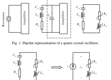
The nonlinear dipolar method consists in representing an oscillator by the quartz motional branch connected across a non-linear dipole amplifier (Fig. 1). The parallel capacit-ance and, if needed, the pulling capacitcapacit-ance, are included in the amplifier dipole. The impedance of the nonlinear dipole amplifier strongly depends on the current amplitude and weakly depends on the current frequency. It can be represented by a nonlinear resistance in series with a nonli-near reactance, symbolized for convenience in Fig. 1 by an inductance, that vary with the amplitude of the current.
Cq Lq Rq Ld Rd R e s o n a to r A m p li fi e r A m p li fi e r Cp Cq Lq Rq
Fig. 1. Dipolar representation of a quartz crystal oscillator.
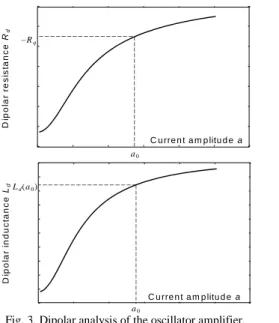
Ld Rd Cq Lq Rq Ld Rd i + vd –
Fig. 2. Dipolar analysis of the oscillator amplifier.
Because of the resonator’s high quality factor, the loop current in the oscillator is almost perfectly sinusoidal. Thus, the nonlinear behavior of the dipolar amplifier can be
ob-tained by replacing the resonator motional branch by a sinu-soidal current source, and performing a set of transient ana-lyses with increasing amplitudes by using an electrical simu-lator like SPICE (Fig. 2).
The complex impedance of the nonlinear dipole am-plifier is obtained, for each current amplitude value by per-forming a Fourier analysis on the steady state voltage across the dipole. Nonlinear amplifier resistance and reactance are obtained by giving the sinusoidal current a larger and larger amplitude (Fig. 3). a0 D ip o la r re s is ta n c e R d C u rre n t a m p litu d e a –Rq Ld(a0) a0 D ip o la r in d u c ta n c e L d C u rre n t a m p litu d e a
Fig. 3. Dipolar analysis of the oscillator amplifier.
The nonlinear differential equation of the oscillator is given by (1), where q is the quartz series resonant
frequen-cy and a is the amplitude of the current fundamental com-ponent i(t). In quartz crystal oscillator Lq Ld so that:
1
( )
2 1 ( ) 0 2 2 i L a L dt di a R R L dt i d q d q d q q (1) q q q L C 1 2 (2)The solution of this equation is taken under the form shown in (3) where a(t) and (t) are slowly varying func-tions of time.
i a(t) cos
qt (t)
(3) At low current amplitude level, the damping term of (1) should have a negative value to insure increasing amplitude solution. If Rds is the value of the nonlinear dipolarresis-tance at very low current amplitude, the start-up condition takes the form (4).
Rq Rds 0 (4)
As the oscillation amplitude increases, the dipolar resis-tance increases so that the value of the damping term in-creases. The steady state amplitude a0 is reached when this term becomes zero as given by (5) and Fig. 3.
Rq Rd(a0) 0 (5) q d q L a L ( ) 1 0 2 2 0 (6)
The steady state frequency is then given by (6) where
Ld(a0) is the value of the steady state dipolar inductance de-duced from the curve in Fig. 3.
III. OSCILLATOR AMPLIFIER CLASSIFICATIONS
A large number of amplifier circuits can be used to build an oscillator each having its own advantages and drawbacks. The choice among the different circuits is of course dictated by the application the oscillator will be used in, and also by technical considerations such as: frequency range, output power range, frequency stability, output wave-form, phase noise, etc. [9]. Even for a given set of specifica-tions there are many different circuits able to meet them and a particular choice is often a matter of personal or collective experience or skill rather than the conclusion of a methodi-cal analysis. It is not our claim to give a methodimethodi-cal reason-ing leadreason-ing to an optimal circuit, but more modestly, to give the designer an efficient tool to help him to make a good choice. u1 – + ZQ A m p Z1 vd – + i u2 – + Z2 Z3
Fig. 4. Amplifier representation.
u1 – + ZQ Z ’1 vd – + i u2 – + Z ’2 Z3 G ·u1 G 0 u1 – + ZQ Z ’1 vd – + i u2 – + Z ’2 Z3 A ·u1 R0 + – (a ) (b )
Fig. 5. Controlled current or voltage source representation of the amplifier with current (a) or voltage (b) controlled source.
u1 – + Z1 vd – + u2 – + Z2 G ·u1 ZQ i
Fig. 6. Reduced amplifier representation.
From the dipolar point of view, the amplifiers used in the oscillator circuits can be classified according several ways described in the following sections. So as to explain the classification method, the black box amplifier shown in Fig. 1 will be taken under the form shown in Fig. 4 where Z1 and Z2 are the amplifier input and output impedances in
pa-rallel with possible external impedances, while Z3 mainly represents the effect of the resonator’s parallel capacitance considered as a part of the amplifier circuit as stated in sec-tion II in parallel with a possible biasing impedance. Al-though it is possible, in a linear small signal analysis, to in-clude Z3 into Z1 and Z2 by a simple circuit transformation, in some case it is wiser to keep it as a separate impedance be-cause of the particular role it plays in the dipolar impedance as it will be shown later.
The amplifier itself can be represented either by a vol-tage controlled current source (Fig. 5.a) or by an equivalent voltage controlled voltage source (Fig. 5.b). In the linear case, by a simple circuit transformation, either one of the two representations in Fig. 5 can be reduced to the form shown in Fig. 6. Note that in Figs. 4, 5, and 6, the voltage reference node is not necessarily the ground node.
A general expression of the small signal dipolar imped-ance is obtained by replacing the resonator in Fig. 6 by a current source of same frequency as shown in Fig. 7.
u1 – + Z1 vd – + u2 – + Z2 G ·u1 i
Fig. 7. Dipolar impedance characterization.
By expressing the dipolar voltage vd as a function of the
current i, it is simple to obtain the small signal dipolar im-pedance under the form (7). From the dipolar point of view, the transconductance G (or the voltage gain A) can be real or complex, linear or nonlinear moreover all variables of the right hand side in (7) might be function of the current ampli-tude a, so that the nonlinear dipolar impedance take the form (8).
Zds Z1 Z2 GZ1Z2 (7)
Zd Rd(a) jXd(a) (8)
IV. AMPLITUDE LIMITATION
It is well known that the oscillation amplitude is deter-mined by the nonlinear behavior of the amplifier. From this point of view, the amplifier circuits can be split into several categories such as: saturation or cutoff limitation, hard or soft limitation, symmetrical or non-symmetrical limitation, with possible combination of these various limitation me-chanisms.
A. Hard Saturation Limiting
In the simple behavioral oscillator circuit shown Fig. 8.a, the amplifier is an ideal circuit having a real input im-pedance R, and a linear real positive gain A limited by sym-metrical saturation as shown in Fig. 8.b. In this case, be-cause the amplifier is assumed ideal with a zero output im-pedance , it cannot be reduced to a transconductance am-plifier.
The nonlinear transfer function of the amplifier is de-termined by the conditions (9).
sat sat V u u u V u u u Au u u u u 2 0 1 2 0 1 1 2 0 1 0 (9) u1 – + A m p R u2 – + vd – + i In p u t v o lta g e (V ) –1 –0.5 0 0 .5 1 –0.5 –0.4 –0.3 –0.2 –0.1 0 0 .1 0 .2 0 .3 0 .4 0 .5 O u tp u t v o lt a g e ( V ) (a ) (b )
Fig. 8. Simple behavioral oscillator with saturation limiting.
Values used are: A = 4, R = 100 , Vsat = 1 V.
For small value of the current i, the dipolar impedance
Zds given by (10) shows that it is constant, real and negative
if the gain A is greater than the unity.
Zds Rds R(1 A) (10)
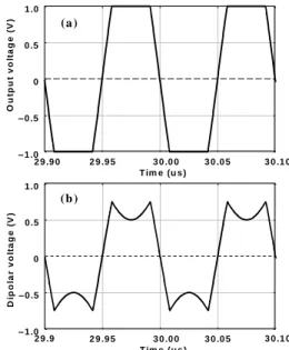
As the current amplitude a increases, the output voltage
u2 reaches the saturation level and becomes square shaped (Fig. 9.a) while the dipolar voltage vd becomes distorted
(Fig. 9.b). –1.0 –0.5 0 0 .5 1 .0 2 9 .9 0 2 9 .9 5 3 0 .0 0 3 0 .0 5 3 0 .1 0 O u tp u t v o lt a g e ( V ) T im e (u s ) (a ) –1.0 –0.5 0 0 .5 1 .0 2 9 .9 0 2 9 .9 5 3 0 .0 0 3 0 .0 5 3 0 .1 0 D ip o la r v o lt a g e ( V ) T im e (u s ) (b )
Fig. 9. Output and dipolar waveforms (hard saturation case).
–350 –300 –250 –200 –150 –100 –50 0 0 2 4 6 8 1 0 1 2 1 4 D ip o la r re s is ta n c e ( O h m s )
M o tio n a l C u rre n t A m p litu d e (m A )
By calculating the first harmonic of the dipolar voltage, it is possible to calculate the dipolar impedance as a function of the current amplitude a. In Fig. 10, it can be seen that the dipolar impedance Zd becomes nonlinear when the current
amplitude is larger than the limit aL given by (11).
AR V
aL sat (11)
In the present case, because there is no reactive part in the amplifier circuit, the dipolar impedance remains purely real so that Xd = 0. Moreover, according to the expression of Rds given by (10), it is obvious that an inverting amplifier
(A < 0) with real input and output impedances cannot be used in an oscillator circuit because Rd is always positive. B. Cutoff Limiting
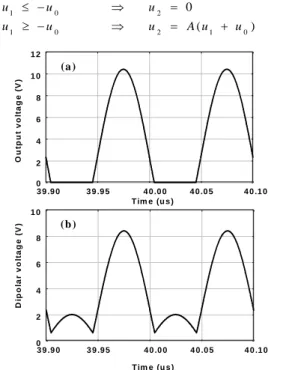
Another limiting mechanism often involved in the oscil-lator circuits is the cutoff limitation an example of which is shown Fig. 11. u1 – + A m p R u2 – + vd – + i (a ) (b ) 0 2 4 6 8 1 0 1 2 –2 –1.5 –1 –0.5 0 0 .5 1 1 .5 2 O u tp u t v o lt a g e (V ) In p u t v o lta g e (V )
Fig. 11. Simple behavioral oscillator with cutoff limiting.
Values used are: A = 4 , R = 100 , u0 = 0.6 V.
The oscillator shown has the same features as the pre-vious ones except that the nonlinear transfer function is now given by the conditions (12) and has the shape represented Fig. 11.b. ) ( 0 0 1 2 0 1 2 0 1 u u A u u u u u u (12) (a ) (b ) 0 2 4 6 8 1 0 3 9 .9 0 3 9 .9 5 4 0 .0 0 4 0 .0 5 4 0 .1 0 D ip o la r v o lt a g e ( V ) T im e (u s ) 0 2 4 6 8 1 0 1 2 3 9 .9 0 3 9 .9 5 4 0 .0 0 4 0 .0 5 4 0 .1 0 O u tp u t v o lt a g e ( V ) T im e (u s )
Fig. 12. Output and dipolar waveforms (cutoff case).
In this case, the output and dipolar voltages are no long-er symmetrical (Fig. 12). As in the saturation case, for small current amplitude, the dipolar impedance is given by (10) as long as the cutoff amplitude is not reached. For increasing current amplitude, the dipolar impedance increases as shown in Fig. 13, while the dipolar reactance remains null if there is no reactive part in the amplifier.
–350 –300 –250 –200 –150 –100 –50 0 0 1 0 2 0 3 0 4 0 5 0 6 0 7 0 8 0 9 0 1 0 0 M o tio n a l C u rre n t A m p litu d e (m A )
D ip o la r re s is ta n c e ( O h m s )
Fig. 13. Dipolar resistance (cutoff case). C. Soft Saturation Limiting
u1 – + A m p R u2 – + vd – + i (a) –15 –10 –5 0 5 1 0 1 5 –6 –4 –2 0 2 4 6 O u tp u t v o lt a g e ( V ) In p u t vo lta g e (V ) (b )
Fig. 14. Simple Van der Pol oscillator.
Values used are: A = 4, R = 100 , = 2 10–2 V–2.
(a ) (b ) –15 –10 – 5 0 5 1 0 1 5 4 9 .9 0 4 9 .9 5 5 0 .0 0 5 0 .0 5 5 0 .1 0 O u tp u t v o lt a g e ( V ) T im e (u s ) –8 –6 –4 –2 0 2 4 6 8 4 9 .9 0 4 9 .9 5 5 0 .0 0 5 0 .0 5 5 0 .1 0 D ip o la r v o lt a g e ( V ) T im e (u s )
Fig. 15. Output and dipolar waveforms (soft saturation case).
Let us examine now the case of a soft limiting mechan-ism. A simple example of such a circuit is given by the Van der Pol oscillator that has the same representation as the previous ones, but in this case the limitation due to the non-linear DC transfer function represented in Fig. 14.b is given by (13) where A is the small signal gain and is the
nonli-near coefficient (A and are assumed real and positive)
u2 Au1(1 u12) (13)
It is possible to show that in this case, the dipolar im-pedance can be derived under the form given by (14). 4 3 ) 1 ( 2 3 a R A R A Zd (14)
For small current amplitude, the dipolar impedance has the same expression (10) as in the two previous cases. As the current amplitude increases, the output and dipolar waveforms become distorted (Fig. 15), but, if there is no reactive part in the amplifier circuit, Zd remains real and
increases with amplitude according to the parabolic law (14) (Fig. 16). –3 5 0 –3 0 0 –2 5 0 –2 0 0 –1 5 0 –1 0 0 – 5 0 0 0 1 0 2 0 3 0 4 0 5 0 6 0 7 0 8 0 C u rre n t A m p litu d e (m A ) D ip o la r r e s is ta n c e ( O h m s )
Fig. 16. Dipolar resistance (soft saturation case).
V. FREQUENCY LIMITATION AND PARALLEL CAPACITANCE
The simple models presented so far are only ideal beha-vioral models without any reactive component. Any actual amplifier has a reactive part at least because they have a limited bandwidth or because of the parallel capacitance that is included in the amplifier part as pointed out in section II.
A. Amplifier Limited Bandwidth
– 350 – 300 – 250 – 200 – 150 – 100 –50 0 0 1 0 2 0 3 0 4 0 5 0 6 0 7 0 8 0 C u rre n t A m p litu d e (m A ) L im ite d b a n d w id th 0 5 1 0 1 5 2 0 2 5 3 0 3 5 4 0 4 5 5 0 0 1 0 2 0 3 0 4 0 5 0 6 0 7 0 8 0 C u rre n t A m p litu d e (m A ) L im ite d b a n d w id th D ip o la r r e s is ta n c e ( O h m s ) D ip o la r r e a c ta n c e ( O h m s )
Fig. 17. Dipolar impedance of a limited bandwidth amplifier. Oscillation frequency: 10 MHz, cutoff frequency: 100 MHz.
Assuming that the linear part of the amplifier gain A used in the previous cases in section IV has the form given by (15) where the cutoff frequency c is much larger than
the oscillation frequency, it is quite simple to demonstrate that in any case, the small signal dipolar impedance take the form (16) where it is obvious that the dipolar reactance is no longer null. 0 1 0 1 c c c j A A (15) 2 2 0 2 2 2 2 0 1 1 ) 1 ( c c ds c c ds RA X A R R (16)
When the amplifier has a limited bandwidth, it can be shown that the nonlinear part of the dipolar impedance does not depend strongly on the limiting mechanism, so it will be demonstrated only in the soft saturation case. Fig. 17 shows that the dipolar resistance remains practically unaffected while the dipolar reactance is now different from zero and decreases with the current amplitude.
B. Parallel Capacitance
As explained in section II, the parallel capacitance is in-cluded in the amplifier part of the oscillator circuit so that it can be considered in parallel with the dipolar impedance of the amplifier alone. Nevertheless, it is not so simple to ex-press the equivalent dipolar impedance of these two compo-nents associated in parallel because the voltage across the dipole is no longer linear.
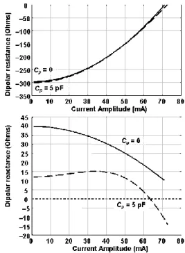
Fig. 18. Influence of the parallel capacitance on the dipolar impedance.
In Fig. 18 are compared the dipolar impedances of a li-mited bandwidth Van der Pol oscillator, as described in sec-tion IV C, with and without a parallel capacitance. As for the bandwidth effect, the dipolar resistance is practically not affected while the reactance exhibits a more important dis-tortion.
VI. INVERTING AMPLIFIER A. Representation u1 – + Z1 vd – + u2 – + Z2 G ·u1 i u1 – + R1 vd – + i u2 – + R2 G ·u1 C1 C2 (a ) (b )
Fig. 19. Inverting amplifier.
All the amplifier circuits presented so far had a positive gain with real input and output impedances so that, even at low frequency, they may have a negative dipolar resistance. This is the reason why an oscillator using such an amplifier type is often called “negative resistance oscillator.” Never-theless, most of the current crystal oscillators are using an inverting amplifier that can be represented as in Fig. 19.a, the small signal dipolar impedance of which is given by (17) where the transconductance G is real and positive.
Zds Z1 Z2 GZ1Z2 Rds jXds (17) Obviously, this expression may have a negative real part only if the input and output impedances Z1 and Z2 both have an imaginary part. A simple form of such a case is represented in Fig. 19.b where Z1 and Z2 are parallel combi-nations of a resistance and a capacitance.
B. Small Signal Analysis
The small signal dipolar impedance (17) can be ob-tained by replacing Z1 and Z2 by their expression (18), thus the real part Rds and imaginary part Xds of the small signal
dipolar impedance take the form (19) where 1 and 2 will be called the input and output time constant respectively.
2 2 2 2 2 2 2 2 1 1 1 2 1 2 1 1 1 1 C R R Z C R R Z (18) ) 1 )( 1 ( ) ( 1 1 ) 1 )( 1 ( ) 1 ( 1 1 2 2 2 2 1 2 2 1 2 1 2 2 2 2 2 2 1 2 1 1 2 2 2 2 1 2 2 1 2 2 1 2 2 2 2 2 1 2 1 R GR R R X R GR R R R ds ds (19) 1 2 2 1 C C G G c (20) 1 2 2 1 2 1 2 1 2 2 1 1 1 C C G R R G c (21)
By looking at the expression of Rds it should be
demon-strated that it can be negative only if two conditions are
ful-filled: the tranconductance G must be larger than the limit
Gc given by (20) and the frequency must be higher than the
limit c given by (21).
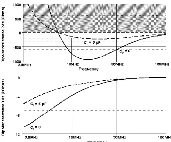
The small signal dipolar impedance for a given pair of impedances Z1 and Z2 is represented in Fig. 20 where oscil-lation cannot start if Rds is in the shaded area. Because Z1 and Z2 play symmetrical roles in the expression of the small signal dipolar impedance, the same curves are obtained when they are reversed.
Unlike the case of the non inverting amplifier with real input and output impedances, here the parallel capacitance strongly modify both the real and imaginary parts of the small signal dipolar impedance as shown in Fig. 20 where it can also be seen that the critical frequency c below which
the oscillation cannot start, is not affected by the parallel capacitance. In addition, as for the case where the parallel capacitance is null, the same small signal dipolar impedance is obtained when the input and output impedances are re-versed. It should be emphasized that the results presented so far in this section do not depend on the limiting mechanism but only on the small signal transconductance as well as the input and output impedance values.
Fig. 20. Small signal dipolar impedance of an inverting amplifier. G = 100 mA/V, C1 = C2 = 75 pF, R1 = 100 , R2 = 1000 .
C. Transconductance Amplifier with Cutoff Limiting
(a ) (b ) u1 – + Z1 vd – + i u2 – + Z2 iG 0 0 .2 0 .4 0 .6 0 .8 1 .0 –4 –2 0 2 4 6 8 1 0 O u tp u t c u r r e n t (A ) In p u t v o lta g e (V )
Fig. 21. Transconductance amplifier with cutoff limiting. G = 100 mA/V, u0 = 0.6 V.
Several simulations performed on transconductance amplifiers with different limitation mechanisms have shown that the input and output impedances (or time constants)
have similar effects on the nonlinear dipolar impedance. Thus, the attention will be focused only on the cutoff limit-ing mechanism often involved in the oscillator circuits. In this case, the nonlinear transconductance represented in Fig. 21.b is defined by the conditions (22).
) ( 0 0 1 0 1 0 1 u u G i u u i u u G G (22) (a ) –35 –30 –25 –20 –15 –10 –5 0 5 3 9 .8 8 3 9 .9 2 3 9 .9 6 4 0 .0 0 4 0 .0 4 4 0 .0 8 O u tp u t v o lt a g e ( V ) T im e (u s ) –35 –30 –25 –20 –15 –10 –5 0 5 3 9 .8 8 3 9 .9 2 3 9 .9 6 4 0 .0 0 4 0 .0 4 4 0 .0 8 D ip o la r v o lt a g e ( V ) T im e (u s ) (b )
Fig. 22. Output and dipolar waveforms (transconductance amplifier with cutoff limiting).
–2500 –2000 –1500 –500 0 –1000 –350 –300 –250 –200 –150 –100 –50 0 0 1 0 2 0 3 0 4 0 5 0 6 0 7 0 8 0 9 0 1 0 0 C u rre n t A m p litu d e (m A ) Cp = 0 Cp = 5 p F C u rre n t A m p litu d e (m A )
S o lid line s : inp ut Z1, o utp ut Z2
D a s he d line s : inp ut Z2, o utp ut Z1
Cp = 5 p F
Cp = 0
S o lid line s : in p ut Z1, o utp ut Z2
D a s he d line s : inp ut Z2, o utp ut Z1
0 1 0 2 0 3 0 4 0 5 0 6 0 7 0 8 0 9 0 1 0 0 D ip o la r r e s is ta n c e ( O h m s ) D ip o la r r e a c ta n c e ( O h m s )
Fig. 23. Dipolar impedance of a transconductance amplifier.
Z1: R1 = 100 // C1 = 75 pF, Z2: R2 = 1000 // C2 = 75 pF.
The output and dipolar waveforms of the transconduc-tance amplifier with cutoff limiting for a given pair of im-pedances Z1 and Z2 are shown in Fig. 22, and its dipolar im-pedance is represented in Fig. 23. Note that the dipolar resis-tance looks like the one of a non inverting amplifier having the same limiting mechanism (Fig. 13) but with a much larger reactance value. As demonstrated in section VI B, when the two impedances Z1 and Z2 are reversed, the dipolar
resistance and reactance keep the same value for small cur-rent amplitude but, as the amplitude increases, the two curves may have a quite different location. As for the small dipolar impedance, the parallel capacitance strongly modify both the dipolar resistance and reactance of the amplifier (Fig. 23). By looking at (6) it is obvious that a negative reac-tance corresponds to a positive frequency shift that can be-come very large if the resonator motional inductance Lq is
not much greater than the dipolar inductance Ld. In such a
case, the oscillation frequency may be close to the resonator antiresonant frequency, this is the reason why these tors are often improperly called “parallel resonance oscilla-tors.”
D. Input and Output Impedances
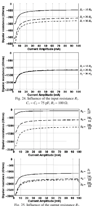
Fig. 24. Influence of the input resistance R1.
C1 = C2 = 75 pF, R2 = 100 .
Fig. 25. Influence of the output resistance R2.
Erreur ! Liaison incorrecte.
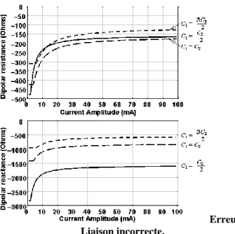
Fig. 26. Influence of the input capacitance C1.
R1 = 1000 , R2 = 100 , C2 = 100 pF.
Figures 24 to 27 show how the dipolar impedance of the transconductance amplifier previously used is modified when one of the four components defining the input and output impedances Z1 and Z2 is modified, the three others being kept constant. Of course, these figures do not cover all the possible combinations but only demonstrate how it is possible to use the dipolar method to optimize a circuit. It is obvious in Figs. 24 and 25, for example, that modifying the input or output resistance R1 or R2 drastically changes the dipolar resistance and therefore the motional current ampli-tude in the crystal, while the frequency shift due to the dipo-lar reactance is more sensitive to a change in the output re-sistance than in the input rere-sistance.
On the other hand, the dipolar resistance appears more sensitive to a change in the output capacitance than in the input capacitance, while both have an important effect in the dipolar reactance as shown in Figs. 26 and 27.
VII. CONCLUSION
In this work, the most important amplifier parameters that play a part in the behavior of quartz crystal oscillators have been studied by using the nonlinear dipolar that is a powerful and well suited method to analyze the characteris-tics and performance of high Q-factor circuits. The dipolar analysis has been successfully implemented in a dedicated software (ADOQ) whose efficiency and accuracy have been checked experimentally [10]. In addition to the main fea-tures described in the introduction, the program is currently being completed by a optimization module intended to help the designer in choosing the right circuit for a given purpose or to choose the right components for a given design.
Fig. 27. Influence of the output capacitance C2.
R1 = 1000 , R2 = 100 , C1 = 50 pF.
REFERENCES
[1] R. Brendel, D. Gillet, N. Ratier, F. Lardet-Vieudrin, and J. Delporte,
“Nonlinear dipolar modeling of quartz oscillators,” Proc. of the 14th
EFTF, Torino, Italy, pp. 184-188, March 2000.
[2] M. Addouche, R. Brendel, D. Gillet, N. Ratier, F. Lardet-Vieudrin,
and J. Delporte, “Modeling of quartz crystal oscillators by using non-linear dipolar method,” IEEE Trans. UFFC, vol. 50, pp. 487-495, May 2003.
[3] M. Addouche, N. Ratier, D. Gillet, R. Brendel, F. Lardet-Vieudrin,
and J. Delporte, “ADOQ: a quartz crystal oscillator simulation
soft-ware,” Proc. of the 55th IEEE IFCS, Seattle, USA, pp. 753-757, June
2001.
[4] K. Kurokawa, “Some basic characteristics of broadband negative
resistance oscillator circuits,” Bell System Technical Journal, pp. 1937-1955, July–August 1969.
[5] E.A. Vittoz, “Quartz oscillators for watches,” Proc. of the 10th
Inter-national Congress of Chronometry, pp. 131-140, Geneva, Switzer-land, September 1979.
[6] N. Kryloff, and N.N. Bogoliuboff, Introduction to Nonlinear
Me-chanics, Princeton University Press, 1943.
[7] A.A. Andronov, A.A. Vitt, and S.E. Khaikin, Theory of Oscillators,
New York, Pergamon Press, 1966, pp. 585-613.
[8] R. Brendel, D. Gillet, N. Ratier, M. Addouche, and J. Delporte,
“Os-cillator noise simulation by using nonlinear dipolar method,” Proc. of the 15th EFTF, Neuchâtel, Switzerland, pp. 123-128, March 2001.
[9] B. Parzen, A. Ballato, Design of Crystal and other Harmonic
Oscil-lators, New York, Wiley Intersciences, 1983.
[10] M. Addouche, N. Ratier, D. Gillet, R. Brendel, and J. Delporte, “Ex-perimental validation of the nonlinear dipolar method,” Proc. of the 16th EFTF, St. Petersburg, Russia, March 2002.