HAL Id: hal-02290292
https://hal.archives-ouvertes.fr/hal-02290292
Submitted on 18 Sep 2019HAL is a multi-disciplinary open access archive for the deposit and dissemination of sci-entific research documents, whether they are pub-lished or not. The documents may come from teaching and research institutions in France or abroad, or from public or private research centers.
L’archive ouverte pluridisciplinaire HAL, est destinée au dépôt et à la diffusion de documents scientifiques de niveau recherche, publiés ou non, émanant des établissements d’enseignement et de recherche français ou étrangers, des laboratoires publics ou privés.
High efficiency planar frequency multiplier at millimeter
waves and quasi optical investigations for sub-millimeter
applications
Jean-Luc Le Bras, Alain Peden, J.L. Le Bras, Marc Le Goff, Benoît
Deschamps, François Le Pennec, Daniel Bourreau, Serge Toutain
To cite this version:
Jean-Luc Le Bras, Alain Peden, J.L. Le Bras, Marc Le Goff, Benoît Deschamps, et al.. High efficiency planar frequency multiplier at millimeter waves and quasi optical investigations for sub-millimeter ap-plications. 29th European Microwave Conference, 1999, Oct 1999, Munich, Germany. �hal-02290292�
HIGH EFFICIENCY PLANAR FREQUENCY MULTIPLIER AT MILLIMETRE
WA VES AND QUASI-OPTICAL INVESTIGATIONS
FOR (SUB) MILLIMETRE APPLICATIONS
J.L. Le Bras*, M. Le Goff*, B. Deschamps*, F. Le Pennec*, A. Péden*, D. Bourreau*
and S. Toutain**
*
LEST UMR CNRS n ° 6616 - ENST de Bretagne - BP 832 - 29285 BREST CEDEX E-mail : Daniel.Bourreau@enst-bretagne.fr - Tél : 332 98 00 13 14 - Fax : 332 98 00 13 43** !RESTE - La Chantrerie - rue Christian Pauc - BP 60601 - 44306 NANTES Cedex 03
Abstract - This paper presents the design and
measurement of a hybrid varactor frequency multiplier in the millimetre wave range and the first investigations on a quasi-optical frequency doubler. For the planar circuit, a multilayer technology was used for the synthesis of the source and load impedances of the varactor. The conversion tosses are about 12 dB at 62 GHz with an output power of
10.8 dBm.
The measurement test bench and results on passive circuits in quasi-optical technology are presented. A quasi-optical doubler has also been investigated and designed and the first results are presented.
1. INTRODUCTION
For sub-millimetre wave applications, like FIRST and SOFIA programs [I], local oscillators at very high frequencies (up to 1 THz) are required for heterodyne receivers. A solution for providing power with low phase noise at sub-millimetre waves associates a low frequency oscillator with one - or more - frequency multipliers. This high frequency oscillator must have sufficient power for efficient driving of the down converter. Waveguide techniques are still widely used for millimetre and sub-millimetre radiometers, but planar circuits (hybrid or MMIC) could allow the drawbacks of waveguide whisker contacted diode multipliers (losses, fragility· ... ) to be overcome. However, no tuning can be done on planar multipliers and accurate modelling of the circuit is required. Quasi-optical solutions could be an interesting choice in the near future.
Il. PLANAR CIRCUIT DESIGN
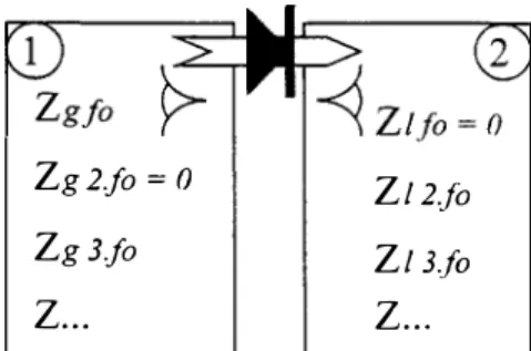
The source and load impedances and the working conditions of the multiplier are initialised with the Penfield and Rafuse equations [2]. Non-linear simulations are then used to optimise the results and
calculate the output power at fondamental and harmonie frequencies (figure 1 ).
Realisations at lower frequencies and sensitivity simulations give important information to control each step in the design procedure such as impedance terminations at fondamental and second harmonie frequencies (for a doubler). For the 28/56 GHz doubler, radial stubs are used to short-circuit the second harmonie at the input and the fondamental frequency at the output in a large frequency band. These stubs are positioned very close to the diode : this is very important to improve the conversion efficiency.
Classical planar technologies such as microstrip or coplanar technologies lead to very low and very high impedance transmission line sections for the diode matching, inducing high losses and then reducing the efficiency. A technology [3] with microstrip and multilayer coplanar lines (figure 2) was adopted to combine the advantages of each one. To obtain very low characteristic impedances, a small substrate thickness is used. But at the same time, high values are required. The multilayer technology detailed in figures 2 and 3 allows us to approximately retain the same central conductor width throughout the circuit, cutting the ground plane under the inductive transmission line sections. Classical coplanar lines are used at the accesses for coaxial probe measurements. The doubler circuit is fabricated on a 635 µm Alumina substrate with two metal layers and one dielectric layer. The surface is 6.7 mm x 9.7 mm.
Zg 2jo = 0 Zl 210
Zg Jjo Zl 3.fo
z...
z ...
Fig. 1. lmpedance optimization at each port. 29th European Microwave Conference - Munich 1999
Alumina suhstratc:
Fig. 2. Multilayer technology process on an Alumina substrate with two metal layers and one dielectric layer.
Fig. 3. Photograph of the multilayer frequency doubler. The surface is 6.7 mm x 9.7 mm.
III. RESUL TS FOR THE PLANAR DOUBLER Experimental results (figure 4) show that the optimal input frequency is 30.8 GHz for maximum output power (10.8 dBm) and efficiency (10.3 dB). The fondamental rejection is 25 dB. But at the 28.25 GHz input frequency, the fundamental rejection is optimal (-48 dB) as expected in simulations.
The electromagnetic simulation (2D and 3D) of the matching circuits was compared with HP-MDS library models used for the multiplier design. Differences in the computed S parameters, that is, the source and Joad impedances, can explain the frequency shift of the optimal output power. The dielectric permittivity of the thin layer should also be extracted for better accuracy.
No instabilities are observed at any frequency or power sweep. To have a good stability forecast many simulations and tests were performed.
1 51 JO 5 i !
01
-5 ! -10 j -15 -20 -25 -30 -+- Pout(@fO) • -•···· Pout(@2f0) P(dBm) -35 *"--'-�-'--ll--,..�--l��'--l-��-1-��-1 27 28 29 30 31 32Fig. 4. Output power at fondamental and second harmonie for Pin=20 dBm and V=-9 V.
IV. QUASI-OPTICAL TECHNIQUE
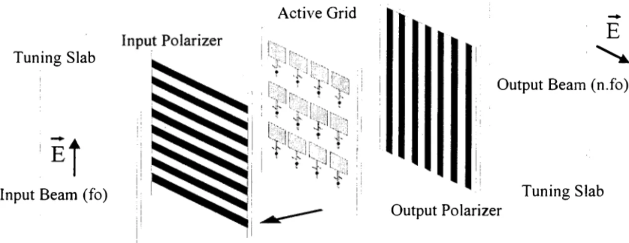
Recent developments give a solid state response for power capabilities at millimetre and sub-millimetre waves [4]. Fig. 5 illustrates an example of a quasi-optical circuit. Passive components were studied for accurate modelling [5]. The grid array can be an amplifier (output at fO) or a multiplier (output at n.fO).
Active planar arrays allow high level output power by recombination in free space with increased reliability. The matching of the active device (diode, transistor) can be done on the active grid, or can be carried out by extemal components such as a polarizer which works like a tuning short circuit and a dielectric slab like an adaptator. For a better input and output isolation, the electric fields at the two ports are cross-polarized. lt is also important for a multiplier to shunt the second harmonie at the input and the fundamental at the output with two separate circuits.
To design a millimetre doubler, the hybrid active grid of figures 6 and 7 with 69 cells, was chosen because of its simplicity ([ 4 J). The unit cell consists of two quarter wave dipole antennas in quadrature polarisation at the fundamental (38 GHz) and at the second harmonie (76 GHz). These antennas are connected via a V aractor diode which is the non-linear component. The active grid (i.e. the multiplier) is extemally matched with tuning slabs and polarizers which can be shifted during the measurement for optimal performances ( output power, conversion efficiency, ... ). The multiplier grid is printed on 210 µm substrate (i:;,=3.5).
Tuning Slab
Input Bearn ( fo)
Fig. 5. Quasi-optical frequency multiplier.
: ljl n!fll
191mm.,,mtfffi:&JepnJptl!f
f\l lJmwn
111 Ill'."10
11<. t2�·13""':'f:Ch 15 16 17ulimw11lu.itti11llmtktlMüudh11ilüd1wl,11ilüat1u1lt
···-t· . !
.
Fig. 6. Photograph of the active grid (dimension in cm).
Fig. 7. Detail of the diode connêcted tci dipole antennas.
•
Active Grid
-E
'--..
Output Bearn (n.fo)
Tuning Slab Output Polarizer
V. QUASI-OPTICAL MEASUREMENTS
A. Quasi-Optical test bench and modelling
For quasi-optical element characterisation and modelling, two test benches were carried out with Gaussian Optic Lens Antennas (GOLA) in the Ka band and in the W band. These benches were validated for S parameter measurements of passive quasi-optical elements such as polarizer, filter and dielectric slab. Simulated and measured S parameters show very good agreement. The complex permittivity of dielectric slabs is also extracted with high precision [7].
Using models or measured S parameters, simulations of simple quasi-optical fonctions (cascaded polarizer and slab for example) in classical CAD software (such as HP MDS) were carried out [5]. Non-linear simulations of the whole quasi-optical frequency multiplier were investigated and are still under study. The precise modelling of the component access through the antenna (dipole, ... ) is very important and rather difficult because it has to take into account ail the modes in the structure, the cross-polarisation and the multiple accesses (quasi optical and active components ).
B. Quasi-Optical multiplier measurement
With a Ka band GOLA, a W band GOLA and a Ka band power amplifier (lOW), the active array with input and output polarizers was tested with a 38 GHz input frequency.
In a first experiment, only 9 diodes were mounted on the array. But with so few diodes, the performances are not very attractive. The conversion efficiency is iess than -40d8 at the 76 GHz output frequency. To explain these poor results, it must be pointed out that the
1.
7 cm active area diameter with 9 diodes on the grid is too small in comparison with the 8 cm waist diameter of the inputGaussian beam. So, too little power is intercepted by the active area that is, by the 9 dipole antennas connected to the diodes. Most of the incident power is not transferred to the active device and the efficiency is very low.
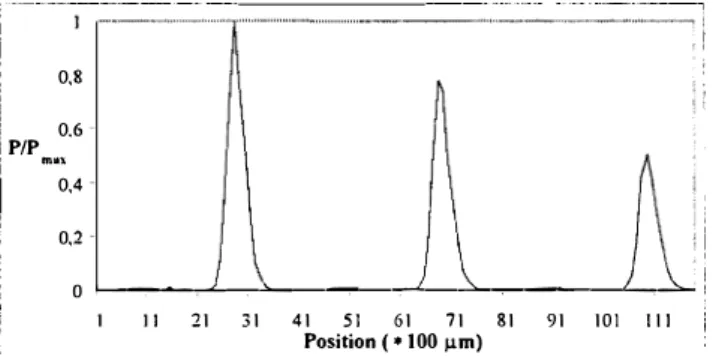
The second harmonie output power was measured for different positions of the input polarizer in relation to the active grid. Fig. 8 gives the normalised output power evolution and shows some periodicity. This result is very important because the positioning of the tuning elements must be very precise : there is only 700 µm between the maximal output power position and the minimal output power position. However, this behaviour was observed in preliminary non-linear simulations of the whole multiplier with very simple modelling (an inductance) of the dipole antenna.
VI. CONCLUSION
The design and measurement of a planar hybrid frequency doubler have been presented. The diode matching circuits make use of a coplanar and microstrip multilayer technology for high and low impedance synthesis without discontinuity of the central strip. With a 9.3 % (-10.3 dB) maximum conversion efficiency, it is a candidate for a state of the art of hybrid diode multipliers at this frequency. However, frequency shift was observed.
Quasi-optical technology is very attractive for combining solid state components, tuning circuits and power. Unlike passive circuits, the simulation of an active grid is quite difficult to achieve. Developments are in progress and a W band quasi-optical doubler will be tested in the near future.
ACKNOWLEDGEMENTS
The authors would like to thank Eric Rius (LEST Brest France) for his planar circuit design expertise.
0.8 0.6 P/P mo, 0.4 0 0 0 '----<---'---'---"---'----,� Il 21 31 41 51 61 71 81 91 101 Ill Position ( • 100 µm)
Fig. 8. Normalized output power measurement of the quasi-optical multiplier for ditlèrent positions of the input polarizer in relation to the active grid.
VII. REFERENCES
[l] N. Erickson, "THz Frequency Multiplier for FIRST and SOFIA", Proc. of the 2nd ESA Workshop on
Millimeter Wave Technology and Applications,
Espoo, pp. 423-428, May 1998
[2] P. Penfield and R.P. Rafuse, "Varactor Applications",
MIT Press, 1962.
[3] E. Rius et al., "lntegration of Various Types of Compensated Dielectric Bridges for Millimeter Coplanar Applications", IEEE MTT Symp. Digest, 1996.
[4] D. Steup, A.Simon, M. Shaalan, A. Grüb and C.I. Lin, "A Quasi-Optical Doubler-Array", !nt. Journal of
lnfrared and Millimetre Waves, Vol. 17, No 5, pp. 843-856, 1996
[5] J.L. Le Bras, M. Le Goff, B. Deschamps, A. Péden and D. Bourreau, "Quasi-Optical Circuit Measurement Method in the W Band", Proc. of the
2nd ESA Workshop on Millimeter Wave Technology and Applications, Espoo, pp. 453-457, May 1998 [6] S. Mons, R. Quéré, T. Peyretaillade, "Nonlinear
stability analysis of MMIC power amplifiers",
symposium EuMW"98, Amsterdam 5-9 october, vol 2,
pp 114-118, 1998
[7] M. Legoff, J.L. Le Bras, B. Deschamp, D. Rozuel, D. Bourreau, A. Péden, "Ka Band Quasi-Optical Test bench using Focusing Homs", EuMW'99, ta be