OATAO is an open access repository that collects the work of Toulouse
researchers and makes it freely available over the web where possible
Any correspondence concerning this service should be sent
to the repository administrator:
[email protected]
This is a Publisher’s version published in:
http://oatao.univ-toulouse.fr/23650
To cite this version:
Benchikhi, Mohamed
and El Ouatib, Rachida and Guillemet, Sophie
and
Er-Rakho, Lahcen and Durand, Bernard
Molten Salt Synthesis and
Characterization of CuIn(1-x)GaxS2 (x ≤0.3) Nanoparticles. (2015) Journal of
Chemical Sciences (Jchem), 2 (1). 21-25. ISSN 2339-5079
Molten Salt Synthesis and Characterization of
CuIn
(1-x)
Ga
x
S
2
(x ≤0.3) Nanoparticles
M. Benchikhi, R. El Ouatib, S. Guillemet-Fritsch, L. Er-Rakho, B. Durand
Abstract-Solid solutions CuIn(1-x)GaxS2 (x ≤ 0.3)were synthesized, with a yield of 70%, by reaction in molten KSCN at 400°C for 24h of CuCl2, InCl3 and GaCl3 with a ratio KSCN/Cu=15. The homogeneous solid solutions obtained are formed of nano-sized grains (70–100nm), with a specific surface area of 6.5 m2/g and a band gap between 1.5 and 1.8 eV.
Keywords-Chalcogenide, morphology, Semiconductor, Molten salt.
I. INTRODUCTION
Chalcopyrite compounds, of general formula Cu(In,Ga)(S,Se)2,have been studied extensively in
recent years [1-8] due to their applications as absorbers in solar cells[2-6], as well as for their use as photocatalysts [7]. These materials have a high absorption coefficient (greater than 104 cm-1) [8] and a
direct band gap from 1.04 (CuInSe2) to 2.43 eV
(CuGaS2) depending on their composition [9, 10].
Several studies have shown that the insertion of Ga in CuInSe2with contentbetween 25 and 35 molar %
allows obtaining the best photovoltaic efficiencies [5, 6]. Hanna et al [10] showed that the defect density in
CuIn(1-x)GaxSe2 is minimum at x = 0.3. Various reports
have shown that the physical properties of CuIn(S,Se)2
could be improved by doping [4,9-14].
Many studies have shown that the morphology and the particle size may significantly affect the intrinsic properties of CuInS2 [15-17]. Numerous
methods for the synthesis of Cu(In,Ga)(S,Se)2 have
been developed, such as laser removal [18], sputtering [14], co-evaporation [13], electrodeposition [19], sol-gel [20], spray pyrolysis[4,12], solvothermal [7] and organometallic routes [21]. Recently, Benchikhi et al. [1,22] proposed a process route to the fabrication of
ternary and quaternary chalcogenides by reaction in molten salts at 400°C.
In this paper, we report a simple method for the preparation of CuIn(1-x)GaxS2 nanoparticles by
reactions in molten salts. By analogy with CuIn (1-x)GaxSe2, which have a minimum defect concentration
at x= 0.3[10], we have limited the domain of solid solution at x =0.3.
II. EXPERIMENTAL
The solid solutions CuIn(1-x)GaxS2(x ≤0.3) were
synthesized by molten salts method using the following reactants: Copper chloride dihydrate CuCl2.2H2O
(Aldrich, 99.8 %), indium chloride InCl3 (Aldrich, 99.9
%) and gallium chloride GaCl3 (Aldrich, 99.9%).
Potassium thiocyanate KSCN (Prolabo) was used both as solvent and sulfurizating agent.
Figure 1 shows the schematic flow chart for the synthesis of CuIn(1-x)GaxS2(x ≤ 0.3) nanometric powders
by reaction in molten KSCN. The metal salts are mixed in the desired stoichiometric ratio and added to KSCN in the molar ratio SCN/Cu=15. The precursors were heat treated at 400 °C for 24 h under nitrogen flow in a vertical furnace. The heating and the cooling rates were stated at 2°C/min. After cooling at room temperature, the sulfides were extracted from the excess of salts by washings in deionized water, absolute ethanol and finally dried at 60°C for 12h. The reaction yield reached 70%.
The black powders obtained at the end of the process were characterized by X-ray diffraction (Brucker AXS D4, λCuKα = 0.15418 nm), by scanning (JEOLJSM 6400), and transmission (JEOL2010) electron microscopies, specific surface area
This work was supported by two French-Moroccan projects: Volubilis Partenariat Hubert Curien (PHC no. MA 09 205) and Projet de Recherches Convention Internationale du CNRS (CNRS-CNRST no w22572).
measurement (BET) (Micrometrics FlowsorbII2300), Raman(JobinYvon Labram HR 800) and UV-visible(UV-1601) spectroscopies.
Figure 1. Flowchart of the synthesis of CuIn(1-x)GaxS2(x ≤ 0.3) by
reaction in molten KSCN
III. RESULTS AND DISCUSSION
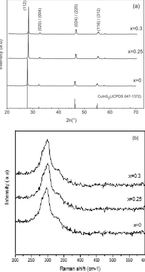
Structural characterization: The XRD patterns of the powders obtained at 400 °C for 24 h are given in figure 2-a. For the gallium contents lower than 0.3, all the peaks can be indexed to the chalcopyrite phase CuInS2 (JCPDS 047-1372), no impuritie can be
detected from this figure. The diffraction peaks shift slowly to the higher diffraction angle with increasing the gallium content. Lattice parameters (a and c) were determined for each composition by means of the Rietveld method.These lattice parameters decrease with the increase of Ga content (x) in the CuIn(1-x)GaxS2(x ≤
0.3) series (table1). This shows that the solid solution
CuIn(1-x)GaxS2 (x ≤ 0.3) is of substitution in which
indium atoms are substituted by smalleratoms of gallium.
TABLE1.LATTICE PARAMETERS AND BAND GAP (Eg)OFCuIn
(1-x)GaxS2(x≤ 0.3).
x= Ga/(Ga+In) a (nm) c (nm) c/a Eg (eV)
x=0 0.5521 1.1097 2.0099 1.51
x=0.25 0.5479 1.0941 1.9969 1.67
x=0.3 0.5461 1.0881 1.9925 1.78
In addition to the XRD, Raman investigation was performed to fully characterize the samples. The spectrum of CuInS2 (x=0) powder (figure 2-b) exhibits
a main peak close to 295 cm-1 and a shoulder close to
314-315 cm-1. These peaks are attributed to the
principal mode (A1) and secondary mode (B2/E)
observed in the chalcopyrite phase [1]. The frequency of the main peak (A1) increases with Ga-content; this result is in good agreement with the literature [23].
20 30 40 50 60 70 (a) (11 6) / ( 3 1 2 ) (02 4) / ( 22 0) (02 0) / ( 00 4) (11 2) Intensi ty (a.u) CuInS2(JCPDS 047-1372) x=0 x=0.25 x=0.3 2q(°)
Figure 2. Structural characterization: (a) RXD patterns and (b)
Raman spectra of CuIn(1-x)GaxS2powders.
Mechanism of formation: various reactional mechanisms have been proposed for the formation of the metallic sulfide in molten KSCN [1, 22,24]. This mechanism involves several steps:melting of KSCN and dissolution of metal salts, then the reduction of Cu2+ by SCN- via reaction (1) and lastly the thermal
decomposition of KSCN starting at 275°Cwith S and S2- formation via reactions (2) and (3)and the formation
of the chalcopyrite phase via reaction (4):
Cu2+ + 2 SCN-= Cu++ ½(CN)
2 + SCN- + S (1)
SCN- = CN- + S (2)
2CN- + S = S2- + (CN)
2 (3)
Washing and drying 400°C /24h
Reaction mixture
Black powder metal chloridesKSCN
CuIn(1-x)GaxS2 SCN/Cu=15Cu++(1-x)In3++xGa3+ +2S2-=CuIn
(1-x)GaxS2` (4)
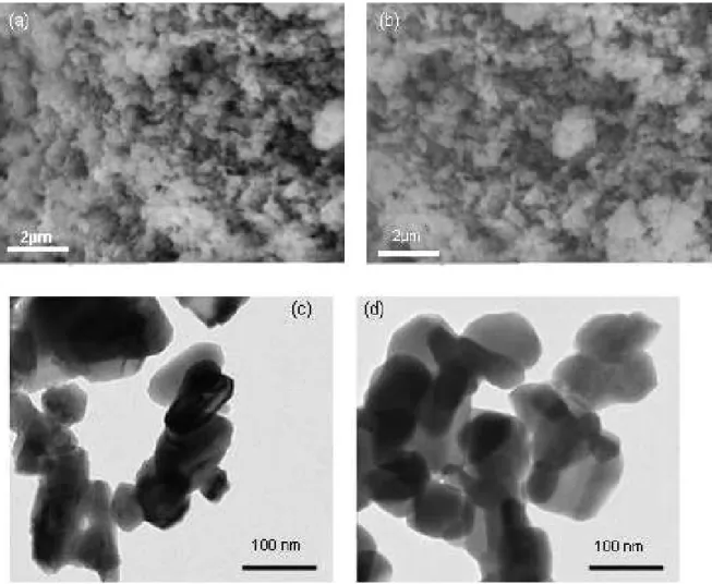
Morphological characterization: The influence of the Ga-content on the morphology of powders was evaluated. SEMobservation of the CuInS2 and
CuIn0,7Ga0.3S2 synthesized, by reaction in molten KSCN
at 400°C, (Figure 3) shows aggregated particles of
micronic size with a poly-disperse size distribution. Transmission electron microscopy (TEM) shows that these particles are constituted of nano-sized grains (70-100 nm) with more or less elongated shape (Figure3). Table 2 gives the average size of primary particles of each composition as well as their specific surface area.
Figure 3. Morphology: SEM micrographs of CuInS2 (a) and CuIn0,7Ga0,3S2 (b).TEM micrographs of CuInS2 (c) and CuIn0,7Ga0,3S2 (d).
Powders are constituted of relatively spherical particles.We calculated, from the specific surface area, the particle size (D) according the following equation (5):
D = 6 / (ρ S) (5) Whereρ is the densityand S the specific surface area. The determined values are given in table 2. According to these results, we can deduce that the Ga-content has no significant influence on the nanoparticles morphology.
TABLE2. SIZES OF PARTICLES OF CuIn(1-x)GaxS2(x=0 and x=0.3)
OBTAINED BY REACTION IN MOLTEN KSCN.
x=Ga/(Ga+In) Grain size MET (nm)
S (m2/g) Grain size
BET (nm)
x=0 80-100 6.0 205
x=0.3 70-100 6.5 195
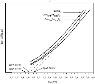
Measurement of the band gap Eg: The fundamental absorption (Eg) corresponds to the excitation of electrons from the valence band to the conduction band.
Optical absorption can be used to determine the optical band gap.
CuIn(1-x)GaxS2are direct band gap
materials[9,10].Their absorption coefficient (α) is related to the incident photon energy (hʋ) by the following equation (6) [25]:
(α hʋ) = A(hʋ –Eg)1/2(6)
Where A is a constant, Eg is the band gap and hʋ the energy of the incident photons (eV).The optical band gap Eg is determined by the intersection of the linear part of the curve (αhʋ)2 versus hʋ (Figure 4). The
values obtained show that Eg increases with the gallium content (table 1).This is in agreement with the previous experimental investigations[4,9].
Figure 4. Plot of (αhʋ)2 versus (hʋ) for CuIn
(1-x)GaxS2 (x≤ 0.3)
samples
IV. CONCLUSION
Solid solutions CuIn(1-x)GaxS2 (x ≤ 0.3) were
synthesized by reaction in a molten KSCN at 400°C for 24 h with the ratio KSCN/Cu=15. We have employed XRD, and Raman spectroscopy to confirm that the galliumis successfully incorporated into the chalcopyrite crystal structure (I-42d).The powders obtained are constituted of primary crystallites with sizes in the range 70–100 nm and exhibits a specific surface area close to 6.5 m2/g. The optical band gap has
increased from 1.51 to 1.79 eV with increasing Ga concentrations from 0 to 0.3.
REFERENCES
[1] M.Benchikhi, R. El Ouatib, S.Guillemet-Fritsch, J.Y.Chane-Ching, J.J.Demai, L.Er-Rakho, and B.Durand, “Synthesis of
CuInS2 nanometric powderbyreactioninmolten KSCN, ” Mater.
Lett., vol.136, pp.431-434, December 2014.
[2] Z.Hao, Y.Cui and G. Wang, “Colloidal synthesis of wurtzite
CuInS2 nanocrystals and their photovoltaic application,” Mater.
Lett., Vol.146, pp. 77-80, May 2015.
[3] M. Baneto, A. Enesca, C. Mihoreanu, Y. Lare, K. Jondo, K.Napo and A. Duta, “Effects of the growth temperature on the
properties of spray deposited CuInS2 thin films for photovoltaic
applications,” Ceram Int, Vol.41(3B), pp.4742-4749, April 2015.
[4] M.Ajili, M.Castagné and N. KamounTurki,
“CharacteristicsofCuIn1-xGaxS2 thin films
synthesizedbychemical spraypyrolysis,” Journal of
Luminescence, vol.150,pp. 1-7, January 2014.
[5] I. Repins, M. A. Contreras, B. Egaas, C. DeHart, J.Scharf , C. L
. Perkins, B. To, and R. Noufi,“19.9% efficient
ZnO/CdS/CuInGaSe2 solar cell with 81.2% fill factor,”
Prog. Photovolt.: Res. Appl.,vol.16(3), pp. 235-239, May 2008 [6] P. Jackson, D. Hariskos, E. Lotter, S. Paetel, R. Wuerz, R.
Menner, W. Wischmann, and M. Powalla, “New world record
efficiency for Cu(In,Ga)Se2 thin-film solar cells beyond 20%,”
Prog. Photovolt.: Res. Appl., vol.19(7), pp. 894-897, November 2011.
[7] C. Li, Z. Xi, W. Fang, M. Xing, and J. Zhang, “Enhanced
photocatalytic hydrogen evolution activity of CuInS2 loaded
TiO2 under solar light irradiation,”J. Solid State Chem., vol.
226, Pages 94-100, March 2015.
[8] H.M. Pathan, and C.D.Lokhande, “Chemical Deposition and Characterization of Copper Indium Disulphide Thin Films”, Appl. Surf. Sci., vol. 239, pp.11-18, 2004
[9] R.Kaigawa, A.Ohyama, T.Wada and R.Klenk, “Electrical
properties of homogeneous Cu(In,Ga)S2 films with varied
gallium content,” Thin Solid Films, vol. 515(15) pp.6260-6264, May 2007.
[10] G.Hanna, A.Jasenek, U.Rau, and H.W Schock, “Influence of
the Ga-content on the bulk defect densities
ofCu(In,Ga)Se2, Thin Solid Films, vol. 71, pp.371-373, 2001.
[11] N.Kamoun Allouche, N.Jebbari, C. Guasch, and N. Kamoun Turki, “Influence of aluminum doping in CuInS2 prepared by spray pyrolysis on different substrates,” J. Alloys. Compd., vol. 501(1), pp. 85-882, July 2010.
[12] C.Mahendran, and N.Suriyanarayanan, “Effect of Bi incorporation and temperature on the properties of sprayed
CuInS2 thin films,” Physica B: Condens Matter, vol. 408, pp.
62-67, January 2013.
[13] M. Ben Rabeh, M. Zribi, M. Kanzari, and B. Rezig, “Structural
and optical characterization of Sn incorporation in CuInS2 thin
films grown by vacuum evaporation method,” Mater. Lett,. vol. 59( 24),pp. 3164-3168,October 2005.
[14] M. Nie, and K. Elmer, “Growth and morphology of thin
Cu(In,Ga)S2 films during reactive magnetron co-sputtering,”
[15] S.Peng, J. Liang, L. Zhang, Y. Shi, and J. Chen, “Shape-controlled synthesis and optical characterization of chalcopyrite
CuInS2 microstructures,” J. Cryst. Growth, vol. 305 (1), pp.
99-103, July 2007.
[16] P.Guha, D. Das, A.B. Maity, D. Ganguli, and S. Chaudhuri,
“Synthesis of CuInS2 by chemical route: optical
characterization,” Sol. Energy Mater. Sol. Cells, vol. 80(1), pp.115-130, October 2003.
[17] P.Guha, S.Gorai, D. Ganguli, and
S.Chaudhuri,“Ammonia-mediated wet chemical synthesis of CuInS2,” Mater. Lett., vol.
57(12) , pp. 1786-1791, March 2003.
[18] A.K. Shuaibov, and M.P. Churchman, “The parameters of
Laser Plasmas Formed Using Polycrystalline CuInS2,Copper,
and indium Targets,” Technical Physics Lett., vol.29(6), pp.485-487, December 2003.
[19] J. Herrero, and J. Ortoga, “Electrodeposition of Cu-In alloys for preparing CuInS2 thin films,” Sol. Energy Mater., vol. 20 (1–2), pp. 53-65 , January1990.
[20] F.Aslan, M.Z. Zarbali, B.Yesilata, and J.H. Mutlu, “Effects of Cu/In ratio and annealing temperature on physical properties of dip-coated CuInS2 thin films,” Mater. Sci. Semicond. Process., vol.16(1), pp.138-142, February 2013.
[21] T.Kino, T.Kuzuya, K.Itoh, K.Sumiyama, T.Wakamatsu, and M.Ichidate, “Synthesis of Chacopyrite Nanoparticules via Thermal Decomposition of Metal- Thiolate,” Mater.Trans., vol.49 (3), pp.435-438, January 2008.
[22] M.Benchikhi, O. Zaberca, R.El Ouatib, B. Durand, F. Oftinger, A. Balocchi, and J.Y. Chane.Ching, “A high temperature route to the formation of highly pure quaternary chalcogenide particles, Mater. Lett., vol. 68(1), pp. 340-343, February 2012. [23] J. Zhong, W. Xiang, Y. Zhao, Q. Cai, Y. Wang, J. Wang, H.
Yang, and X. Liang, “Synthesis and characterization of
flower-like CuIn1−xGaxS2 (x = 0.3) microspheres,” Mater. Research
Bull.,vol. 47(3), pp. 861-866, March 2012.
[24] S. Collado, A. Laca, and M. Diaz, “Catalytic wet oxidation of thiocyanate with homogeneous copper(II) sulphate catalyst,”J. Hazardous Mater.,vol.177(1-3) pp. 183-189, May 2010. [25] N. Serpone , D. Lawless , and R. Khairutdinov, “Size Effects
on the Photophysical Properties of Colloidal Anatase TiO2 Particles: Size Quantization versus Direct Transitions in This Indirect Semiconductor” J. Phys. Chem, vol. 99, pp. 16646– 16654, November 1995.
AUTHORS’ PROFILE
Mohamed Benchikhi is a PhD student in Laboratoire de
Physico-Chimie des Matériaux Inorganiques, Faculté des Sciences Ain chock, Université Hassan II Casablanca, Maroc.
Dr. Rachida El Ouatib is a Professor in the Laboratoire de
Physico-Chimie des Matériaux Inorganiques, Faculté des Sciences Ain chock, Université Hassan II Casablanca, Maroc
Sophie_Guillemet-Fritsch is a Researcher Director in the
Institut Carnot CIRIMAT, CNRS Université de Toulouse, 118 route de Narbonne, 31062 Toulouse Cedex 9, France.
Dr. Lahcen Er-Rakho is a Professor in the Laboratoire de
Physico-Chimie des Matériaux Inorganiques, Faculté des Sciences Ain chock, Université Hassan II Casablanca, Maroc.
Dr. Bernard_Durand is a Professor in the Institut Carnot
CIRIMAT, CNRS Université de Toulouse, 118 route de Narbonne, 31062 Toulouse Cedex 9, France.