UNIVERSITÉ DE MONTRÉAL
ARCHITECTURAL ALTERNATIVES TO IMPLEMENT HIGH-PERFORMANCE ∆Σ MODULATORS
MOHAMMAD HONARPARVAR DÉPARTEMENT DE GÉNIE ÉLECTRIQUE ÉCOLE POLYTECHNIQUE DE MONTRÉAL
THÈSE PRÉSENTÉE EN VUE DE L’OBTENTION DU DIPLÔME DE PHILOSOPHIÆ DOCTOR
(GÉNIE ÉLECTRIQUE) AVRIL 2019
c
ÉCOLE POLYTECHNIQUE DE MONTRÉAL
Cette thèse intitulée :
ARCHITECTURAL ALTERNATIVES TO IMPLEMENT HIGH-PERFORMANCE ∆Σ MODULATORS
présentée par : HONARPARVAR Mohammad
en vue de l’obtention du diplôme de : Philosophiæ Doctor a été dûment acceptée par le jury d’examen constitué de :
M. SAVARIA Yvon, Ph. D., président
M. SAWAN Mohamad, Ph. D., membre et directeur de recherche M. AUDET Yves, Ph. D., membre
iii DEDICATION
To my Mother and Father, To Elham.
ACKNOWLEDGEMENTS
First and foremost I would like to express my profound gratitude to my supervisor, Professor Mohamad Sawan, for giving me the chance to pursue my graduate study and grow. He has given me an endless freedom to explore analog and mixed signal world. Very special thanks to Professor Jose M. de la Rosa for his kind comments and feedback during my study. I spent six months visiting scholar in his laboratory and it is an undeniable fact that it has been one of my best moments during my life. I hope I can keep collaborating with these two fantastic professors.
I also would like to thank my committee members Professor Yvon Savaria, Professor Yves Au-det and Professor Gordon W. Roberts for accepting to evaluate this thesis. It is an undeniable fact that their feedback will enrich the presented materials in the thesis.
I would like to thank all my friends in Polystim Neurotechnologies Laboratory, specially Ghazal Nabovati, Zied Koubaa, Mohammad Noghabaei, Fereidoon Hashemi, Leila Montazeri and Elie Bou Assi.
I am grateful to all the staff of Electrical Engineering Department of Polytechnique Montreal, specially Marie-Yannick Laplante and Réjean Lepage for all their support.
I am also grateful for the financial support from NSERC, ReSMiQ, and CMC Microsystems. Last but not least, I do not even know how to thank my mother and father for their uncondi-tional love and support. They have worked in so many ways to help me achieve my ambitious goals. I have to thank my wife, Elham, who has always been with me to support my endeavors represented here. She deserves very special words of acknowledgement and thanks.
v RÉSUMÉ
Le besoin d’appareils portatifs, de téléphones intelligents et de systèmes microélectroniques implantables médicaux s’accroît remarquablement. Cependant, l’optimisation de l’alimen-tation de tous ces appareils électroniques portables est l’un des principaux défis en raison du manque de piles à grande capacité utilisées pour les alimenter. C’est un fait bien établi que le convertisseur analogique-numérique (CAN) est l’un des blocs les plus critiques de ces appareils et qu’il doit convertir efficacement les signaux analogiques au monde numérique pour effectuer un post-traitement tel que l’extraction de caractéristiques. Parmi les différents types de CAN, les modulateurs Delta Sigma (∆ΣM) ont été utilisés dans ces appareils en raison des fonctionnalités alléchantes qu’ils offrent. En raison du suréchantillonnage et pour éloigner le bruit de la bande d’intérêt, un CAN haute résolution peut être obtenu avec les architectures ∆Σ. Il offre également un compromis entre la fréquence d’échantillonnage et la résolution, tout en offrant une architecture programmable pour réaliser un CAN flexible. Ces CAN peuvent être implémentés avec des blocs analogiques de faible précision. De plus, ils peuvent être efficacement optimisés au niveau de l’architecture et circuits correspondants. Cette dernière caractéristique a été une motivation pour proposer différentes architectures au fil des ans.
Cette thèse contribue à ce sujet en explorant de nouvelles architectures pour optimiser la structure ∆ΣM en termes de résolution, de consommation d’énergie et de surface de silicium. Des soucis particuliers doivent également être pris en compte pour faciliter la mise en œuvre du ∆ΣM. D’autre part, les nouveaux procédés CMOS de conception et fabrication apportent des améliorations remarquables en termes de vitesse, de taille et de consommation d’éner-gie lors de la mise en œuvre de circuits numériques. Une telle mise à l’échelle agressive des procédés, rend la conception de blocs analogiques tel que un amplificateur de transconduc-tance opérationnel (OTA), difficile. Par conséquent, des soins spéciaux sont également pris en compte dans cette thèse pour surmonter les problèmes énumérés.
Ayant mentionné ci-dessus que cette thèse est principalement composée de deux parties prin-cipales. La première concerne les nouvelles architectures implémentées en mode de tension et la seconde partie contient une nouvelle architecture réalisée en mode hybride tension et temps. Les CAN proposés sont implémentés en circuits à capacités commutées tout en pré-sentant une solution pour surmonter les limites citées précédemment. Un amplificateur à base d’onduleur est proposé pour réaliser les intégrateurs réquis pour construire un modulateur delta sigma (∆ΣM). On montre que l’OTA proposé est suffisamment robuste par rapport
Processus voltage et température (PVT). Pour la deuxième partie de la thèse, il est démon-tré que le mode hybride (tension et temps) est une approche bénéfique pour mettre en œuvre un ∆ΣM. Par conséquent, un oscillateur en anneau à temps continu basé sur l’architecture MASH ∆ΣM est ciblé pour la deuxième partie de la thèse. On montre que le budget de puis-sance du ∆ΣM est principalement limité par les OTA nécessaires à la réalisation du filtre de la rétroaction du circuit. Pour s’attaquer à ce problème, une partie de la conception est trans-férée dans le domaine temporel afin de tirer parti des avantages de la réduction de l’échelle technologique. De plus, la solution hybride proposée facilite l’implémentation du ∆ΣM.
vii ABSTRACT
The need for hand-held devices, smart-phones and medical implantable microelectronic sys-tems, is remarkably growing up. However, keeping all these electronic devices power opti-mized is one of the main challenges due to the lack of long life-time batteries utilized to power them up. It is a well-established fact that analog-to-digital converter (ADC) is one of the most critical building blocks of such devices and it needs to efficiently convert analog sig-nals to the digital world to perform post processing such as channelizing, feature extraction, etc. Among various type of ADCs, Delta Sigma Modulators (∆ΣMs) have been widely used in those devices due to the tempting features they offer. In fact, due to oversampling and noise-shaping technique a high-resolution ADC can be achieved with ∆Σ architectures. It also offers a compromise between sampling frequency and resolution while providing a highly-programmable approach to realize an ADC. Moreover, such ADCs can be implemented with low-precision analog blocks. Last but not the least, they are capable of being effectively power optimized at both architectural and circuit levels. The latter has been a motivation to proposed different architectures over the years.
This thesis contributes to this topic by exploring new architectures to effectively optimize the ∆ΣM structure in terms of resolution, power consumption and chip area. Special cares must also be taken into account to ease the implementation of the ∆ΣM. On the other hand, advanced node CMOS processes bring remarkable improvements in terms of speed, size and power consumption while implementing digital circuits. Such an aggressive process scaling, however, make the design of analog blocks, e.g. operational transconductance amplifiers (OTAs), cumbersome. Therefore, special cares are also taken into account in this thesis to overcome the mentioned issues.
Having had above mentioned discussion, this thesis is mainly split in two main categories. First category addresses new architectures implemented in a pure voltage domain and the second category contains new architecture realized in a hybrid voltage and time domain. In doing so, the thesis first focuses on a switched-capacitor implementation of a ∆ΣM while presenting an architectural solution to overcome the limitations of the previous approaches. This limitations include a power hungry adder in a conventional feed-forward topology as well as power hungry OTAs. An inverter-based amplifier is also proposed to realize the integrators of the switched-capacitor ∆ΣM. It is shown that the proposed OTA is robust enough over process, voltage and temperatures (PVTs). For the second part of the thesis, it is demonstrated that a hybrid voltage and time domain is an acceptable venue to implement
a ∆ΣM. Therefore, a continuous time gated ring oscillator based MASH ∆ΣM is targeted for the second part of the thesis. It is shown that the power budget of ∆ΣMs is mostly limited by the operational amplifiers required to realize the loop filter. To tackle this issue, part of the design is shifted to the time-domain to take the advantages of a scaling friendly environment. Moreover, the proposed hybrid solution eases the implementation of the ∆ΣM.
ix TABLE OF CONTENTS DEDICATION . . . iii ACKNOWLEDGEMENTS . . . iv RÉSUMÉ . . . v ABSTRACT . . . vii TABLE OF CONTENTS . . . ix
LIST OF TABLES . . . xii
LIST OF FIGURES . . . xiii
LIST OF ABBREVIATIONS . . . xvii
CHAPTER 1 INTRODUCTION . . . 1 1.1 Motivation . . . 1 1.2 Problems statement . . . 2 1.2.1 LBW ADCs limitations . . . 2 1.2.2 WBW ADCs limitations . . . 3 1.3 Research objectives . . . 5
1.3.1 LBW ADC research objectives . . . 5
1.3.2 WBW ADC research objectives . . . 6
1.4 General organization of the thesis . . . 7
CHAPTER 2 LITERATURE REVIEW . . . 8
2.1 Literature on LBW SC-∆ΣMs . . . 8
2.2 Literature on WBW ∆ΣMs . . . 9
2.2.1 ∆ΣMs with time-domain blocks . . . 9
2.3 Conclusion . . . 22
CHAPTER 3 ARTICLE 1 : A 0.9-V 100-µW FEEDFORWARD ADDER-LESS INVERTER-BASED MASH ∆Σ MODULATOR WITH 91-dB DYNAMIC RANGE AND 20-kHz BANDWIDTH . . . 23
3.2 Abstract . . . 23
3.3 Introduction . . . 24
3.4 Background on Feedback and Feedforward ∆ΣMs . . . 26
3.5 Proposed Adder-less MASH FF ∆ΣM . . . 28
3.5.1 Adder-less Single-stage Feedforward Architecture . . . 28
3.5.2 Proposed Adder-less MASH Feedforward Architecture . . . 30
3.6 High-level Synthesis . . . 32
3.6.1 Modulator Loop Filter Coefficients Scaling . . . 32
3.6.2 Sampling Capacitor of the Front-end Integrator . . . 35
3.6.3 OTA Specifications . . . 36
3.6.4 Jitter effect . . . 36
3.6.5 Capacitor Mismatch . . . 38
3.7 Circuit-Level Implementation . . . 39
3.7.1 Proposed Self and bulk Biased OTA . . . 40
3.7.2 Comparator . . . 49
3.8 Experimental results . . . 50
3.9 Conclusion . . . 54
CHAPTER 4 ARTICLE 2 : SMASH ∆Σ MODULATOR WITH ADDERLESS FEED-FORWARD LOOP FILTER . . . 55
4.1 Overview . . . 55
4.2 Abstract . . . 55
4.3 Introduction . . . 55
4.4 Proposed SMASH topology . . . 57
4.5 Simulation results . . . 58
4.6 Conclusion . . . 61
CHAPTER 5 ARTICLE 3 : A 10-MHz BW 79.2-dB SNDR 640-MS/s CONTINUOUS-TIME FOURTH-ORDER MASH ∆Σ MODULATOR USING GRO-BASED QUAN-TIZATION . . . 62
5.1 Overview . . . 62
5.2 Abstract . . . 62
5.3 Introduction . . . 63
5.4 Proposed Modulator Architecture . . . 66
5.4.1 Time-based Quantization Error Extraction and Generation . . . 68
5.4.2 Linear Analysis of the Modulator . . . 69
xi
5.5 Effect of Main Non-idealities . . . 72
5.5.1 Modulation depth and inter-modulation harmonics . . . 72
5.5.2 Mismatch of GROs’ Frequencies . . . 74
5.5.3 Phase Noise of GROs . . . 75
5.5.4 Supply voltage error . . . 76
5.5.5 Comparator delay . . . 76 5.5.6 Loop-filter non-idealities . . . 78 5.6 Circuit Implementation . . . 79 5.6.1 Operational Amplifiers . . . 80 5.6.2 Feedback DACs . . . 83 5.6.3 GRO-based Quantizer . . . 83 5.7 Measurement Results . . . 85 5.8 Conclusion . . . 88
CHAPTER 6 GENERAL DISCUSSION . . . 89
CHAPTER 7 CONCLUSION AND RECOMMENDATIONS . . . 93
7.1 Conclusion . . . 93
7.2 Research contributions . . . 94
7.3 Recommendations for future work . . . 95
7.4 Publication . . . 96
7.4.1 Journal publications . . . 96
7.4.2 Conference papers . . . 96
LIST OF TABLES
Table 1.1 Examples of existing and emerging applications for biomedical devices [1] 2 Table 3.1 Coefficients of the Proposed ∆ΣM after Scaling . . . 35 Table 3.2 High-Level Sizing of the Proposed ∆ΣM . . . 41 Table 3.3 Simulated Performance of the OTAs . . . 48 Table 3.4 Measured Performance and Comparison with State of the Art . . . . 53 Table 5.1 Performance Summary and Comparison with the State of the Art all
xiii
LIST OF FIGURES
Figure 1.1 Conceptual diagram of a generic biomedical device . . . 1 Figure 1.2 Block diagram of a smart sensor chip, [2] ( c [2005] IEEE) . . . 3 Figure 1.3 Figure of Merit (FOM) against SNDR for various ADC architectures[6,
7] ( c [2016] IEEE, c [2016] IEEE) . . . 4 Figure 1.4 FOM1 (F OM1 = 2EN OB(bit).output rate(S/s)P (W ) ) against BW for various types
of ∆ΣMs [10]( c [2018] John Wiley and Sons) . . . 5 Figure 2.1 Translation of voltage noise to timing noise[21] ( c [2011] IEEE) . . . 11 Figure 2.2 Basic single-shot TDC [21] ( c [2011] IEEE) . . . 11 Figure 2.3 (a) Conventional multi-bit delta sigma modulator.(b) Time-domain
quantizer/DAC based delta sigma modulator [21] ( c [2011] IEEE) . . 11 Figure 2.4 Simplified schematics of the TDC used as quantizer in a CT-DSM [21]
( c [2011] IEEE) . . . 12 Figure 2.5 Barrel shifting occurs through delay elements across different
measu-rements [30, 31] ( c [2008] IEEE, c [2009] IEEE) . . . 13 Figure 2.6 Two-step VCO-based delta sigma ADC architecture [32] ( c [2015] IEEE) 14 Figure 2.7 (a) Block diagram of a VCO-based 0-delta sigma MASH ADC, (b)
Signal model of the proposed MASH ADC [37] ( c [2015] IEEE) . . . 15 Figure 2.8 PWM-generator followed by VCO-based ADC [41] ( c [2011] IEEE) . 17 Figure 2.9 PWM-generator followed by VCO-based ADC [42] ( c [2012] IEEE) . 17 Figure 2.10 Gated ring oscillator TDC [25] ( c [2009] IEEE) . . . 18 Figure 2.11 GRO-based MASH 1-3 and its timing error feedback filter [50] ( c [2015]
IEEE) . . . 18 Figure 2.12 CT-∆ΣM with VCO-based quantizer [13, 30, 31] ( c [2012] IEEE, c [2008]
IEEE, c [2009] IEEE) . . . 19 Figure 2.13 Voltage-to-phase VCO-based ADC [31] ( c [2009] IEEE) . . . 20 Figure 2.14 PSD of (a) voltage-to-frequency VCO ADC [30], (b) voltage-to-phase
VCO ADC [31] ( c [2008] IEEE, c [2009] IEEE) . . . 21 Figure 2.15 Fourth order CT-∆ΣM with voltage-to-phase VCO-based ADC [31]
( c [2009] IEEE) . . . 21 Figure 2.16 Second order CT-∆ΣM with residue-cancelling VCO-based quantizer [13]
( c [2012] IEEE) . . . 22 Figure 3.1 Conventional ∆ΣM architectures (a) FB structure, (b) FF structure. 26 Figure 3.2 Adder-less FF ∆ΣM with single (multi)-bit quantizer. . . 29
Figure 3.3 Quantization error extraction : conventional method (red) and propo-sed method upropo-sed in the adder-less FF ∆ΣM (blue). . . 30 Figure 3.4 System-level diagram of the proposed adder-less MASH ∆ΣM. . . 32 Figure 3.5 Integrator output swing (normalized to the ∆ΣM full scale) versus
in-put signal level : (a) Single-bit modulator synthesized through an NTF of (1 − z−1)4 and before scaling, (b) Single-bit modulator through an
NTF of (1 − z−1)4 and after scaling, (c) 1.5-bit modulator synthesized
through an NTF of (1 − z−1)4 and before scaling, (d) 4-bit modulator
synthesized through an NTF of (1−z−1)4and before scaling, (e) Single-bit modulator synthesized through an NTF with an out-of-band gain of 1.5 (Hinf = 1.5) and before scaling, (f) Single-bit modulator
syn-thesized through an NTF with an out-of-band gain of 1.5 (Hinf = 1.5)
and after scaling. . . 33 Figure 3.6 Histogram of the integrator output swings relative to the FS voltage. 34 Figure 3.7 Maximum IBN versus integration capacitor size of the first integrator. 37 Figure 3.8 SQNR versus GBW and SR in the front-end OTA. . . 37 Figure 3.9 Maximum in-band noise versus OTA DC-gain. . . 38 Figure 3.10 SJNR versus input signal frequency and clock jitter standard deviation. 39 Figure 3.11 Monte Carlo simulation results by considering a capacitor-ratio
mis-match of : (a) 0.1%, (b) 0.2%, (c) 0.3% and (4) 0.4%. . . . 40 Figure 3.12 Schematic (single-ended) of the proposed adder-less MASH 2-2 ∆ΣM. 42 Figure 3.13 Inverter-based OTA, (a) Proposed SB inverter-based OTA in the weak
inversion, (b) Proposed SBB inverter-based OTA in the weak inversion, (c) CMFB circuit. . . 43 Figure 3.14 Simulated performance of the front-end SBB inverter-based OTA over
PVT variations : (a) DC-gain, (b) GBW and (c) static power. . . 46 Figure 3.15 Simulated step response of the first integrator (a) comparison of SB
and SBB inverter-based OTA for slow corner and (b) settling-time over PVT variations. . . 48 Figure 3.16 PSRR versus frequency. . . 49 Figure 3.17 CMRR versus frequency. . . 49 Figure 3.18 Latch-based comparator used to implement the 1-bit quantizer. . . . 50 Figure 3.19 (a) Chip micrograph and test board and (b) Measurement setup. . . 51 Figure 3.20 Spectrum of the modulator. . . 52 Figure 3.21 SNR, SNDR versus input signal level. . . 52 Figure 3.22 Power consumed by the different ∆ΣM building blocks. . . 54
xv
Figure 4.1 Block diagram of the conventional SMASH architecture [79] . . . 56
Figure 4.2 Block diagram of the modified SMASH [80] . . . 56
Figure 4.3 Block diagram of proposed adderless SMASH ∆ΣM . . . 58
Figure 4.4 SQNR versus OTA DC-gain . . . 59
Figure 4.5 SQNR versus input signal level . . . 59
Figure 4.6 First integrator output histogram . . . 60
Figure 4.7 Effect of OTA nonlinearity on the SNDR . . . 60
Figure 5.1 Conceptual block diagram of prior approaches to implement time/frequency-based quantizers in ∆ΣMs : Nyquist rate TDC [21], V-to-F VCOQ [30], V-to-P VCOQ [31] and RC-VCOQ [13]. . . 64
Figure 5.2 Conceptual block diagram of prior approaches to implement VCOQ in an open-loop mode : (a) Naturally sampled PWM followed by a VCOQ to digitize the input signal [41], (b) VCOQ to digitize quantization noise in the back-end of a multi-rate MASH ∆ΣM [53]. . . 65
Figure 5.3 Proposed GROQ-based CT MASH ∆ΣM : (a) block diagram, (b) DT representation of the GRO-TDC (left) and its equivalent linear model to synthesize the NTF (right) both showing an NTF of (1 − z−1) and a STF of unity, (c) Linear model of the proposed modulator. . . 67
Figure 5.4 (a) Chronogram of the estimation of quantization error, (b) Proposed quantization error extractor, QE-ext (ph : output phase of the GRO, p : PWM pulse, E : quantization error and n : number of GRO phases), (c) Quantization error extraction in CT MASH ∆ΣMs with voltage mode quantizer [96]-[97]. . . 69
Figure 5.5 Simulated PSD of the proposed ∆ΣM. . . 71
Figure 5.6 (a) Loop-filter output signal of the proposed CT-∆ΣM, (b) PWM car-rier signal and loop-filter output signal (zoomed). . . 73
Figure 5.7 PWM harmonics filtered by the sinc function. . . 73
Figure 5.8 PSD and SNDR of a GRO-TDC for different carrier frequencies, (a) fc=0.1fs, (b) fc=0.4fs, (c) fc=0.75fs, (d) fc=fs. . . 74
Figure 5.9 Effect of 10% frequency mismatch between the GROs’ for the proposed modulator. . . 75
Figure 5.10 Effect of GROs’ phase noise, all simulated at 1-MHz offset frequency, on the modulator performance. . . 76
Figure 5.11 (a) SNDR as a function of supply voltage error in the PWM, (b) SNDR versus comparator delay. . . 77
Figure 5.12 Effect of loop-filter non-ideal effects : (a) Finite amplifier DC-gain, (b)
amplifier UGBW. . . 78
Figure 5.13 Circuit schematic of the proposed GRO-based CT MASH 3-1 ∆Σ. . . 80
Figure 5.14 (a) Schematic of the operational amplifier including the design para-meters, (b) Schematic of gm1, (c) Schematic of gm2,mp2, (d) Schematic of gm3,mp3. . . 81
Figure 5.15 Frequency response of the first op-amp. . . 82
Figure 5.16 DAC cells, (a) DAC1 and its RZ logic, (b) DAC2. . . 83
Figure 5.17 Schematic of GRO-TDC, (top) An inter-woven GRO structure, (middle) GRO-TDC including GRO and FDC, (bottom) Circuit level schematic of SAFF and TSPC. . . 84
Figure 5.18 (a) Chip micrograph, (b) Measurement setup. . . 85
Figure 5.19 Measured PSD of the proposed CT MASH ∆ΣM. . . 86
Figure 5.20 Measured SNR and SNDR versus input signal level. . . 86
xvii
LIST OF ABBREVIATIONS
AAF Antialiasing filter
ADC Analog-to-digital converter
BP Band-pass
BPF Band-pass filter
CMFB Common-mode feedback CMOS Complementary MOSFET CT Continuous-time
CT-DSM Continuous-time delta sigma modulator DAC Digital-to-analog converter
DCL Digital cancelation logic DEM Dynamic element matching DNL Differential nonlinearity
DR Dynamic range
DSP Digital signal processor DT Discrete-time
CT-DSM Discrete-time delta sigma modulator DWA Data weighted averaging
ENOB Effective number of bits FFT Fast Fourier transform FOM Figure of merit
FS Full scale
GRO Gated ring oscillator IBN In-band noise power
IIT Impulse-invariant transformation MASH Multi-stage noise shaping
MOSFET MOS field-effect transistor
OTA Operational transconductance amplifier PWM Pulse-width modulation
SAR Successive approximation register SC Switched-capacitor
SMASH Sturdy multistage noise shaping SNR Signal-to-noise ratio
SQNR Signal-to-quantization-noise ratio
SR Slew rate
SRO Switched ring oscillator STF Signal transfer function TDC Time-to-digital converter TEQ Time-encoding quantizer THD Total harmonic distortion VCO Voltage-controlled oscillator PVT Process, Voltage, Temperature
1
CHAPTER 1 INTRODUCTION
1.1 Motivation
The electronics of a general biomedical device, as illustrated in Figure 1.1, consist of energy delivery, analog to digital converter (ADC), digital signal processor (DSP), and communica-tion subsystems and each of these building blocks must be designed for higher reliability and lower power consumption. Among all mentioned blocks, ADCs play a crucial role since physi-cal biomediphysi-cal signals are analog and they need to be digitized before they can be processed digitally to take advantage of the sophisticated capabilities of a DSP. ADC requirements de-pend on system characteristics, namely bandwidth and dynamic range and its performance must be optimized in terms of power consumption since it can be a significant portion of the total power budget. Table 1.1 lists some examples of existing and emerging applications for biomedical devices while emphasizing on the ADC requirements [1]. As can be seen from this table, the ADC must cover the range of a few kHz signal bandwidth (for body-area monitoring) to tens of MHz for biomedical ultrasound beamformers while offering 8-12 bit resolution for various applications. For the rest of this thesis, two ADCs are targeted. One is a 14-bit low bandwidth (LBW) ADC with 20 kHz signal bandwidth and sub-100 µ W power consumption the other is a wide bandwidth (WBW) ADC to cover 10 MHz signal bandwidth. It is worth mentioning that the first one is implemented in the voltage domain while the latter is realized in a hybrid voltage and time domain.
Table 1.1 Examples of existing and emerging applications for biomedical devices [1] Application power ADC/DAC Processor Comunication Energy source Pacemaker < 10 µW 1 kSPS, 8b ADC 1 kHz DSP Inductive, link 10-year lifetime,
battery
Body-area monitoring 140 µW 1 kSPS, 12b ADC, per channel
< 10 MHz DSP Far-field wireless, link Battery
Analog cochlear processor 200 µW 16, 1 kSPS, 8b ADCs Analog DSP Inductive, link 1-week lifetime, rechargeable battery
Hearing aid 100-2000 µW 16 kSPS, 12b ADC 32,kHz-1MHzDSP Tele-coil 1-week lifetime, rechargeable battery
Sensory applications 100< µW 20 kSPS, 12-14b ADC NA NA 1-week lifetime, rechargeable battery
Neural recording 1-10 µW Up to 1000s of channels, 100 kSPS, 8b ADC
NA High rate, inductive link Inductive, power
Retinal stimulator 250 mW 10 kSPS, 4b DAC, per electrode
No embedded DSP High rate, inductive link Inductive, power
Biomedical ultrasound < 10 mW 1200 MSPS NA NA 1-week lifetime, rechargeable battery
1.2 Problems statement
1.2.1 LBW ADCs limitations
Ongoing researches have been performed on the integration of the microelectromechanical systems (MEMS) devices with the analog front end (AFE) including MEMS transducer and ADCs. Figure 1.2 illustrates the block diagram of an on-chip sensor interface. Since the output of sensor transducer is a very weak signal the AFE must be carefully designed to handle such a signal in micro volt range. One of the most critical part of an on-chip sensor interface, is a high performance sub-microwatt ADC to deliver a high quality data to the DSP for post processing [2].
Delta-sigma modulators (∆ΣMs) are widely preferred in analogy with the Nyquist rate ADCs because of the following reasons :
1. ∆ΣMs are well-suited to achieve high resolution (14-24 bit) in the band of interest without stringent matching requirement or calibration rather than the Nyquist rate ADCs [3].
2. ∆ΣMs could be implemented with low precision analog blocks. In other words, this kind of ADC is quit robust against circuit imperfections.
3. Intrinsically linear mono-bit quantizer could be utilized to get rid of the matching requirement and as a consequence drastically reducing the power consumption. 4. Most of the signal processing take to the reliable/flexible digital domain by employing
∆ΣMs so that the power consumption could be reduced severely by scaling down the technology and supply voltage.
3
Figure 1.2 Block diagram of a smart sensor chip, [2] ( c [2005] IEEE)
than 100-µW) ADC while considering both system and circuit level technics. In terms of system level design, there are two architectures to implement a ∆ΣM. 1) Feedback (FB) topology. 2) Feed Forward (FF) topology [4]. FF topology is preferred because of the following reasons. First of all, FF topology presents lower integrators output swing in analogy with FB topology. Second, the number of feedback DAC in the FF topology is less than FB counterpart. However, FF topology suffers from a power consuming adder before the quantizer and out of band peaking in the STF, as well [5]. Therefore it is important to find a solution to get rid of the power hungry adder in the FF architecture. At the circuit level point of view, the OTA, apparently, is the main block in a discrete time (DT)-∆ΣM.
1.2.2 WBW ADCs limitations
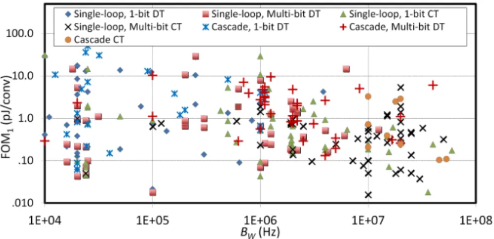
As mentioned in the previous section, an ADC with a 10-MHz signal bandwidth (referred as WBW) with a resolution of more than 12-bit, which translates into more than 75-dB SNDR, is considered for the second part of this proposal. It is a well-established fact that ∆ΣM is a unique option for targeted resolution and an acceptable figure of merit (FOM), as can be concluded from Figure 1.3. Essentially two scenarios are available to realize a ∆ΣM. 1) DT or switched capacitor (SC) implementation. 2) continuous time (CT) implementation. Having a glance at Figure 1.4, CT-∆ΣM is well-suited for high bandwidth applications because of the following justifications. 1) SC-∆ΣMs need amplifiers with high unity gain bandwidths (usually at least five times of the sampling frequency) to satisfy the settling accuracy requi-rements while no settling behavior is involved in CT-∆ΣMs which make them operate at higher sampling rate and/or with less power consumption. 2) Inherent anti-aliasing filtering is another unique feature of a CT-∆ΣM since the input signal is sampled at the output of CT loop filter hence significant suppression at the aliasing frequencies can be achieved. 3) For the SC-∆ΣM, design of the sampling network at the input of the modulator is a challenging task since sampling accuracy greater than the full resolution of the entire modulator is needed [8]. However, in the case of CT-∆ΣM sampler is inside the loop filter and any error caused by
Figure 1.3 Figure of Merit (FOM) against SNDR for various ADC architectures[6, 7] ( c [2016] IEEE, c [2016] IEEE)
sampling process accompany with quantization noise is easily suppressed by the gain of the loop filter in the desired bandwidth. However, CT-∆ΣMs suffer from clock jitter rather than SC-∆ΣMs. Although any timing error, injected to the sampler, is suppressed by the gain of loop filter, timing error of the feedback DAC is directly injected to the modulator input without any noise shaping and this effect significantly degrades the SNR of the modulator. Therefore, this effect must be minimized for high performance ∆ΣMs. Another drawback of the CT-∆ΣMs is the excess loop delay (ELD). Performance degradation and even instability may occur if the excess loop delay is too large. Fortunately, this effect can be alleviated by proper employing of ELD compensation techniques [9].
Regarding above explanations, A ∆ΣM, implemented in the CT regime, is opted for this research. But there is still some bottlenecks need to be carefully addressed. These bottlenecks are itemized as follows :
1. It is emphasized that CT-∆ΣM would be a good option for the wide bandwidth applications where active-RC, gm-C, and MOSFET-C integrators are usually utilized to implement the loop filter of the modulator [4]. In the voltage/current domain, operational amplifiers (op-amps) or operational transconductance amplifiers (OTAs) consume most of the power budget. Moreover, either lack of enough voltage headroom in the advanced node technologies (65 nm CMOS process and beyond) or shrinking the nominal voltage rate exacerbates the issues. A solution to this problem is to shift part of the design from voltage/current mode signal processing to the time mode signal processing [11]. There are two main benefits behind the time domain approaches. First there is no longer any concern related to the swing problems since the voltage/current
5
Figure 1.4 FOM1 (F OM1 = 2EN OB(bit)P (W ).output rate(S/s)) against BW for various types of ∆ΣMs
[10]( c [2018] John Wiley and Sons)
swing is translated into the time difference. Second, we can take the advantages of the digitally implementation of the analog blocks [12].
2. VCO-based quantizer (VCOQ), which is considered as one of the time mode ap-proaches, is an appealing option to implement part of a CT-∆ΣM with it. However, this architecture suffers from severe non-linearity caused by voltage to frequency cha-racteristics of the VCO. Multiple approaches have been addressed to linearize it and enhance the dynamic range [13]. These approaches can be categorized into embedding the VCOQ in a ∆ΣM loop or digitally calibrating the VCOQ non-linearity. In the first approach, a high-order ∆ΣM with power hungry op-amp is needed while digital cali-bration makes the system power consuming due to high speed look-up tables (LUTs) high sampling rate.
3. As mentioned earlier, higher order modulator, which is severely susceptible to instabi-lity, is needed for embedded VCOQs. To overcome this issue, multi stage noise shaping (MASH) ∆ΣM is an alternative. However, quantization noise must be extracted in a voltage/current domain and it adds circuit complexities. It will be shown that the quantization error can be extracted in a time domain with a simple digital circuit.
1.3 Research objectives
1.3.1 LBW ADC research objectives
To tackle the aforementioned problems in Section 1.2.1, an alternative is targeted in which the power hungry adder is eliminated. It is also planned to propose a power optimized fully
differential OTA. Therefore, it is worth investigating the new generation of the OTAs i.e. inverter-based OTA. To diminish the power consumption proper techniques must be adap-ted. Reducing the supply voltage is one of the solutions to do so. Reducing the supply voltage, however, has its own drawbacks e.g. lower voltage headroom. Therefore, an appropriate tech-nique must be chosen to alleviate those issues. Biasing the OTAs in the weak inversion is an appealing solution to lower the power consumption as well. However, circuits biased in the weak inversion are sensitive to the PVT variations. Self-biasing techniques could fix such an issue. Having had above discussion, the main objectives of this research are itemized as follows :
1. Our goal is to address a new DT-MASH ∆ΣM which satisfies the main requirements of a LBW ADC in terms of resolution and power consumption.
2. High-level synthesis must be performed to avoid over-designing and thus to optimize the design parameters.
3. New FF structure is proposed and quantization noise extraction is only performed by the available analog signals at the output of the integrator used in the proposed modulator.
4. In terms of circuit level technics, enough effort must be made on OTA selection since the OTAs are the most momentous part of a DT-∆ΣM.
1.3.2 WBW ADC research objectives
The strategy to tackle the aforementioned limitations in Section 1.2.2 is to propose a CT gated ring oscillator (GRO)-based MASH (CG-MASH ) structure. MASH structures are sensitive to the mismatch between analog coefficients and digital cancellation logic. Therefore, a high-gain operational amplifier is required to alleviate this effect. Quantization error extraction is another challenge in a CT MASH ∆ΣM. Therefore, proper quantization error extraction technique is required. That being said, the main objectives are listed as follows.
1. We plan to introduce a new CG-MASH ∆ΣM which is well-suited for high band-width applications. This also demonstrates a significant improvement compared to DT-MASH, single loop ∆ΣM with the same noise shaping capability and CT-MASH ∆ΣM.
2. Locate the main challenges and their solutions of the proposed CG-MASH in high level syntheses. Architectural level solutions are explored to overcome these challenges. 3. Use analog filter to delay and remove the quantization error of the first stage is
ad-dressed by using simple digital delay due to time nature of the quantization error in the proposed architecture.
7
1.4 General organization of the thesis
The main challenges of SC-∆ΣMs as well as VCO-based ∆ΣMs are reviewed in Chapter 2. As explained, SC-∆ΣMs with distributed feed forward paths suffer from a power-hungry adder located before the quantizer. Although, a passive adder can be used to save power, it is at the expense of pushing stringent requirements on the second OTA in the second order ∆ΣM. A comprehensive literature review is also performed in Chapter 2. The main drawbacks of the VCO-based quantizer is scrutinized and the main techniques to overcome the drawbacks are also reviewed.
This thesis is based on three journal papers to address mentioned drawbacks in Chapter 2. The first journal, which is presented in Chapter 3, mainly explores a new architecture to eliminate the power hungry-adder in a conventional feed forward topology. To do so, an less SC-∆ΣM is proposed and MASH structure ∆ΣM is formed based on the adder-less topology. A self-biased inverter-based OTA is then introduced where it is biased in the weak-inversion region. It is demonstrated that the OTA fails over slow process corners and low-supply voltage. To cope with that issue, a self and body biased inverter-based OTA is proposed.
Chapter 4 represents the second journal paper. During the research process, it is found that MASH ∆ΣMs are susceptible to the mismatch between analog loop filter and the digital cancellation logic. To overcome such a drawback, a modified SMASH ∆ΣM is proposed. The proposed SMASH ∆ΣM offers a better linearity compared to the conventional SMASH architecture. It also needs relaxed OTA DC-gain requirements.
Chapter 5 represents the third journal paper. It scrutinizes a new trend in the hybrid ∆ΣMs. The high-level synthesis of the proposed continuous time gated ring oscillator based MASH ∆ΣM is first presented. Main circuit imperfections are described as well. Chapter 5 then continues with the circuit level implementation of the proposed modulator as well as measu-rement results.
Chapter 6 provides a general discussion on the proposed ∆ΣMs. It describes the main features of the proposed ∆ΣMs. Final conclusion, main contributions of this research as well as suggestions for future work are all drawn in Chapter 7.
CHAPTER 2 LITERATURE REVIEW
As mentioned in the previous chapter, analog to digital converter (ADC) is one of the most crucial blocks in many electronic devices. ADCs are essentially categorized into the Nyquist rate ADCs as well as over-sampled and noise-shaping ADCs. Nyquist rate ADCs are not suitable options for high-resolution applications and even they are over-sampled, in many applications, to provide a medium resolution and relax the filtering requirements. Over-sampled and noise-shaping ADCs, known as ∆Σ ADCs, however provide special features over the Nyquist rate ADCs. Such ADCs can provide medium to high resolution with low precision building blocks. They also compromise between resolution and bandwidth. They can also be optimized at both system level and circuit level. This chapter, which focuses on the ∆Σ ADCs, is split into two main sections. In the first section, our literature review is mainly focused on the low bandwidth (less than 20 kHz) DT(SC)-∆ΣMs which is truly the foundation of the first proposed LBW ∆ΣM presented in the next chapter. The second part of this chapter is dedicated to WBW ∆ΣMs. Therefore, hybrid voltage and time modes ∆ΣMs are comprehensively reviewed.
2.1 Literature on LBW SC-∆ΣMs
Many state of the art high resolution low bandwidth (less than 25 kHz) modulators have been introduced. Single stage ∆ΣMs have been presented in [14–17] and [5] while MASH ∆ΣM for low bandwidth applications have been presented in [18, 19]. A fourth order single stage ∆ΣM has been introduced in [20] which took the advantage of the low-threshold voltage devices of a 0.13 µm CMOS process to operate at 1 V supply voltage. It is worth noting that single stage higher order (third order and more) modulators are severely susceptible to instability and the maximum out-of-band gain (Hinf ) of the N T F needs to be selected meticulously. Moreover, the modulator in [20] implemented as a fourth order FF structure and as will be described in the rest of this proposal, the power hungry adder is the main bottleneck of the FF structure which was resolved by employing the passive adder. This technique suffers from reducing the signal swing at the input of comparator and capacitors mismatch as well. Similar strategy has been adopted in [16] in which a 1.5 bit, fourth order FF structure was proposed for 20 kHz signal bandwidth. To resolve the problem of summation block, a switch matrix feedback compensation based on a direct summation technique [15] was adapted. Such a technique is well-suited for multi bit quantizer and not applicable for mono bit quan-tizer ∆ΣMs. Employing the multi bit quanquan-tizer itself has its drawbacks. Dynamic Element
9
Matching (DEM) technique needs to be utilized to mitigate the non-linearity problem of the DAC in the feedback path which obviously leads to the circuit complexity as well as power consumption.
2.2 Literature on WBW ∆ΣMs
2.2.1 ∆ΣMs with time-domain blocks
There are three common ways to represent a signal in electronic circuits ; Continuous Time Continuous Amplitude (CTCA), Discrete Time Discrete Amplitude (DTDA) and Discrete Time Continuous Amplitude (DTCA). Using time resolution of digital waveform to represent signals introduces the fourth way of signal representation i.e. Continuous Time Discrete Am-plitude (CTDA). There are two main benefits behind using this approach in today’s electro-nics. First, the power dissipation follows the rule of CV2f , which is the power dissipation of
a digital gate driving a load capacitance (C) and switching between 0 to V at the sample rate of (f ). The second benefit is that the supply voltage is virtually uncoupled from SN R since the signal swing is no longer represented in the voltage mode and it is in the time domain, instead. This feature is very important either for advanced node technology with low sup-ply voltage (Vdd < 1V ) or for the circuits operating at the fraction of nominal voltage rate.
This also makes the circuit dissipate less power in analogy with conventional voltage mode circuits. However, time domain circuits suffer from timing jitter since the representation in the time domain. To have a better insight, a comparison is performed for a unity gain buffer corresponding to the Figure 2.1 [21].
Assuming that the digital waveform has the slop of Vdd/tr for the rising and falling edge,
standard deviation of the voltage error is expressed by vσ and tσstands for standard deviation
of the timing error, tσ can be expressed as follow :
tσ = vσ dv/dt = vσtr Vdd (2.1)
For a CTDA signal with two transitions in every clock period (Ts) the upper limit of SN R
in the time domain is given by :
SN RT =
Ts2 16t2
σ
(2.2) Also the upper limit SNR for the voltage mode can be expressed as :
SN RV = V2 dd 8v2 σ (2.3)
Therefore, SN RT SN Rv = T 2 s 2t2 r (2.4) For the sampling frequency of 640 MHz and rise time of 28 pS, CTDA provides 63 dB SN R better than CTCA. Time to digital converters were originally proposed to measure single-shot pulses in nuclear experiments (A CMOS time to digital converter VLSI for high-energy physics). The schematic of TDC is depicted in Figure 2.2, in which the input propagates through a chain of digital buffers whose outputs are then fed into an array of D flip-flops while the stop signal latches the states of these flip-flops. Therefore, the output of flip-flops provides a thermometric representation which is time duration between input start signal and stop pulse.
Similar to ADCs, TDCs can also be categorized into Nyquist rate TDCs as well as oversam-pled noise shaping TDCs. Successive approximation (SAR) TDC has been addressed in [22] and pipeline TDC was proposed in [23]. Various configurations, which have been defined for ADC, can be defined for TDCs, as well. For example a two-step TDC has been proposed in [24]. In this topology the residual of the first stage is extracted and then is fed to the second stage for further process. The outputs of two-steps are digitally combined to form the overall output. Oversampled noise shaping TDCs have been widely used in time-of-flight (TOF) applications, positron emission tomography (PET), and all-digital phase-locked loops (ADPLLs) and etc. This type of data converter is also known as VCO-based quantizer in which the VCO acts as voltage to time converter and time information is then quantized by a bunch of counters. This class of data converter also has several members such as gated ring oscillator (GRO) [25], switched ring oscillator (SRO) [26], gated switched ring oscillator (GSRO) [27], VCO gated ring oscillator (VC-GRO) [28] and each of them has its own fea-tures, pros and cons. To conduct this research in a right path, three main categories have been investigated. 1) Nyquist rate TDCs used inside the loop filter of a delta sigma modulator. 2) VCO-based quantizer and its families as a standalone ADC/TDC, this category is referred to ring oscillator based data converter in section 2.2.1. 3) VCO-based quantizer used inside the loop filter of a delta sigma modulator.
Delta sigma modulators with embedded Nyquist rate TDCs
The use of amplitude-based quantizer such as FLASH, SAR or any other Nyquist rate ADC in a delta sigma loop filter is a design challenge thanks to voltage headroom limitations in advanced node technologies. Time/frequency coding instead of amplitude coding is an alternative to implement the quantizer inside the delta sigma loop filter. The most
momen-11
Figure 2.1 Translation of voltage noise to timing noise[21] ( c [2011] IEEE)
Figure 2.2 Basic single-shot TDC [21] ( c [2011] IEEE)
Figure 2.3 (a) Conventional multi-bit delta sigma modulator.(b) Time-domain quanti-zer/DAC based delta sigma modulator [21] ( c [2011] IEEE)
tous advantage of this realization is that this technique is well-suited for sub-micron CMOS processes with low supply voltage. However, timing errors must be carefully scrutinized in
Figure 2.4 Simplified schematics of the TDC used as quantizer in a CT-DSM [21] ( c [2011] IEEE)
this scenario. A CT-∆ΣM based on a time encoding quantizer (TEQ) has been addressed in [29]. This modulator shows the performance of the multi-bit CT-∆ΣM while the com-plexity is similar to single bit CT-∆ΣM by replacing the FLASH quantizer, DAC and its mismatch correction circuitries with TEQ similar to PWM modulator to reduce the silicon area at the expense of faster clock in the TEQ. A multi-bit CT-∆ΣM using time domain quantizer and feedback element has been proposed in [21]. Figure 2.3 shows the conventio-nal multi-bit CT-∆ΣM along with the modulator proposed in [21]. In this architecture, the PWM-generator followed by TDC replaces the multi-bit quantizer and multi-bit DAC. The PWM block converts the voltage information to a pulse stream whose width is proportional to the amplitude of its input signal for every clock period. Digital codes at the output of the TDC correspond to the time edges of its input and it generates time-quantized feedback pulse, as well. Noise shaping is performed by a third order quasi-inverse-Chebyshev filter while both quantization noise of the TDC and non-linearity error of the PWM generator are noise-shaped. 1-bit DAC is used to provide feedback current pulse the time quantized digital waveform. The TDC used as a quantizer has been designed to generate 50 quantization steps in 4 nS period and the simplified schematic of the TDC is depicted in Figure 2.4 in which 50 clock phases are generated by a chain of inverters. Each phase is then used to drive the clock input of a flip-flop. The first 25 flip-flops are driven by PWM output pulse and the rest of 25 flip-flops are driven by complement of the PWM output pulse and OR-gate is in charge of accommodation of 25 inputs. Designed in 65 nm CMOS process, this architecture showed the SN DR of 60 dB over 20 MHz signal bandwidth while output rate is 250 MSPS.
Standalone ring oscillator based data converters
As mentioned in the previous chapter, design of an ADC in deep sub-micrometer CMOS pro-cesses is a challenging task due to low supply voltage as well as technology scaling. However,
13
Figure 2.5 Barrel shifting occurs through delay elements across different measurements [30, 31] ( c [2008] IEEE, c [2009] IEEE)
for time domain circuits, time resolution is enhanced from the reduced transition of digital signals, which is in sort of tens of picoseconds in 90 nm CMOS and below. In a VCO-based ADC, input voltage is translated to a time-based signal whose frequency is proportional to the analog input. The frequency is then quantized by counting the edge of the VCO’s output during the sampling period [30, 31]. Since the VCO produces a continuous phase output, the quantization noise of the previous sample affects that of current sample and hence and inherent first order noise shaping property can be obtained. Another important feature of a VCO-based ADC is that this topology consists of a ring oscillator followed by digital cir-cuits. Therefore, sample rate of this architecture could be up to gigasamples per second in advanced node CMOS processes. VCO-based ADC also offers an appealing feature which is inherent dynamic element matching. As depicted in Figure 2.5, the VCO-based quantizer dynamically shuffles through delay stages in a barrel shift fashion as the measurement of edges in each reference period progress. Therefore, if the frequency is output variable of the quantizer, mismatch in delay across the stages is effectively first order noise shaped [30][31]. This feature is very important especially in the case of embedding a VCO-based quantizer inside the loop filter of a ∆ΣM. The reason is that such a barrel shifting pattern and the resulting noise shaping is identical to the output pattern of the data weighted averaging (DWA) DEM algorithm. Therefore there is no need to implement an explicit DEM at the feedback path of the ∆ΣM.
Due to mentioned unique features of the VCO-based quantizer, there has been a mass of re-search on it. Some publications have addressed a comprehensive analyses on VCO, techniques
Figure 2.6 Two-step VCO-based delta sigma ADC architecture [32] ( c [2015] IEEE)
to mitigate its voltage-to-frequency non-linearity [32, 33], other papers have introduces some applications [33–35], and the other have embedded the VCO-based quantizer inside the loop filter of a ∆ΣM [30, 31, 13]. Although the latter is a technique to mitigate the non-linearity issue of a VCO-based quantizer, we are going to be investigating them in a separate section due to its importance. A comprehensive analysis of a VCO-based quantizer was published in [33] in which jitter, nonlinearity, mismatch, and the metastability of D flip-flops have been investigated. A two-step VCO-based delta sigma ADC has been introduced in [32, 36] in which a coarse VCO-based ADC digitizes the analog input signal while generation the nonlinearity. Then the quantization error is extracted and then the second VCO-based ADC digitizes the residue. Two outputs are summed up to generate the overall output. Two tech-niques are used in this structure. First, the severe non-linearity of the coarse VCO-based ADC is noise shaped by the fine VCO-based ADC. Second, the fine VCO-based ADC does not suffer from non-linearity since it is fed by a low swing analog signal. This architecture is shown in Figure 2.6. Fabricated in 40 nm CMOS process, the proposed two-step VCO-based ADC [32] shows the SN DR of 59.5 dB over the bandwidth of 40 MHz with the sampling frequency of 1.6 GHz. A 0-2 MASH VCO-based ∆ΣM has been recently reported in [37], based on traditional MASH 0-2 structures [38, 39], as illustrated in Figure 2.7. Unlike the traditional 0-2 MASH structure, which uses Nyquist rate ADCs to implement the first stage, a VCO-based ADC which offers a first order noise shaping was used to implement the first stage [37]. Therefore noise leakage due to imperfect matching will be first-order shaped. But the first stage does not provide any further noise shaping and that is why this architecture
15
Figure 2.7 (a) Block diagram of a VCO-based 0-delta sigma MASH ADC, (b) Signal model of the proposed MASH ADC [37] ( c [2015] IEEE)
was called MASH 0-2. The same method as presented in [32] was used to tackle non-linearity problem and the second stage just process the noise shaped quantization noise hence input voltage swing is greatly reduced. Regarding the signal model, shown in Figure 2.7(b), where E1,2 are quantization noise of the first and second stage respectively. KQ1,2 are the gain of the
quantizers. KDAC/G3 represents the gain of DACs and finally H(s) is the ∆ΣM loop filter.
Under perfect matching, E1 and DQ1 are fully cancelled and quantization noise of the second
stage is noise shaped by H(s). It should be mentioned that similar idea was proposed in [40] but no silicon was reported.
By taking the advantage of PWM signal, a highly linear VCO-Based ADC has been proposed in [41]. In this architecture, the analog voltage is first converted into a 2-level PWM signal using a naturally sampled PWM generator. The output of the PWM generator drives the VCO hence VCO operates at two frequencies i.e. fhigh and flow resulting linear operation of
are selected. We can conclude that the linearity problem moved back to the PWM generator. Fortunately, PWM generator can be made more linear than VCO. Moreover, the harmonics of carrier frequency of the PWM are located outside the signal bandwidth and can be removed by digital decimation filter. This architecture is illustrated in Figure 2.8. Using similar technique, a MASH 1-1 VCO-based ADC was proposed in [42], as shown in Figure 2.9. Unlike the architecture proposed in [41], a high-performance asynchronous delta sigma modulator (A∆ΣM ) was utilized to generate PWM signal. The PWM signal is then controls the VCO. Quantization noise of the first stage is extracted using an array of phase detectors and the resulting error is applied to the second stage. Since the first VCO operates at two operation points it has linear performance. For the second VCO, the input signal is a low-swing analog signal and it shows linear performance as well. By proper selecting the carrier frequency of the A∆ΣM, harmonic distortion can be located outside the desired bandwidth.
Ring oscillator based ADC has other members such GRO, SRO, GSRO and VC-GRO. Getting started with the GRO paves the way to understand the rest of the structures. The concept of GRO was first proposed in 1997 and then it was extended and analyzed in 2009 [25]. The structure of GRO is illustrated in Figure 2.10, which shows the key concept of GRO. It’s ope-ration as simple as oscillation when the power supply is on and freezing its phases whenever the power supply is switched off. Similar to the VCO-based quantizer, the residue occurring at the end of a given measurement pulse can be transferred to the next measurement inter-val. This makes this architecture operate as a first order noise shaping quantizer like its first generation i.e. VCO-based quantizer. Numerous papers have been published just reporting either standalone GRO-based quantizers or its application in the PLLs or ADPLLs [43–46]. GRO-based MASH 1-1 topology has also been addressed in [47–49]. Based on the concept of the GRO , time-domain error feedback filter and MASH structure, a fourth order delta sigma time to digital converter has been addressed in [50]. The configuration is shown in Figure 2.11. The first stage is a standalone GRO-based TDC that presents first order noise shaping. Quantization error of the first stage, which is the time domain, is then extracted to feed to the second stage. Second stage of this architecture is a third order delta sigma TDC. This stage consists of a GRO-TDC as a core while the quantization error, which is aslo represented in the time domain, is extracted. Instead of using conventional integrator, a time domain error feedback, as shown in Figure 2.11, is used to provide extra 2nd order noise
shaping. The architecture proposed in [50] offers a fully time domain delta sigma TDC. Regarding the ring-oscillator based ADCs, have been reviewed up to now, there are noticeable issues which are itemized here. 1) Performance of the VCO-based ADC is limited by the non-linear voltage-to-frequency transfer characteristic of the VCO but its unique features such as first order noise shaping and inherent dynamic element matching is alluring and irreplaceable.
17
Figure 2.8 PWM-generator followed by VCO-based ADC [41] ( c [2011] IEEE)
Figure 2.9 PWM-generator followed by VCO-based ADC [42] ( c [2012] IEEE)
2) Two-step VCO-based ADC could resolve this problem to some extend but the VCO-based ADC located in the first stage is still experiencing full input swing, resulting nonlinearity. 3) In the case of VCO-based ADC controlled by PWM signal or even in the case of GRO-TDC, although the VCO or GRO behaves linearly, in fact the non-linearity property moved back to the PWM block. However, PWM generator can be designed with superior linearity. 4) Open loop MASH 1-1 structures are quite sensitive to the delay of quantization error generator.
Delta sigma modulators with embedded VCO-based quantizer
As mentioned in the previous section, the performance of the VCO-based quantizer is seve-rely limited by nonlinearity of the VCO’s voltage-to-frequency transfer characteristic since increasing the signal power makes the VCO exercise the entire non-linear range. Therefore, severe distortion appears at the output of the VCO-based ADC. To simultaneously suppress the VCO nonlinearity and increase the order of noise shaping the VCO-based ADC was em-bedded inside the ∆ΣM’s feedback loop as a first order noise shaping quantizer, as illustrated in Figure 2.12 [30, 31].
Figure 2.10 Gated ring oscillator TDC [25] ( c [2009] IEEE)
Figure 2.11 GRO-based MASH 1-3 and its timing error feedback filter [50] ( c [2015] IEEE)
In this topology, loop filter (L(s)) suppresses the VCO nonlinearity to extend its SN DR. It is apparent that the higher order loop filter, the better non-linearity suppression and as a consequence the better performance in terms of SN DR. This also means that the effectiveness of this technique greatly depends on the gain of the loop filter. The VCO-based ADC’s input spans the entire signal range and therefore it exercises the entire nonlinear tuning curve of the VCO. That is why high gain loop filter is needed to suppress the large amount of distortion caused by the VCO. For example, for a fixed OSR of 32, a standalone 31-level VCO-based quantizer presents 62 dB SN DR while the SF DR is about 35 dB. Increasing the order of
19
Figure 2.12 CT-∆ΣM with VCO-based quantizer [13, 30, 31] ( c [2012] IEEE, c [2008] IEEE, c
[2009] IEEE)
the loop filter results the SN DR and SF DR of 86 and 58 dB, respectively. Further analysis shows that at least third order loop filter is required to achieve an SF DR of 88 dB. It is worth mentioning that third order loop filter along with first order quantizer results a forth order ∆ΣM. Not only does such a higher order ∆ΣM suffer from higher level of complexity and power consumption but it is also prone to instability. In the modulator proposed in [30], VCO output frequency was used for design variable since it has proportional relationship with the input signal. As a result, to exercise the full dynamic range of the VCO-based quantizer, the VCO input signal must span the entire the non-linear transfer characteristics. To avoid spanning this non-linear transfer characteristic, output phase of the VCO was used in [31] to form a fourth order CT-∆ΣM. Before reviewing the architecture proposed in [31], it is worth spending more time on the voltage-to-phase VCO ADC. Figure 2.13 shows the block diagram of a voltage-to-phase VCO ADC. Here, the VCO phase is sampled and quantized by registers and a phase detector compares the registers output with the reference phase by employing a simple phase detector. The resulting signal is fed into the input of a DAC and resulting analog signal is subtracted from the input signal. The residue is then applied to the VCO and the VCO provides integration for the next cycle. Since the VCO serves as an integrator and a negative feedback is formed this architecture is actually a first order CT-∆ΣM. Both voltage-to-frequency VCO ADC and voltage-to-phase VCO ADC is modeled and simulated in CPPSIM simulator for 1GHz sampling frequency over 20 kHz signal bandwidth while the same non-linearity is considered for both case. It can be concluded from Figure 2.14 that in the case of voltage-to-frequency VCO ADD SN DR is primarily limited by the distortion
Figure 2.13 Voltage-to-phase VCO-based ADC [31] ( c [2009] IEEE)
while in the case of voltage-to-phase VCO ADC the distortion tones are almost eliminated and provides 36 dB SN DR improvement rather than the latter case. The voltage-to-phase VCO ADC [31] was employed inside a forth order ∆ΣM to provide the SQN R of about 95 dB over 20 MHz signal bandwidth, as shown in Figure 2.15. Cascade of integrators with feed forward distribution was used to lower the integrator output swings.
To avoid using higher order single loop modulator as well as getting rid of the nonlinearity problem of a VCO, a residue-cancelling VCO-based quantizer has been addressed in [13, 51] and it was employed in a first order CT-∆ΣM to form a second order CT-∆ΣM, as depicted in Figure 2.16. The idea behind the residue-cancelling VCO-based quantizer is to minimize the voltage swing at the input of the VCO. To do so, a FLASH ADC digitizes the input voltage signal while the output digital codes are converted back to the analog signal using a DAC and the resulting signal is subtracted from analog input signal. The residue, which is sitting down inside the linearity range of the VCO, is then control the VCO. The VCO based ADC digitizes this quantization error and finally the output of FLASH ADC and VCO-based ADC are combined to generate the output bit stream. It is worth noting that a similar architecture was proposed before in [52].
Another technique to circumvent the non-linearity problem of the VCO-based quantizer has been introduced in [53] in which the nonlinearity problem was resolved outside the loop filter instead of embedding it inside the loop filter of ∆ΣM. The idea behind this modulator is that the first stage is a conventional first order SC-∆ΣM while the quantization noise of the first stage is extracted and the injected to a VCO-based quantizer. The outputs of two stages are added using a DCL hence a MASH 1-1 is formed. Since the input of the VCO is just a quantization error, the VCO does not exercise the whole non-linear range and therefore it operates almost linearly. Another main feature of this architecture is that the VCO-based
21
Figure 2.14 PSD of (a) voltage-to-frequency VCO ADC [30], (b) voltage-to-phase VCO ADC [31] ( c [2008] IEEE, c [2009] IEEE)
Figure 2.15 Fourth order CT-∆ΣM with voltage-to-phase VCO-based ADC [31] ( c [2009] IEEE)
quantizer operates 12 times faster than the first stage. Therefore, not only does not the first stage suffer from stringent requirements on op-amp, but the SN DR goes up similar to what occurs in a multi-rate ∆ΣMs.
Having reviewed above four techniques to mitigate the non-linearity of the voltage-to-frequency transfer characteristic, there are several issues. First, embedding the voltage-to-frequency VCO-based quantizer inside the loop filter needs high-order modulator which is susceptible to instability and the power consumption of such architectures is not negligible. In the case of voltage-to-phase VCO ADC, although the nonlinearity problem is relatively improved, it
Figure 2.16 Second order CT-∆ΣM with residue-cancelling VCO-based quantizer [13] ( c [2012] IEEE)
still needs a higher order modulator. Another problem is that this VCO-based ADC no longer offers an inherent dynamic element matching since there is not differentiator at the back-end of the VCO-based quantizer. In the case of residue cancelling VCO-based quantizer, FLASH ADC accompany with DAC and it error correction circuitry must be used to generate residue hence it costs silicon area as well as power consumption. And finally, in the case of multi-rate MASH structure followed by VCO-based quantizer there are two issues ; 1) This architecture is not potentially suitable for high band width application because of the technology limita-tion in SC-implementalimita-tion. 2) Multi-bit quantizer must be used inside the loop of the first stage to reduce the quantization error and confine it in the linear range of the VCO-based quantizer.
2.3 Conclusion
Literature review has been performed on SC-∆ΣM to design a LBW SC-∆ΣM to cover 20 kHz signal bandwidth. It has been inferred that both system level optimization as well as circuit level techniques must be properly used to have a power optimized SC-∆ΣM. From the second part of the literature review, it has been concluded that CT-∆ΣM is the best option for high resolution high bandwidth application. To make the design suitable for advanced CMOS process with low supply voltage, part of the design can be implemented in the time domain. In doing so, Nyquist rate TDC as well as VCOQ have been used. Nyquist rate TDC does not offer any noise shaping while VCOQ offers this feature. It also has implicit DEM property. However, this class of ADC severely suffers from non-linearity.
23
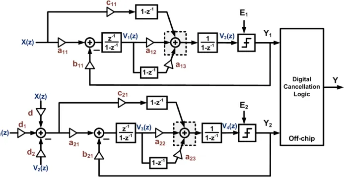
CHAPTER 3 ARTICLE 1 : A 0.9-V 100-µW FEEDFORWARD
ADDER-LESS INVERTER-BASED MASH ∆Σ MODULATOR WITH 91-dB DYNAMIC RANGE AND 20-kHz BANDWIDTH
3.1 Overview
As described in the previous sections, conventional FF topology suffers from a power hungry adder to sum up the feed forward branches. This issue is addressed in this chapter by moving back the adder to the input of the second integrator in the second order ∆ΣM. The quanti-zation error is extracted in the voltage domain and then fed into the back-end stage which is similar to the front-end stage. A self and body biased inverter-based OTA operating in the weak inversion is also proposed to overcome the issues related to the weak-inversion region. The following sections are the reproduction of an accepted article in IEEE Transactions on Circuits and Systems-I : Regular Papers
— Article 1 : M. Honarparvar, J. M. de la Rosa and M. Sawan, "A 0.9-V 100-µW Feed-forward Adder-Less Inverter-Based MASH∆ΣModulator With 91-dB Dynamic Range and 20-kHz Bandwidth," in IEEE Transactions on Circuits and Systems I : Regular Papers, vol. 65, no. 11, pp. 3675-3687, Nov. 2018 [54].
3.2 Abstract
A 0.9-V ∆Σ modulator integrated in a 0.18-µm CMOS technology for digitizing signals in low-power devices is presented in this paper. To do so, a cascade (MASH) architecture based on an adder-less feedforward structure is proposed. The proposed modulator has a unity signal transfer function in both stages of the modulator in order to reduce the integrators output swings. To mitigate the failure of slow process corner in the weak inversion as well as to further diminish the power consumption of the presented modulator, a fully differential self and bulk biased (SBB) inverter-based OTA is proposed. Experimental results are shown to demonstrate the efficiency of the proposed ∆Σ converter, showing state-of-the-art perfor-mance, by featuring 88.7-dB SNR, 86.4-dB SNDR and 91-dB DR within a signal bandwidth of 20-kHz, with a power dissipation of 103.4-µW when the circuit is clocked at 5.12-MHz. Key Words : Analog-to-digital conversion, delta-sigma modulation, switched-capacitor cir-cuits, inverter-based OTAs.
3.3 Introduction
The need for hand-held devices, smart-phones and medical implantable microelectronic sys-tems, is remarkably growing up. However, keeping all these electronic devices power optimized is one of the main challenges due to the lack of life-time batteries utilized to power them up. One of the most critical building blocks of such devices is the analog-to-digital converter (ADC), since it needs to efficiently digitize acquired signals in a hostile environment. Com-pared to other ADC techniques, Delta-Sigma Modulators (∆ΣMs) have been widely used in those devices due to the unique features they offer and they are capable of being effec-tively power optimized at both architectural and circuit levels [2]-[55]. Nevertheless, special care must be taken into account to optimize the performance of ∆ΣMs. Indeed, many state-of-the-art high-resolution (>14-bit) low-bandwidth (<25-kHz) ∆ΣMs have been reported, including single-stage architectures [56]-[5] and cascade topologies – also referred to as Multi stAge noiSe sHaping (MASH) [2]-[19]. Among other ∆Σ loop-filter topologies, the so-called feedforward (FF) structure has been successfully used by some designers to implement single-stage high-order (third-order or more) noise shaping [20]-[16]. However, the main limitation of FF structures is the power-hungry adder required at the input of the quantizer. This adder constitutes one of the main design bottlenecks of FF ∆ΣMs employed in ADCs, where the energy consumption becomes critical. In order to mitigate this limitation, some authors have proposed alternative implementations of the FF loop-filter. Thus, the ∆ΣM reported in [20] includes a fourth-order FF loop-filter with a passive adder. However, this technique suffers from both reduction of signal swing at the input of the comparator, and mismatch between capacitors. A similar strategy has been adopted in [16], where a 1.5-bit (3-level), fourth-order FF structure is proposed for digitizing signals with a 20-kHz bandwidth. Another approach consists of using switch matrix feedback compensation based on a direct summation tech-nique as proposed in [15]. While such techtech-nique is well-suited for multi-bit quantizers, it is not applicable to single-bit ∆ΣMs. Moreover, employing multi-bit quantizers in high-resolution applications is limited by the inherited nonlinearity of the DAC used in the feedback path of the ∆Σ modulator. This requires using linearization techniques, such as dynamic element matching (DEM), which obviously leads to increasing the circuit complexity as well as the power consumption. Similar FF topologies have been addressed in [57]-[58] where the last integrator serves as an integrator and an adder simultaneously. However, an extra DAC in the feedback path is needed to retrieve the noise transfer function (NTF) of the modulator. It is worth noting that in all above-mentioned topologies, an extra DAC is required to extract the quantization noise if they are supposed to be used in a MASH configuration and hence adds circuit complexity.
![Figure 2.4 Simplified schematics of the TDC used as quantizer in a CT-DSM [21] ( c
[2011] IEEE)](https://thumb-eu.123doks.com/thumbv2/123doknet/2333102.32139/30.918.221.697.106.330/figure-simplified-schematics-tdc-used-quantizer-dsm-ieee.webp)
![Figure 2.5 Barrel shifting occurs through delay elements across different measurements [30, 31] ( c
[2008] IEEE, c
[2009] IEEE)](https://thumb-eu.123doks.com/thumbv2/123doknet/2333102.32139/31.918.214.695.110.394/figure-barrel-shifting-occurs-delay-elements-different-measurements.webp)
![Figure 2.11 GRO-based MASH 1-3 and its timing error feedback filter [50] ( c
[2015] IEEE)](https://thumb-eu.123doks.com/thumbv2/123doknet/2333102.32139/36.918.120.851.472.747/figure-based-mash-timing-error-feedback-filter-ieee.webp)
![Figure 2.15 Fourth order CT-∆ΣM with voltage-to-phase VCO-based ADC [31] ( c
[2009] IEEE)](https://thumb-eu.123doks.com/thumbv2/123doknet/2333102.32139/39.918.197.719.480.744/figure-fourth-order-sm-voltage-phase-based-ieee.webp)
![Figure 2.16 Second order CT-∆ΣM with residue-cancelling VCO-based quantizer [13] ( c
[2012] IEEE)](https://thumb-eu.123doks.com/thumbv2/123doknet/2333102.32139/40.918.170.749.112.362/figure-second-order-residue-cancelling-based-quantizer-ieee.webp)