A CMOS 90NM DIGITAL PIXEL SENSOR INTENDED FOR A VISUAL CORTICAL STIMULATOR
ROULA GHANNOUM
D´EPARTEMENT DE G ´ENIE ´ELECTRIQUE ´
ECOLE POLYTECHNIQUE DE MONTR ´EAL
M ´EMOIRE PR´ESENT ´E EN VUE DE L’OBTENTION DU DIPL ˆOME DE MAˆITRISE `ES SCIENCES APPLIQU ´EES
(G ´ENIE ´ELECTRIQUE) AVRIL 2010
c
´
ECOLE POLYTECHNIQUE DE MONTR´EAL
Ce m´emoire intitul´e :
A CMOS 90NM DIGITAL PIXEL SENSOR INTENDED FOR A VISUAL CORTICAL STIMULATOR
pr´esent´e par : Mme. GHANNOUM Roula.
en vue de l’obtention du dipl´ome de : Maˆıtrise `es Sciences Appliqu´ees a ´et´e dˆument accept´e par le jury constitu´e de :
M. BRAULT Jean-Jules, Ph.D., pr´esident.
M. SAWAN Mohamad, Ph.D., membre et directeur de recherche. M. ZHU Guchuan, Doct., membre.
“Learn from the mistakes of others. You cannot live long enough to make them all yourself.” - Eleanor Roosevelt
Acknowledgments
My opening acknowledgments go to my research director, Professor Mohamad Sawan, who gave me the opportunity to get involved in such an interesting research topic. My thanks extend beyond my graduate studies since his welcoming me in his research group for an internship is what had opened this door of possibilities to me in Canada. I would like to emphasize his patience and support.
I would also like to thank Professor Jean-Jules Brault and Professor Guchuan Zhu for agreeing to be part of the Jury of this Master’s thesis, and taking the time to read this manuscript.
The graduate studies would not have been as interesting without my colleagues from the Polystim team. I would like to thank Delia-Alexandra Doljanu who was my internship supervisor at the beginning of my journey with Polystim, and who has always been a continuous source of inspiration and encouragement. I would also like to thank Louis-Francois Tanguay, our “expert” on the CMOS 90nm technology who good-humoredly answered a lot of my questions as I closed in to my chip submission deadline, and Olivier Valorge who gave me some input on capacitance design. And of course the whole team of people with whom I lived on daily basis, Jonathan Coulombe for making the Cortivision project so coherent, Pierre-Yves Robert for his jokes, Amer-Elias Ayoub for listening to “Muse” all day long, F´elix Ch´enier for his funny drawings on the whiteboard amongst the technical gibberish, Charles Robillard who made our lab inviting with beautiful pictures of Europe, Guillaume Desjardins whose presence made some of my courses less painful, S´ebastien Ethier for being such a good friend, Tarek Ould-Bachir for his witty sarcasm and not to forget my colleagues and friends from the other labs Rahul Singh, Max-Elie Salomon, Vincent Binet, Benoit Gosselin, Fay¸cal Mounaim and Saeid Hashemi - and of course Adeline Zbrezski and Laurent Faniel who had brief, yet unforgettable, stays in our labs. I would also like to extend my thanks to Ghyslaine Ethier-Carrier for making things easier, to Nathalie L´evesque for finding me odd jobs around school, to Marie-Yannick Laplante who is always there to cheer you up, and to R´ejean Lepage who has suffered with my PC and Cadence installation all throughout my studies.
my potential and without whom I would never have reached where I am today; and of course my brother Anthony who was always open to both personal and technical discussions; and my dearest friend Yolande for lifting up my spirits all the way from across the ocean.
My closing acknowledgements go to the Canadian Microelectronics Corporation for their technical support and to NSERC and Canada Research Chair on Smart Medical Devices for their financial support.
R´
esum´
e
La capture d’images et le traitement d’images et de signaux font partie des domaines les plus en vogue de nos jours. Un autre domaine qui retient l’attention des chercheurs `
a travers le monde est celui qui regroupe les applications biom´edicales - en particulier celles qui font le pont entre l’´electronique et la biologie. L’´equipe Polystim œuvre sur diff´erents projets `a la pointe de la technologie qui touchent `a ces domaines, dont le projet Cortivision: un stimulateur visuel cortical. Le syst`eme englobe la capture et le traitement d’images ainsi que la stimulation du cortex pour donner une certaine perception d’images aux patients souffrant de c´ecit´e. Le but de ce travail est de concevoir le module de capture d’images de ce syst`eme. Les modes d’op´eration du capteur d’images doivent ˆetre configurables par l’usager. Il doit se distinguer par une gamme dynamique ´elev´ee, une consommation de puissance r´eduite, une haute vitesse d’acquisition, une surface r´eduite, la portabilit´e, la possibilit´e d’avoir du traitement d’images sur puce, et la facilit´e de l’int´egrer dans un syst`eme sur puce avec le reste des modules de Cortivision. Un DPS (Digital Pixel Sensor) CMOS a ´et´e con¸cu et fabriqu´e avec la nouvelle technologie CMOS 90nm. Chaque pixel comprend une photodiode, un circuit de conversion de photocourant, un convertisseur analogique `a num´erique et une m´emoire num´erique de 8 bits, dans une surface de 9 µm x 9 µm avec un facteur de remplissage de 26% et 57 transistors. Le capteur offre plusieurs modes d’op´eration:
• Un mode d’int´egration lin´eaire.
• Un mode logarithmique avec une gamme dynamique ´etendue qui permet d’acc´eder aux pixels ind´ependamment du temps mais avec une diminution de lin´earit´e et un bruit plus prononc´e.
• Un mode diff´erentiel qui soustrait deux images successives `a mˆeme la puce pour obtenir une image binaire. Ce mode permet d’acc´el´erer le traitement d’images et fonctionne `a une vitesse plus ´elev´ee. Il peut ˆetre utilis´e simultan´ement avec le mode lin´eaire ou avec le mode logarithmique.
• Un mode d’expositions multiples qui est une option du mode lin´eaire pour augmenter la gamme dynamique, mais qui aurait l’effet de r´eduire la vitesse d’acquisition.
Des prototypes de puces ont ´et´e fabriqu´es avec la technologie CMOS 90nm offerte par STMicroelectronics avec des matrices de 64x48 pixels et un module de test avec plusieurs points d’acc`es pour caract´eriser la puce. Un PCB dot´e d’une architecture tr`es flexible a aussi ´et´e con¸cu et fabriqu´e afin de tester la puce et de l’interfacer avec un contrˆoleur VHDL implant´e dans un FPGA Spartan-3. L’impl´ementation finale d´emontre une r´eduction d’un facteur de trois de la surface du pixel compar´e `a une architecture moins r´ecente impl´ement´ee en CMOS 0.18µm dans le Laboratoire de Neurotechnologies Polystim, tout en proposant une m´ethode pour r´egler une fuite potentielle de l’obturateur du pixel en atteignant un d´ebit d’au moins 400 images par seconde. Par contre, les courants de fuite de la technologie CMOS 90nm ont contribu´e `
a un d´ecalage non-n´egligeable entre les mesures exp´erimentales et les simulations “post-layout”. Une partie des r´esultats a fait l’objet d’un article de conf´erence IEEE intitul´e “A 90nm CMOS Multimode Image Sensor Intended for a Visual Cortical Stimulator”.
Abstract
The image sensing and image processing fields make up some of the hottest topics in today’s industrial and research communities. Another field that is getting a lot of attention is biomedical applications - especially the combination of electronics to biology. The Polystim team is working on some state-of-the-art projects encompassing all that. One of these is the Cortivision project that consists of a visual cortical stimulator. The system comprises image sensing, image processing, and brain cortex stimulation to help blind patients acquire a sense of visual perception.
The goal of this work is to cover the image sensing portion of the system. This requires the design and implementation of an image sensor which is user configurable to operate in several modes, has a high dynamic range, low power consumption, high frame rate capability, reduced surface area, is portable, allows some on-chip image processing, and can easily be integrated in a system-on-chip with the rest of the Cortivision modules.
A CMOS Digital Pixel Sensor was designed and fabricated using the novel CMOS 90nm technology. Each pixel consists of a Photodiode, a photo-current conversion circuit, an Analog-to-Digital Converter and a digital 8-bit memory. It has a pixel pitch of 9µm with a Fill-Factor of 26% and 57 transistors. The sensor offers several modes of operation:
• A linear integration mode.
• A logarithmic mode that extends the dynamic range and allows time-independent pixel access at the cost of a forsaken linearity and an increase in noise.
• A differential (or better termed difference) mode that allows subtracting two consecutive frames to obtain a binary image. This mode helps speed up the im-age processing and allows a very high frame rate. It can be used in conjunction with either the linear or the logarithmic modes of operation.
• A multiple exposure mode that can be used in combination with the linear mode to increase the dynamic range at the expense of a decrease in frame rate. Prototype chips were manufactured using the CMOS 90nm process offered by
STMicroelectronics with 64x48 pixel matrices and a test module with different ac-cess nodes to characterize the design. A PCB was also designed and manufactured with a very flexible architecture to allow testing the chip and interfacing it with a VHDL controller implemented using a Spartan-3 Development Board. The final implementation shows a three-fold reduction in the surface area of the pixel as com-pared to a less recent architecture implemented in CMOS 0.18µm at the Polystim Neurotechnologies Lab, all while putting forth a method for circumventing shutter leakage while still reaching an acquisition rate exceeding 400 frames per second. Nev-ertheless, current leakage in the CMOS 90nm technology has led to a substantial discrepancy between experimental measurements and post-layout simulation results. An IEEE paper entitled “A 90nm CMOS Multimode Image Sensor Intended for a Visual Cortical Stimulator” sheds some light on part of the results.
Condens´
e
Le but de ce travail est de concevoir et d’impl´ementer un syst`eme de capture d’images capable d’acqu´erir des images de qualit´e `a un d´ebit ´elev´e tout en ´etant flexible, portable, et capable de transmettre des images `a un module de traitement qui est charg´e de reconstituer une image tridimensionnelle. Cette image serait ensuite ´
echantillonn´ee et utilis´ee pour stimuler le cortex visuel par des courants transmis par des micro´electrodes cr´eant des points de lumi`ere (des phosph`enes). Ceci est consid´er´e comme une extension des travaux de notre ´equipe en CMOS 0.18µm [1].
Pour parvenir `a cela, une revue des capteurs d’images ´electroniques ´etait n´ecessaire pour ´etablir une comparaison entre les capteurs CCD et les CMOS, pour conclure que les capteurs CMOS sont mieux adapt´es `a notre application, Cortivision, car ils perme-ttent d’int´egrer plusieurs fonctionnalit´es et modules `a mˆeme la puce - ce qui essentiel pour cr´eer des syst`emes compacts `a basse consommation de puissance. De plus, les capteurs CCD constituent une charge capacitive non-n´egligeable qui est plus difficile `
a int´egrer dans un syst`eme. Aussi, la qualit´e d’image des capteurs CMOS est dev-enue assez proche de celle des CCD ces derni`eres ann´ees, tout en offrant la possibilit´e d’avoir un d´ebit plus ´elev´e `a cause des convertisseurs analogique `a num´erique (CAN) int´egr´es sur la puce, et en ayant une sortie num´erique qui est plus pratique qu’une sortie analogique. Le proc´ed´e de fabrication CMOS est aussi moins dispendieux que le proc´ed´e CCD, et nous est disponible `a travers la CMC et STMicroelectronics. Ce proc´ed´e permet aussi un redimensionnement moins compliqu´ee de la matrice de pixels ainsi que la s´election d’une sous-fenˆetre de la matrice.
La conception du capteur a mis l’emphase sur l’acquisition d’images de bonne qualit´e `a un d´ebit ´elev´e pour ne pas ˆetre le goulot d’´etranglement du syst`eme de traitement d’images 3D. Ceci inclut la conception d’un CAN pr´ecis avec une assez haute fr´equence d’op´eration. La cam´era con¸cue offre `a l’usager la possibilit´e de choisir parmi plusieurs modes d’op´erations lin´eaires ou logarithmiques. Le mode lin´eaire est le pr´ef´er´e pour les cas ou le bruit est un param`etre important. Cependant, ce mode a un d´ebit moins ´elev´e qui d´epend du temps d’int´egration requis. Le mode logarithmique est int´eressant pour les sc`enes qui ont des r´egions avec des intensit´es vraiment faibles et d’autres avec des intensit´es assez prononc´ees `a cause d’une gamme
dynamique plus ´etendue. Cela est accompagn´e par contre d’un manque de lin´earit´e et d’une augmentation du bruit. Le mode d’int´egration lin´eaire permet `a l’usager aussi d’utiliser des expositions multiples pour augmenter la gamme dynamique, par contre en devant r´eduire le d´ebit encore plus. Un autre mode d’op´eration est le mode diff´erentiel qui soustrait deux images cons´ecutives dans le pixel. Le r´esultat est une image binaire. Ce mode a un gros impact sur la rapidit´e du traitement 3D.
En ce qui concerne l’architecture adopt´ee, un DPS (Digital Pixel Sensor) a ´et´e choisi au lieu d’un APS (Active Pixel Sensor). La diff´erence principale entre ces deux architectures est que la premi`ere int`egre le CAN (Convertisseur Analogique-Num´erique) dans le pixel tandis que la deuxi`eme a un seul CAN partag´e par toute la matrice. Le DPS permet donc d’avoir un d´ebit plus ´elev´e car la conversion se fait `
a l’int´erieur des pixels simultan´ement. Ceci dit, le DPS a un nombre plus ´elev´e de transistors par pixel, ce qui r´eduit le facteur de remplissage. Aussi, les variations du proc´ed´e CMOS entrainent plus de diff´erences entre les pixels que pour un APS. Par contre, l’augmentation du nombre de pixels est moins critique pour le d´ebit dans le cas d’un DPS. Aussi le DPS permet de repartir la matrice sur plusieurs sorties de la puces - si le nombre d’entr´ees-sorties le permet, car la valeur lue du pixel est une valeur num´erique facile `a manipuler.
Pour le DPS, le circuit de chaque pixel est form´e d’une photodiode, d’un amplifi-cateur (un suiveur), un CAN, et une m´emoire de 8 bits (voir la Figure 2.13 pour une architecture typique). Cette m´emoire permet d’avoir un acc`es al´eatoire aux pixels de la matrice si le circuit de lecture utilise un d´ecodeur. L’architecture utilis´ee pour la m´emoire est r´eg´en´erative, donc la valeur n’est pas perdue facilement (voir Figure 4.6) . Ceci ´etait n´ecessaire car la technologie CMOS 90nm souffre de beaucoup de courants de fuite. Par contre, cela a entrain´e une augmentation du nombre de tran-sistors par pixel. Chaque pixel comprend 57 trantran-sistors (dont 40 pour la m´emoire). La technologie CMOS 90nm facilite l’int´egration de plus de transistors dans la mˆeme surface. Chaque pixel occupe 9 µm x 9 µm avec un facteur de remplissage de 26%. La surface du circuit (sans les entr´ees-sorties) est de 603 µm x 477 µm pour une matrice de 64x48 pixels. Une m´ethode a ´et´e introduite pour ´eviter toute fuite de l’obtura-teur du pixel (voir Figure 4.4), mais avec un effet sur la lin´earit´e du syst`eme. Pour r´egler le probl`eme de manque de pr´ecision du CAN du prototype con¸cu par notre groupe avant celui-ci, le nombre sup´erieur de masques possible avec la technologie CMOS 90nm a ´et´e exploit´e pour concevoir un condensateur `a capacit´e plus ´elev´ee
(voir Figure 4.5). Une autre topologie de CAN `a entr´ees diff´erentielles a ´et´e ´etudi´ee (voir l’Annexe C) ; cependant, le mode diff´erentiel a n´ecessit´e l’ajout d’un conden-sateur et les simulations montraient une tension de d´ecalage plus prononc´e - donc la topologie de capacit´e commut´ee a ´et´e retenue (avec quelques modifications). En ce qui concerne l’alimentation, les tensions ont ´et´e baiss´ees de 1.8V/3.3V `a 1V/2.5V offrant une meilleure consommation de puissance.
Des puces ont ´et´e fabriqu´ees avec une matrice de 64x48 pixels avec la technologie CMOS 90nm offerte par STMicroelectronics et un article IEEE qui rapporte une partie des r´esultats a ´et´e publi´e [2]. Un module de test a ´et´e ajout´e pour caract´eriser le pixel. La premi`ere ´ebauche de ce prototype utilisait un d´ecodeur et un multiplexeur pour lire les valeurs des pixels. Cependant, la surface allou´ee par la CMC posait une limitation sur le nombre d’entr´ees-sorties de la puce, donc le circuit de lecture a ´et´e remplac´e par des registres `a d´ecalage. Ceci a aussi limit´e le nombre de modules de tests `a un seul, ainsi que le nombre de nœuds interm´ediaires capables d’ˆetre sond´es.
Pour valider le syst`eme, des tests sur la puce ont ´et´e effectu´es avec un montage de test fait sur mesure avec un PCB con¸cu et impl´ement´e `a cette fin qui interface un contrˆoleur num´erique VHDL dans un Spartan-3 de Xilinx, ainsi qu’un analyseur logique pour lire les sorties num´eriques de la puce. Le PCB est aliment´e par un adaptateur qui se branche sur le r´eseau ´electrique et qui alimente des r´egulateurs de tensions sur le PCB qui eux alimentent le reste des composantes ainsi que la puce du capteur. Le PCB comprend aussi des diviseurs de tension qui baissent les sorties du Spartan-3 de 3.3V/0V `a 2.5V/0V ou 1V/0V tel que n´ecessaire. Le PCB comprends aussi des convertisseurs num´erique `a analogique (CNA) pour g´en´erer les tensions de polarisation de la puce (remise en circuit de la photodiode) ainsi que la rampe analogique/num´erique. Un CNA `a sortie de courant fourni le courant de polarisation de la puce. Ces CNA sont contrˆol´es par le Spartan-3, et leur op´eration a ´et´e test´ee et valid´ee.
Finalement, une discussion sur les am´eliorations possibles a ´et´e ´elabor´ee. Celle-ci comprend une architecture bas´ee sur des PPD et des microlentilles pour r´eduire les fuites et augmenter le facteur de remplissage, l’utilisation de filtres de couleur, l’augmentation de la pr´ecision du syst`eme (au-del`a de 8 bits), l’emploi d’un circuit de lecture `a plusieurs sorties pour augmenter le d´ebit, l’int´egration d’une correction appliqu´ee `a chaque pixel pour am´eliorer la qualit´e de l’image si le module de traite-ment l’exige, l’int´egration de modules de test additionnels en suivant une strat´egie de
conception bas´ee sur la flexibilit´e de test, l’int´egration des signaux de contrˆole et de polarisation sur la puce, le choix de la technologie, les condensateurs MiM, le partage de pixels, l’optimisation de l’architecture de la m´emoire, et une approche modulaire pour s’assurer que les diff´erentes parties du syst`emes sont fonctionnelles avant de l’embarquer dans un syst`eme complexe et tr`es vari´e. Le syst`eme final devrait ˆetre un syst`eme sur puce comprenant le capteur d’images, un module de traitement 3D, et un circuit de contrˆole et d’alimentation des ´electrodes externe au crˆane, en esp´erant avoir un syst`eme fonctionnel et efficace pour exaucer notre vœux ultime : rendre la vue aux personnes souffrant de c´ecit´e.
Contents
Dedication . . . iii Acknowledgments . . . iv R´esum´e . . . vi Abstract . . . viii Condens´e . . . x Contents . . . xivList of Tables . . . xviii
List of Figures . . . xix
List of Appendices . . . xxii
List of Notations and Symbols . . . xxiii
Chapter 1 INTRODUCTION . . . 1
Chapter 2 FUNDAMENTALS OF ELECTRONIC IMAGE SENSORS . . . . 4
2.1 Photosensing Principles . . . 4 2.1.1 Photoconductors . . . 6 2.1.2 Phototransistors . . . 6 2.1.3 Photogates . . . 7 2.1.4 Photodiodes . . . 7 2.1.5 Pinned Photodiodes . . . 7
2.1.6 Thin Film on ASIC . . . 8
2.2 Color Imaging . . . 8
2.3 Lenses and Microlenses . . . 11
2.4 Electronic Image Sensors . . . 12
2.4.2 CMOS Image Sensors . . . 16
2.4.3 CCD vs. CMOS Image Sensors . . . 20
2.4.4 Noise in CMOS Image Sensors . . . 24
2.4.5 Technology and Process Modification . . . 28
2.5 Conclusion . . . 29
Chapter 3 STATE-OF-THE-ART CMOS IMAGE SENSORS . . . 30
3.1 Sensitivity and Downscaling . . . 31
3.2 Frame Rate . . . 32
3.3 Dynamic Range . . . 33
3.4 Noise . . . 34
3.5 Digitization and Readout . . . 34
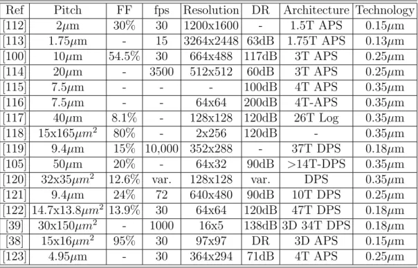
3.6 Recent CMOS Image Sensors . . . 35
3.7 Conclusion . . . 37
Chapter 4 CMOS IMAGE SENSOR ARCHITECTURE AND DESIGN CON-SIDERATIONS . . . 39
4.1 Why CMOS? . . . 39
4.2 Why a Digital Pixel Sensor? . . . 40
4.3 Why the CMOS 90nm Technology? . . . 40
4.4 Pixel Architecture . . . 41
4.4.1 Photosensitive Element . . . 41
4.4.2 Photosensing Circuit . . . 45
4.4.3 In-Pixel Analog-to-Digital Converter . . . 48
4.4.4 In-Pixel Digital Memory . . . 53
4.5 Modes of Operation . . . 54
4.5.1 Single-Exposure Linear Integration . . . 55
4.5.2 Multiple-Exposure Linear Integration . . . 55
4.5.3 Enhanced Dynamic Range Logarithmic . . . 57
4.5.4 High-Speed Differential . . . 58
4.6 Overall Architecture Overview . . . 58
4.7 External Controller . . . 60
Chapter 5 IMPLEMENTATION AND RESULTS . . . 62
5.1 ASIC Implementation . . . 62
5.2 Printed-Circuit Board Implementation . . . 64
5.3 Controller Implementation . . . 65
5.4 Post-Layout Simulation Results . . . 65
5.4.1 Comparator . . . 66
5.4.2 Photosensing Circuit . . . 70
5.5 Experimental Measurements . . . 77
5.5.1 Comparator . . . 77
5.5.2 Shutter Leakage . . . 80
5.5.3 Test Setup Validation . . . 87
5.6 Experimental Results Discussion . . . 88
5.7 Conclusion . . . 89
Chapter 6 CONCLUSION . . . 93
References . . . 100
Appendices . . . 122
A.1 Schematic Implementation . . . 122
A.2 Verilog and Verilog-A Implementation . . . 122
A.3 Layout Implementation, Issues and Considerations . . . 123
A.3.1 Minimum Well Spacing . . . 123
A.3.2 Pixel Signals Routing . . . 124
A.3.3 Capacitance . . . 125
A.3.4 Buffers . . . 126
A.3.5 Shift Registers . . . 127
A.3.6 Chip Area and Number of Pads . . . 127
A.4 Test Module . . . 127
A.5 Other Layout Details and Considerations . . . 129
B.1 Custom PCB . . . 132
B.1.1 Power Supply . . . 132
B.1.2 Ramp Generator DAC . . . 132
B.1.3 Voltage Reference DAC . . . 133
B.1.5 Voltage Dividers . . . 133
B.1.6 Flexible Connections . . . 134
B.1.7 Comparators . . . 134
B.2 FPGA Board . . . 134
B.3 MATLAB . . . 135
C.1 Switched-Capacitor Comparator Architecture (CMOS 0.18µm) . . . . 137
C.2 Switched-Capacitor Comparator Simulations (CMOS 0.18µm) . . . . 138
C.3 Differential-Input Pair Comparator Architecture (CMOS 0.18µm) . . 139
C.4 Differential-Input Pair Comparator Simulations (CMOS 0.18µm) . . . 140
C.5 Differential versus Switched-Capacitor Comparator . . . 142
D.1 Antiblooming and Exposure Control . . . 145
D.2 Image Smear . . . 146
D.3 Image Lag (or Sticking) . . . 147
D.4 Resolution . . . 148
D.5 Sensitivity . . . 148
D.6 Readout Schemes . . . 149
D.7 Noise . . . 150
List of Tables
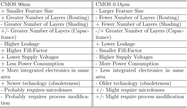
Table 2.1 Comparison between CCD and CMOS imagers . . . 24 Table 3.1 State-of-the-Art CMOS imagers . . . 35 Table 4.1 Comparison between CMOS 90nm and CMOS 0.18µm
Tech-nologies . . . 42 Table A.1 Capacitance Densities with Various Architectures . . . 126 Table A.2 Capacitance Extraction Simulation Results . . . 126
List of Figures
Figure 2.1 Pinned Photodiode . . . 8
Figure 2.2 Thin Film on ASIC . . . 9
Figure 2.3 Bayer Color Filter Array and Color Patterns . . . 9
Figure 2.4 Light responsivity of cones in the human retina . . . 10
Figure 2.5 Microlens Array . . . 11
Figure 2.6 Typical cross-section of a pixel with a color filter and microlens 12 Figure 2.7 Linear Array CCD Architecture . . . 14
Figure 2.8 Frame Transfer CCD Architecture . . . 14
Figure 2.9 Interline Transfer CCD Architecture . . . 15
Figure 2.10 PPS Architecture . . . 16
Figure 2.11 APS Architectures . . . 17
Figure 2.12 Common-Element APS Architectures . . . 18
Figure 2.13 DPS Architecture . . . 19
Figure 2.14 General example of a 3D-IC DPS pixel . . . 21
Figure 2.15 Image Noise . . . 26
Figure 2.16 Types of Noise in Image Sensors . . . 27
Figure 4.1 Photodiode Implementations . . . 43
Figure 4.2 Photodiode Biasing Configurations . . . 44
Figure 4.3 Photodiode Model . . . 45
Figure 4.4 Pixel Photosensing Circuit . . . 46
Figure 4.5 Switched-Capacitor Comparator Architecture (CMOS 90nm) . 50 Figure 4.6 3T 1-bit Memory Cell . . . 53
Figure 4.7 5T-Memory Cell Architecture . . . 54
Figure 4.8 Linear Integration Mode Non-Concurrent Clocking Signals . . 56
Figure 4.9 Linear Integration Mode Concurrent Clocking Signals . . . 56
Figure 4.10 Multiple Exposure . . . 57
Figure 4.11 Logarithmic Mode . . . 58
Figure 4.12 Differential Mode Clocking Signals . . . 59
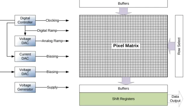
Figure 4.13 Overall Image Sensor Chip Architecture . . . 59
Figure 5.1 Pixel Layout . . . 63
Figure 5.2 Representative Circuit Layout . . . 64
Figure 5.3 Voltage Divider Simulation using Cadence . . . 65
Figure 5.4 PCB Routing using Mentor Graphics PADS . . . 66
Figure 5.5 Comparator Signals Simulation (Linear and Log Modes) . . . 68
Figure 5.6 Comparator Operation Simulation (Linear and Log Modes) . . 69
Figure 5.7 Comparator Simulation (Differential Mode) . . . 71
Figure 5.8 Logarithmic Mode Output Simulation . . . 72
Figure 5.9 Logarithmic Mode Output Simulation (Log Axis) . . . 73
Figure 5.10 Linear Mode Output Simulation . . . 74
Figure 5.11 Shutter Leakage Rectification Simulation . . . 76
Figure 5.12 Experimental Measurements of the Linear Mode Signals . . . 78
Figure 5.13 Comparator Experimental Measurements (Linear and Logarith-mic Modes) . . . 79
Figure 5.14 Multiple Exposures Mode Ramp and Shutter Signals Experi-mental Measurements . . . 81
Figure 5.15 Comparator Operation Experimental Measurements (Multiple Exposures Mode) . . . 82
Figure 5.16 Differential Mode Experimental Measurements . . . 83
Figure 5.17 Experimental Measurements of Follower Voltage on PD Resets 84 Figure 5.18 Experimentally Measured Follower Voltage while Ramping the PD Voltage . . . 85
Figure 5.19 Experimentally Measured Follower Voltage with Shutter Acti-vation . . . 86
Figure 5.20 Analog Ramp and Digital Ramp MSB Experimental Measure-ments . . . 87
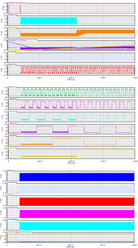
Figure 5.21 Experimentally Measured Clocking Signals . . . 90
Figure 5.22 Experimentally Measured PD Reset, Shutter and Voltage Di-vider Signals . . . 91
Figure 5.23 Experimentally Measured Supply Voltages and Oscillator Clock 92 Figure 6.1 Custom PCB Interfaced with Spartan-3 Development Board . 97 Figure A.1 Example of Mixed Simulation: Verilog, Verilog-A, Schematic . 123 Figure A.2 Pixel Layout . . . 124
Figure A.4 Representative Circuit Layout . . . 128
Figure A.5 Chip with Pads . . . 129
Figure B.1 Ideal Overall Test Setup . . . 131
Figure B.2 PCB Schematic . . . 136
Figure C.1 Switched-Capacitor Comparator (CMOS 0.18µm) . . . . 137
Figure C.2 Switched-Capacitor Comparator Worst-Case Corner Offset Sim-ulation . . . 139
Figure C.3 Switched-Capacitor Comparator Worst-Case Corner Simulation Memory Latching . . . 140
Figure C.4 Differential-Input Comparator (CMOS 0.18µm) . . . . 141
Figure C.5 Differential Comparator Offset Worst-Case Corner Simulation 142 Figure C.6 Differential Comparator Behavior Simulation . . . 143
List of Appendices
Appendix A Layout Implementation Details and Considerations . . . 122 Appendix B External Controller . . . 131 Appendix C CMOS 0.18µm Blocks . . . . 137 Appendix D Performance Parameters in State-of-the-Art CCD Image sensors 144
List of Notations and Symbols
3D-IC Three-Dimensional Integrated Circuit ADC Analog-to-Digital Converter
APS Active Pixel Sensor
BCCD Buried/Bulk-channel Charge-Coupled Device BPSG Boro-Phospho Silicate Glass
CAN Convertisseur Analogique-Num´erique CAPS Complementary Active Pixel Sensor CCD Charge-Coupled Device
CDS Correlated Double Sampling CFA Color Filter Array
CMC Canadian Microelectronics Corporation CMOS Complementary Metal Oxide Semiconductor CMY Cyan, Magenta, Yellow
CNA Convertisseur Num´erique-Analogique DAC Digital-to-Analog Converter
DPS Digital Pixel Sensor
DR Dynamic Range
DRAM Dynamic Random Access Memory DRC Design Rule Check
DSNU Dark Signal Non-Uniformity EHP Electron-Hole Pair
ESD Electro-Static Discharge FD Floating Diffusion FET Field Effect Transistors
FF Fill-Factor
FIT Frame Interline Transfer FPN Fixed Pattern Noise fps frames per second FT Frame Transfer
HDTV High-Definition Television ILT Interline Transfer
I/O Input/Output
IR Infrared
IT Interline Transfer
IT-CCD Interline Transfer Charge-Coupled Device JPL Jet Propulsion Lab
LSB Least Significant Bit LVS Layout Versus Schematic LWIR Long-Wave Infrared MBW Modified Barrier Well
MOSFET Metal-Oxide Semiconductor Field-Effect Transistor MSB Most Significant Bit
MiM Metal-Insulator-Metal MWIR Mid-Wave Infrared
NASA National Aeronautics and Space Agency NIR Near Infrared
PAPS Pseudoactive-Pixel-Sensor PCB Printed Circuit Board
PD Photodiode
PG Photogate
PGA Programmable Gain Amplifier PPD Pinned Photodiode
PPS Passive Pixel Sensor
PRNU Pixel Response Non-Uniformity PT Phototransistor
QE Quantum Efficiency
RAM Random Access Memory
RDS Reflection-Delayed noise Suppression RGB Red, Green, Blue
SCCD Surface-channel Charge-Coupled Device SNAP Shuttered-Node Active Pixel
SNR Signal-to-Noise Ratio SoC System on Chip
STI Shallow-Trench oxide Isolation SWIR Short-Wave Infrared
TDI Time-Delay-to-Integration TFA Thin Film on ASIC
TG Transfer Gate
V-CCD Vertical Charge-Coupled Device VHDL Very Highly Descriptive Language VLWIR Very-Long Wave Infrared
Chapter 1
INTRODUCTION
Image sensors have easily found their way into our everyday lives. They have become part of our daily routines ˆa sometimes without us being even completely aware of it. If you look around you right now, you would probably find a cell phone with an integrated camera lying on some table, a digital camera put away in a drawer, a webcam nonchalantly attached to your desktop computer or even a tiny camera integrated in the screen of your laptop. You leave your apartment, coming down the hallway a security camera is sending your picture to a control center to be relieved by another one in the parking lot of your building. You are backing out of your parking space, and the built-in sensor in your bumper shows you that you are getting too close to that dreaded pillar you had crashed into last time. You then stop at an ATM machine for some cash almost oblivious to the fact that you are getting your picture taken. You are finally on the highway, nothing in sight (or at least so you think), you get carried away and ˆaforgetˆa your foot on the accelerator; a few days later you receive a speeding ticket by mail... And this goes on and on... As a consequence, it goes without saying that the prevalence of image sensors in today’s society is beyond any shred of doubt. But are image sensors just associated with regular daily tasks and monitoring? The fact is that image sensors are just as important for consumer and professional applications as they are for industrial and medical applications amongst others. These applications vary from still imaging going through video imaging and attaining fast imaging.
For more concrete examples, it is quite tempting to mention some interesting applications in imaging. These could include Sony’s Dream Robot, Orange’s Mobile VideoPhone, Identix’s Fingerprint Scanner, Canesta’s Virtual Keyboard, Bendix’s IR Night Vision, Toyota Prius’ Self-Parking Car, Honda’s Lane Control, Given Imaging’s Wireless Endoscope Capsules, Suni Medical Imaging’s Digital Intraoral Camera ˆa and one of particular interest here: Polystim Neurotechnologies Laboratory’s Visual Cortical Stimulator. This project, dubbed Cortivision, is the intended application for
the image sensor which is the subject of this work.
The Cortivision project aims at creating an intra-cortical visual prosthesis to in-duce visual perception in blind patients by stimulating the visual cortex. Since the system bypasses the retina and the optic nerve, it might be ˆa unlike some of the other projects doted with the same humanitarian aim ˆa a viable solution for people who were born blind or have been blind for a lengthy duration leaving them with damaged retinas or optic nerves. The system to be conceived has certain criteria set in stone; two of which are its portability and the absence of wires or other obvious structures penetrating the cranium. This sets harsh limitations as to the dimensions, power consumption, and means of data transfer. The image acquisition module consists of a projector and an image sensor integrated on glasses ˆa each of them replacing one of the human eyes as per the principle of active stereoscopy. The acquired images are then transmitted to an external image processing module that intelligently selects pixels and shades of gray to create a 3D-feel for the patient. These are then wire-lessly transmitted to electrodes implanted in the brain to stimulate the visual cortex producing bright spots ˆa hereafter called phosphenes ˆa allowing the patient to have a good idea of the environment in which s/he is located endowing him or her with a certain extent of autonomy by allowing him or her to avoid obstacles and accomplish basic tasks without seeking the help of others.
The subject of this thesis is the image sensor which constitutes the frontend of the system and is an extension of the work started by Tr´epanier et al. [3]. As a result, it is to abide by the requirements set by the Cortivision application, while preserving the versatility that accompanies the possibility of it being used for other applications as well.
A question that may arise though: why design and implement our own image sensor and not just buy one off-the-shelf? Basically, our sensor is to be integrated in a complete portable system for our application ˆa so we need to have the possibility to integrate on it as much control circuitry and as much of the image processing circuitry as possible to make the whole processing the quickest possible, the least power consuming possible, and with the least possible area overhead. Part of the processing is already sped up and simplified by a special mode of operation of our sensor, the differential mode (which is actually a difference mode), that subtracts two consecutive image captures.
range is a necessity ˆa this would allow the capture of feeble as well as strong light signals in the same image. To boost the dynamic range, a logarithmic mode of operation is implemented along with the regular linear mode of operation. Another important constraint is the frame rate. The image processing module requires the capture of 20 images to generate a single processed image. Therefore, if we aim at having a final system having a rate of 20 images per second (to rival the human eye), we are required to have an image sensor that can deliver images at a rate of at least 400 frames per second (fps). Furthermore, the portability of the finished system imposes minimal possible dimensions and power consumption. Also, many particularities inherent to the CMOS 90nm technology have led to its adoption for the implementation of the Cortivision image sensor. These include, but are not limited to, reduced feature size (hence reduced area) and the novelty of this technology in image sensor research. This is while bearing in mind that smaller technologies (even 65nm) are being used by the image sensor industry, but are yet to appear in academic research mainly due to the higher cost of these, decreased availability and design overhead. Moreover, industrial research is in its greater part confidential and not accessible to scholars.
The first chapter will discuss the fundamentals of electronic image sensors. The second one will highlight some of the state-of-the-art work in CMOS image sensor research. Chapter 3 will describe the adopted architecture, and Chapter 4 will deal with the implementation, issues faced, and discuss any possible future improvements or suggestions. Details that might be of lesser impact to the reader have been placed in the Appendices.
Chapter 2
FUNDAMENTALS OF
ELECTRONIC IMAGE SENSORS
Conventional film photography is one of the most eminent and prevalent technologies with lots of applications. It is a chemical process that transduces light into a physical image through a series of reactions. Electronic imaging provides an alternative to this chemical technology by employing image sensors to transduce light into electrical signals which expands the applications due to the ease bestowed upon the processing, storage and transmission of electronic images.
The basic operation of an electronic image sensor can be summed up as the col-lection of photons, the generation of charges, the colcol-lection of these charges, their conversion into an electrical signal, the readout of this signal and finally the process-ing of what has been read out. In a nutshell: the conversion of optical signals into exploitable electrical signals.
2.1
Photosensing Principles
A sensor typically consists of a two-dimensional array of pixels. Each of these pixels contains a photosensing element. The portion of the pixel sensitive to light is mea-sured by a percentage called the Fill-Factor (FF). A good start for understanding electronic imaging, is acquiring basic insight into the behavior of charge carriers in semiconductors. An idiosyncrasy of semiconductors is that both electrons and holes act as mobile charges as opposed to only electrons in conductors. Light photons may be absorbed and hence make their way through the semiconductor. The absorbed energy induces the shift of electrons creating holes [4]. Each photon reaching the photosensitive element may generate one or no electron in the silicon, which in turn may or may not be collected by the pixel [5]. The efficiency of the conversion of received photons to free electron-hole pairs (EHPs) (that give rise to a photocurrent)
is denoted by the Quantum Efficiency (QE) of the detector [6].
QE = N umber of f ree EHP s generated and collected
N umber of incident photons (2.1)
This puts in perspective one of the main evaluation criteria of photodetectors: light sensitivity (which is also wavelength-dependent). The absorption coefficient of the photosensing element is an indicator of its sensitivity [4]. The photon absorption process for photogeneration, i.e. the creation of EHPs, necessitates a photon energy superior to the bandgap energy Eg of the semiconductor material to supply enough
energy for an electron to leave its valence band [6]. The bandgap energy, which is a property of the material, is also inversely proportional to the wavelength of the incident light. Hence, for greater wavelengths, the bandgap energy is lower, and the sensitivity higher since more photons can be detected [4]. This sets an upper cut-off wavelength (or threshold wavelength) λg for absorption [6].
λg =
1.24 Eg
(2.2)
For silicon, Eg = 1.12eV which yields a threshold wavelength of λg = 1.1µm. This
means that silicon photodetectors can be used for light in the visible spectrum, i.e. around 380nm to 750nm. As for sensitivity to the infrared spectrum, Miller [7] devised a scheme for dividing the band based on the response of various detectors:
? Near Infrared (NIR) [0.7µm - 1.0µm] ? Short-Wave Infrared (SWIR)[1.0µm - 3µm] ? Mid-Wave Infrared (MWIR) [3µm - 5µm] ? Long-Wave Infrared (LWIR) [8µm - 12µm]
? Very-Long Wave Infrared (VLWIR) [12µm - 30µm]
This means that NIR light can be detected by silicon (which is usually the part of the band used for imaging), and it “filters” out as well interference from other infrared light; for e.g. optical communication which typically uses wavelengths between 1.3µm and 1.5µm [7]. This makes it very suitable for our application where we would like to project and capture patterns of infrared light invisible to the human eye, yet without interfering with existing radiation.
Another important factor in photodetectors is the responsivity. It is defined as the ratio of the generated photocurrent density to the optical power per unit area
of the light; i.e. the electric output to the optical input [4]. So basically, greater photocurrents for lesser optical power beget enhanced responsivity. Responsivity at a given wavelength is given by [6]
R = P hotocurrent(A)
Incident Optical P ower(W ) = Iph
Po
(2.3)
For larger pixels, the FF is larger as well. This increases the number of photons that can be collected; however, this decreases the number of pixels in a given area, hence the number of devices on a wafer, which in turns boosts the production cost. Therefore, an important compromise in pixel design is pixel pitch versus FF to achieve a good photoresponse.
Several types of silicon-based photosensing elements exist, the most prominent of which are photoconductors, phototransistors (PTs), photogates (PGs), Thin-Film on ASIC (TFA) and photodiodes (PDs).
2.1.1
Photoconductors
They are the most basic type of photodetectors consisting of a semiconductor with ohmic contacts. Absorbed photons generate electrons and holes increasing the con-ductivity of the material, hence increasing the current flowing for a constant applied voltage bias. The gain is defined as the change in current with respect to the primary photocurrent. Photoconductors are distinguished for their high gain, but this comes at the expense of slow response and high noise [4].
2.1.2
Phototransistors
As a notion, all transistors are sensitive to light and can be used as photosensing elements. In practice, however, the narrow channel of Field Effect Transistors (FETs) drastically limits their responsivity - which is why bipolar transistors are favored over PTs. A large collector-base junction area is required to increase the number of photons collected and hence the sensitivity. Nevertheless, this results in a slower response speed [8]. Since our application requires a high frame rate, response speed is an issue, and bipolar transistors are not as readily available as FETs - noting that a combination of both requires special processing and additional expenses - which swayed the balance towards other photosensing elements.
2.1.3
Photogates
A PG is a MOS capacitor with a top plate formed of polysilicon. Consequently, it transduces optical signals into charges as compared to voltages and currents for the other semiconductor photosensing elements. These charges would then have to be transformed using other components into voltages or currents to become useful. The transfer of charges generates thermal noise due to the conductance of the transfer channel [8]. This makes it less appealing to us.
2.1.4
Photodiodes
The advantage of the PD as compared to other photosensing elements is mainly the ease of fabricating it in the inexpensive and widely available CMOS technology. It basically consists of a PN junction. Light generates electron-hole pairs that move to the N and P regions of this junction. Some of these carriers diffuse into the depletion region and are swept from the junction by the electric field prevailing in that region. The holes then move towards the anode and the electrons head towards the cathode generating a photocurrent or photovoltage that will be used to determine the incident light intensity. A thicker depletion layer increases the number of absorbed photons. To widen the depletion region, a reverse-biased configuration is opted for; however, this decreases the response speed [4]. Nevertheless, the response speed of PDs remains superior to that of the other photosensing elements and they remain the easiest to implement using a standard CMOS process because of their simple topology [9].
2.1.5
Pinned Photodiodes
The pinned photodiode (PPD) is more promising that both the PD and the PG. It provides a solution to the fact that a standard PD cannot be fully depleted upon readout, which creates image lag and FPN. In a PPD, the N-P structure of a regular PD is traded in for a P-N-P one as shown in 2.1. This structure allows the N- region to be fully depleted while there are still holes in the uppermost P region eliminating lag and FPN while preserving responsivity [10]. The voltage is then “pinned” to a fixed value.
PGs and PPDs both offer charge transfer from a large collection area of large capacitance to a small FD capacitance, but the QE of PPDs is far superior and require
Figure 2.1 Pinned Photodiode
less control signals than PGs aside from the fact that PGs require additional care to reduce leakage currents, which is intrinsic in PPDs. Nevertheless, PPDs require special process adaptation. Furthermore, as is the case for PDs, the PPD does not allow true CDS and the decrease of supply voltages with the newer technologies make it harder to have a pinned voltage while keeping enough head room for integration [11].
2.1.6
Thin Film on ASIC
TFA is basically the placement of the PD on top of the circuitry by a special tech-nique as illustrated in Figure 2.2, with the rear electrode connected to the circuitry underneath, hence creating a 100% FF. The QE varies typically between 60% and 80% depending on the wavelength in question [11]. Another advantage of TFA is that it can be used with any process generation, and that the optical problems introduced by stacking several layers with newer processes are avoided, nevertheless, capacitive coupling becomes an issue [11].
2.2
Color Imaging
We have seen in the Section 2.1 that Silicon PDs are sensitive to a certain range of light wavelengths. This means that they cannot differentiate between different colors. Typically, to circumvent that, a Color Filter Array (CFA) is placed on top of the pixel array. Each pixel would thus become sensitive solely to the wavelength
Figure 2.2 Thin Film on ASIC
that can traverse the filter on top of it. An algorithm is then used to recombine the gathered data and to produce a colored image.
Primary or complementary color filters can be used. The former imply the use of red, green and blue (RGB) filters while the latter make use of cyan, magenta and yellow filters (CMY). White filters can also be used in conjunction with color filters to measure the luminance signal [12].
One of the most popular filter configurations is the Bayer filter featured in Figure 2.3. People are more sensitive to high spatial frequencies in luminance (which contains the brightness information of the image) than in chrominance (that contains the color information of the image), and luminance is composed primarily of green light.
Therefore, the Bayer CFA improves the perceived sharpness of the digital image by allocating more spatial samples to the green image record [13]. Being an RGB filter, this is why it has two green filters for each red/blue pair. This way the filter better depicts the human retina that is more responsive to green as shown in Figure 2.4.
(a) (b)
Figure 2.4 Light responsivity of cones in the human retina: (a)[14], (b)[15]
Concurrently, another popular filter is the complementary mosaic pattern that has equal proportions of magenta, green, yellow, and cyan sensitive photosites arranged in magenta-green and yellow-cyan rows. It provides an improved image SNR (Signal-to-Noise Ratio) at low illumination levels relative to RGB patterns, as the sensor output signal level is much higher. However, the RGB patterns normally provide a better image SNR at higher illumination levels [13].
Patterns are thus built for each color, as shown in Figure 2.3 for the RGB in the Bayer CFA. An interpolation is then applied to find the color values in the intermedi-ate pixels. Many algorithms exist for that which is another very extensive topic that I shall not delve into.
Another interesting method that has more recently been put forth takes advan-tage of the fact that different wavelengths have different absorption depths in silicon. Longer wavelengths penetrate deeper. As a result, a vertical pixel can be constructed so that the RGB information can be collected at the same location in the 2D im-age plane but at different depths eliminating the need for filters and interpolation algorithms [16].
2.3
Lenses and Microlenses
The use of a lens to concentrate the light emanating from a scene on the image sensor is necessary to achieve a meaningful image. A typical camera lens system comprises several lenses redirecting the light in such a way as to recreate the image the most accurately possible on the image sensor while minimizing artifacts the likes of loss of contrast, blurring, distortion, etc.
Several parameters have to be taken into consideration in selecting a lens. The focal length determines the angle of view. A smaller focal length implies a wider angle of view and less susceptibility to image deterioration due to the shaking of the camera. Longer focal lengths require shorter exposure times to minimize blurring. Another important parameter of lenses is aperture. The aperture range indicates how much the lens can open up or close down to increase or decrease the amount of light reaching the sensor. Aperture is measured with an f-number (e.g. f/1.4). Lower f-numbers correspond to larger apertures and thus “faster” lenses because the shutter speed can be increased to obtain the same exposure [17].
On a slightly different note, having discussed photosensing and photosensitive elements, it is obvious that it is much coveted to increase the size of the photoreceptive area. One way of doing that without enlarging the pixel size is by employing microlens arrays. Figure 2.5 shows an example of such an array.
The microlens would focus the light on the photosensitive region of the pixel. This
can double or triple the fill-factor for CMOS image sensors raising it from a typical 20 to 30% to a much more desirable 70 to 80% [5]. Several methods can be used to create such arrays, from polymer-thin film [19] to etching glass [20] that is placed on top of the image sensor to even more innovative methods such as a process of surface tension and injection [18].
Figure 2.6 shows a typical cross-section of a pixel with a color filter and microlens. The photodiode occupies a portion of the pixel. The remainder of the pixel is covered by a metal shield to prevent light from interfering with the circuitry underneath it. The color filter is on top of the sensor and a microlens concentrates the incident photons on the photodiode covered by the filter. Nevertheless, I shall not delve any deeper into this topic since it is beyond the scope of this thesis.
Figure 2.6 Typical cross-section of a pixel with a color filter and microlens
2.4
Electronic Image Sensors
The two basic types of electronic image sensors available nowadays are Charge-Coupled Devices (CCDs) and CMOS (Complementary Mos Oxide Semiconductor) image sensors. CCDs have long been established as a technology for image sensors, however, CMOS image sensors surfaced after that offering several advantages com-pared to CCDs; namely the possibility of lower power consumption, higher frame rates, use of existing technology processes and incorporating circuitry on the image sensing chip which meant lower costs and greater integration potential. A battle
thus erupted between the proponents of CCDs and CMOS image sensors. A lot of people were drawn to the potential of CMOS sensors by mere curiosity despite their being uncertain of the benefits. This led to a lot of experimentation but also to a distorted market behavior where a lot of greedy startups went bankrupt: a lot of peo-ple were investing in CMOS sensors “blindly” [21] and CMOS imagers were at first priced below their cost to win business [22]. The battle cooled off around 2002 and took on a more realistic turn based on cash-flow and not on capital investment in a “new technology” that sparked curiosity. Nevertheless, the sudden interest in CMOS sensors did have some advantages in making it a norm in a lot of applications such as video-conferencing, desktop and barcode scanners, etc [21]. The current market focuses more now on long-term consumer stability than on high-risk startups [22].
2.4.1
CCD Image Sensors
CCDs saw the light of day in 1969 at the Components Division of Bell Labs with Drs. Willard Boyle and George Smith. This was the dawn of digital photography [23]. CCDs are basically arrays of photosites with charge collecting buckets that can transfer their charges to each other [23]. These “buckets” are actually capacitors con-nected together that can transfer their charge to and receive charges from neighboring capacitors via voltage control. MOS capacitors are typically used in such cases. Each consists of a gate above a silicon oxide layer in a p-type silicon substrate. When a positive voltage is applied to the gate, a depletion region is formed under the silicon oxide layer causing electrons to accumulate. These electrons can then be transferred to neighboring capacitors by changing the gate potentials. This makes charges among the capacitors coupled, hence the origin of the name of this type of sensors.
Since silicon has a bandgap energy of around Eg = 1.12eV , and pertaining to
the discussion in Section 2.1, the silicon substrate can readily absorb photons if they have sufficient energy and if they hit the silicon, preferably at the depletion region. This generates EHPs and the number of electrons accumulated in the depletion well becomes proportional to the number of absorbed photons. This makes it possible for CCDs to take on the role of image sensors [12].
CCDs shift electrons through stages to an output amplifier. Relatively high volt-ages are required to be able to pull the electrons between stvolt-ages. They are usually directed to a single amplifier at the corner of the array and an analog video signal is
outputted. Shifting can nevertheless cause image blurring, which is why light shields should be used [5]. CCD sensors can roughly be classified into three architectures.
The first is the linear array architecture shown in Figure 2.7. The charges from each CCD are transferred to a shift register that then redirects them to an output amplifier. This type of architecture is common in scanners where the possibility of using low-cost high-resolution linear arrays exists [12].
Figure 2.7 Linear Array CCD Architecture
The second architecture is the Frame Transfer (FT) one [5; 12] featured in Figure 2.8. In this case, the entire CCD image is shifted vertically into an identical shielded CCD. This, however, results in a large smear since it takes around a millisecond to transfer the image [5]. FT sensors have high FFs of 100%, but suffer from slow readout rates [12].
Figure 2.8 Frame Transfer CCD Architecture
The third architecture is the Interline Transfer (ILT)[5; 12] one portrayed in Fig-ure 2.9. In this architectFig-ure, each pixel has its own diode and shielded storage and
transfer area. This, nevertheless, results in a decrease in FF, which can be, how-ever, compensated by using microlenses [5] as discussed in Section 2.3. The low FF attributed to this architecture is counterbalanced by a fast readout rate though [12].
Figure 2.9 Interline Transfer CCD Architecture
Combinations of these architectures also exist. One of these is Frame Interline Transfer (FIT)[5; 12] which reduces smear. Nevertheless, it should be noted that the FT and FIT architectures both entail an increase in die size and hence an inevitable increase in cost [5].
When it comes to refinement, CCDs are well-renowned for their excellent image quality and output uniformity. The CCD process is acclaimed for its high fidelity; nevertheless, this comes at an increase in cost. The high image quality standards also come at an increase in power consumption to be able to decrease noise. This is also partially due to high clocking voltages, typically between 2.5V and 10V, and the need for multiple supply and biasing voltages. Another drawback is the sequential readout which contravenes the attainment of higher frame rates [23] and window-of-interest readout without the risk of charge overflow. Furthermore, no other circuitry (e.g. ADCs or clocks) can be added to the sensor chip since they would contribute to substrate noise. Therefore, a set of chips is needed which makes miniaturization harder [5].
Regardless, CCDs are very well-established. They have been around and have evolved for close to 40 years, so CMOS sensors do have quite a challenge to overcome if they want to replace CCDs - so they better have something astounding to offer to make them stand out.
2.4.2
CMOS Image Sensors
CMOS image sensors have evolved over the last decades. The first CMOS image sensor was the Passive Pixel Sensor (PPS). The pixel consisted of a photodiode and an access transistor [24] as shown in Figure 2.10. As a consequence, it had a very high fill-factor. However, the signal quality was poor and the analog-to-digital voltage conversion time increased with the number of pixels because the architecture had a single external ADC common to all pixels. PPSs were offered by Reticon starting in the late 1960s. Their use in camcorders was tackled by Hitachi and Matsushita in the 1980s [25]. Nonetheless, Peter Denyer was the first to implement a PPS with substantial integrated electronics in 1991 describing it as “extending the CMOS ASIC marketplace in a sector of high growth rates” which is image sensing. This sensor had a matrix of 312 x 287 pixels, with pixel sizes of 19.6µm x 16µm. Each column had a sense amplifier and pixels could be addressed and shifted out via an output amplifier as the last stage [26]. Denyer then went on to establish a company VLSI Vision to commercialize this sensor in 1990. His company was acquired by STMicroelectronics in early 1999, becoming their Imaging Division, and continues to produce CMOS image sensors [27]. For these sensors, wire capacitance is an issue. This makes them less scalable and less enviable in high rate applications for as capacitance increases and speed increases, noise increases as well [25], making their advantages of high fill-factor and small pixel size take a backseat.
Figure 2.10 PPS Architecture
An improvement over the PPS was the Active Pixel Sensor (APS). The original APS was developed by Noble in 1968 [28]. For the APS, a follower was added inside
each pixel, as delineated in Figure 2.11(a) thus improving the signal quality - rivaling CCD quality. However, no improvement was brought upon the conversion time [29]. So basically, each pixel has its own amplifier to create a charge gain between the photodetector and the analog signal at the bottom of each column. The in-pixel amplifier is typically a source follower due to its simple configuration and uniform gain. This makes the sensor less susceptible to noise at an expense of a decrease in fill-factor. The first real advocates for it were researchers from the National Aeronautics and Space Agency’s (NASA’s) Jet Propulsion Lab (JPL), namely E.R. Fossum [25]. The initial goal of JPL while developing their APS CMOS image sensor was to get an image sensor that consumes less power and that is less susceptible to radiation damage in space [23]. They founded Photobit Corp. that commercialized the first APS-based systems [25]. It was purchased by Micron in 2002 that combined Photobit’s imaging design technology with its own DRAM process [30].
(a) (b)
Figure 2.11 APS Architectures: (a) 3-Transistor, (b) 4-Transistor
APSs are very common in today’s research and industry. Several architectures for APSs have been developed over the years. The original configuration was a 3-Transistor one as the one featured in Figure 2.11(a). It basically consists of a pho-todiode, a reset transistor, a source follower and a row select transistor. The diode is initially reset to a high voltage and is then left to integrate decreasing the voltage across the diode as the photons are absorbed and converted to charges. Disadvantages of this architecture are typically that the sense node where the diode and reset tran-sistor meet incurs an elevated dark current contributing additional noise. Moreover,
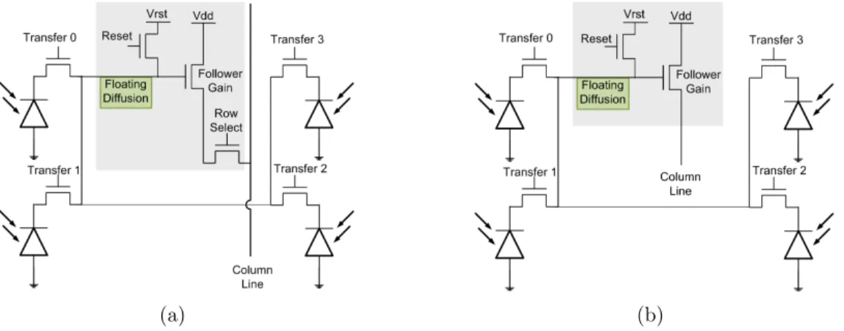
the output response is non-linear because the capacitance of the photodiode depends on the voltage affecting the charge-to-voltage conversion as the diode fills up. Fur-thermore, residual charge on the photodiode can create ghost images in fast-changing light settings [31].
An alternative APS architecture is shown in Figure 2.11(b) where 4-Transistors are used in each pixel. A transfer gate is added to separate the photodiode from the floating diffusion. In this case, a reset implies the activation of both the reset and transfer transistors applying a high voltage to both the diode and the floating diffusion. Next, the transfer gate is disconnected and the diode is left to integrate. Prior to measurement, the reset transistor is activated again to reset the floating diffusion only this time. Afterwards, the transfer gate is activated to transfer the charge from the diode to the floating diffusion. This design permits true Correlated Double Sampling (CDS) (see Section 2.4.4) since the same reset level is used to measure the reset value and the signal value [31]. Several other APS architectures have appeared in the literature that have common-element or shared configurations. Figure 2.12(a) shows a 1.75T architecture. It is basically a readaptation of a 4T architecture where four pixels share the same floating diffusion, reset gate, source follower and row-select transistor. Nevertheless, each pixel still has its own transfer gate that should be activated one at a time to read out the values at the photodiodes. An even greedier architecture is the 1.5T architecture shown in Figure 2.12(b). It is similar to the 1.75T architecture but eliminates an extra transistor: the row-select
(a) (b)
Figure 2.12 Common-Element APS Architectures: (a) 1.75-Transistor, (b) 1.5-Transistor
one. By doing this, however, the readout strategy is modified. We no longer read out row by row.
Instead, the reset voltage and Vdd of the pixel are sent as pulses to be able to turn the follower transistor on and off to give or deny access to the column bus. The readout strategy also involves reading out blocks of pixels and separating even columns from odd ones to be able to multiplex the values on the signal buses. Details can be found in [32]. A 1.25T pixel is also achievable by having two blocks of four pixels arranged in parallel that share a readout and reset transistor [33].
Despite the good performance of APSs, they are still not as sensitive as CCDs: light may land on transistors, the gain is lower and the noise greater [23].
The most recent architecture is the Digital Pixel Sensor (DPS) depicted in Figure 2.13. The first DPS was developed by El-Gamal at Stanford University around 1994 [34]. The DPS integrates an Analog-to-Digital Converter (ADC) within each pixel along with a digital memory. This allows parallel conversions to occur in each pixel making the conversion time independent of the number of pixels (not to be confused with the readout time). This however is done at the expense of a decrease in fill-factor since more circuitry is added to each pixel. The incorporation of an ADC in each pixel allows for massively parallel conversion, very high-speed readout and
greater Dynamic Range (DR) [29]. DPSs are particularly interesting since they have more potential for higher frame rates and since with the new design technologies, the dimensions of transistors are becoming smaller and smaller lessening the impact on the fill-factor and making it less overwhelming.
To wrap up this section on a slightly different note, an interesting approach has lately been introduced into the image sensor world due to the advent of 3D-ICs (Three Dimensional Integrated Circuits). These should not be confused with 3D packages that consist of different chips with different functions stacked inside a single pack-age and connected together [35]. A 3D-IC is a stack of multiple dies with direct connections tunneling through them. This reduces the interconnect length due to the key advantage of allowing wires to be routed directly between and through the wafers [36]. It is basically integrating planar device layers with short vertical in-terconnections. 3D interconnect boasts the advantages of decreased cost, improved performance and ameliorated integration [37]. The main drawback, however, is that area enough for thousands of transistors is sacrificed. Nevertheless, this waste in area can be somehow compensated by smart placement and routing strategies to use these vacant areas for through-hole wiring [36]. Image sensors that use this technology usu-ally place the different modules of the sensor on different layers or “tiers” with the uppermost tier having the photosensing element with minimal circuitry to improve the fill-factor making it very close to 100%. Figure 2.14 shows a generalized example of a DPS pixel with the first tier containing the photosensing circuit, the second the ADC and the third the digital memory. The layers are connected together with vias. This reduces the overall area of the sensor and minimizes parasitics as well by short-ening traces. Several 3D-IC image sensor architectures have been brought forth the likes of [38] and [39].
2.4.3
CCD vs. CMOS Image Sensors
The companies that manufacture image sensors can be divided into four groups each favoring a specific technology being CCD or CMOS. Japanese electronic firms - such as Sony, Matsushita and Sharp - tend to have an inclination towards CCDs, while semiconductor suppliers and foundries - like Agilent, TSMC, UMC and ST - along with fabless suppliers - namely Omnivision - are advocates of CMOS sensors. Estab-lished companies in the image sensing field - the likes of Kodak, Canon, Dalsa and
Figure 2.14 General example of a 3D-IC DPS pixel
Fujifilm - tend to have both [40]. So this is enough to see that both image sensing technologies are widely spread and extensively commercialized. The overpromotion of both CCD and CMOS sensors and the relentless battle between them have engen-dered a lot of fear, doubt and uncertainty in the domain of image sensors. As Dalsa puts it, it is much like comparing apples to oranges: both can be good for you [22]. So essentially, depending on ones needs, s/he would sway towards one or the other.
The concepts of both CCD and CMOS image sensors have been around since the late 1960s, early 1970s. Nevertheless, CMOS image sensors took a longer time to emerge since the CMOS technology was not mature enough at that time to allow CMOS sensors to compete with CCD ones. Feature sizes were not small enough and process uniformity was left to be desired. That was true until the 1990s when CMOS technology flourished and there was revived interest in CMOS image sensors: they were proponents of integration, miniaturization, portability, low-power consumption, low defect and contamination levels and low fabrication cost since they used already-existing processes with new circuit techniques adapted from CCDs to achieve low noise and high DR. However, some unexpected surprises were waiting around the corner: design time was greater, quality was inferior and even the cost was higher since process adaptations turned out to be necessary to achieve certain image quality standards [22; 5]. The following discussion compares some of the issues faced by the two imager types.
An important factor when dealing with CCDs is Antiblooming. In general, bloom-ing occurs when the full-well capacity of the pixel is exceeded, causbloom-ing charges to overflow into adjacent pixels. This is usually addressed by biasing the region around
the cells during integration [41] or adding an overflow CCD to contain the superfluous charges that would then be transferred to an output and eliminated [42]. This problem is not intrinsic to CMOS imagers - what one might mistake for “blooming” in CMOS sensors is usually caused by Image Lag or Sticking. Image lag/sticking/ghosting oc-curs when there is an improper reset or improper/incomplete charge transfer. A residue of the previous image would appear in the current frame, and perhaps addi-tional subsequent frames creating a “ghost”. This can be observed in both CMOS and CCD imagers. Another important similar phenomenon is Image Smear. In general, image smear occurs when charges are shifted (CCDs) or with rolling shutters if the image scene is non-stationary (CMOS).
Resolution is one of the first parameters that one inquires about when buying a sensor. Increasing the resolution was one of the greatest initial goals in image sensor design. Nevertheless, such sensors had to overcome certain obstacles to become practical. Basically, the resolution increase if not matched by a photosensitive area increase, impairs the sensitivity of the sensor [43]. CMOS pixels usually have a smaller fill-factor (percentage of the pixel sensitive to light) which can be 20% or less because they have circuits integrated in them [44] while it is close to 100% for CCDs [22]. However, putting sensitivity on the side, CCD and CMOS imagers have an identical response to light collection of photogenerated electrons [5], which makes the most notable differences between them the charge-conversion and readout techniques. In CCDs, charge is transferred from pixels to a common element to convert them to voltages and send them off the chip serially [45] as a single output analog signal [22]. For CMOS sensors, the charge to voltage conversion is done within each pixel and the voltages are transferred out of the pixels instead [45] to be read out like in a RAM (Random Access Memory) with column and row addressing circuits.
One of the essential contributors to image quality is dynamic range (DR) which is defined as the ratio of the saturation level of the pixel to the signal threshold [45]. In simpler terms, it is the ability of the sensor to differentiate between very low and very high light intensities in the same image thus preserving the details in both the dark and bright areas of the image [46]. Here, CCDs are better due to their lower noise because of their quieter substrates [45]. However, CMOS imagers offer better SNR and DR at higher rates [23]. They allow high-speed readout and hence higher resolutions [29]. This strength comes mainly from their parallel output structure [22] and the integration of all the functions on the same chip making them popular in
![Figure 2.4 Light responsivity of cones in the human retina: (a)[14], (b)[15]](https://thumb-eu.123doks.com/thumbv2/123doknet/2331439.31786/35.918.208.781.288.582/figure-light-responsivity-cones-human-retina-b.webp)

![Figure 2.15 Image Noise: (a) Original, (b) Random noise [48], (c) Pattern noise [49]](https://thumb-eu.123doks.com/thumbv2/123doknet/2331439.31786/51.918.173.801.167.391/figure-image-noise-original-random-noise-pattern-noise.webp)