HAL Id: hal-02492270
https://hal.archives-ouvertes.fr/hal-02492270
Submitted on 26 Feb 2020HAL is a multi-disciplinary open access
archive for the deposit and dissemination of sci-entific research documents, whether they are pub-lished or not. The documents may come from teaching and research institutions in France or abroad, or from public or private research centers.
L’archive ouverte pluridisciplinaire HAL, est destinée au dépôt et à la diffusion de documents scientifiques de niveau recherche, publiés ou non, émanant des établissements d’enseignement et de recherche français ou étrangers, des laboratoires publics ou privés.
Study of suitable dielectric material properties for high
electric field and high temperature power semiconductor
environment
Marie-Laure Locatelli, Karine Isoird, Sorin Dinculescu, Vincent Bley, Thierry
Lebey, Dominique Planson, Michel Mermet-Guyennet, E. Dutarde
To cite this version:
Marie-Laure Locatelli, Karine Isoird, Sorin Dinculescu, Vincent Bley, Thierry Lebey, et al.. Study of suitable dielectric material properties for high electric field and high temperature power semiconductor environment. 10th European Conference on Power Electronics and Applications (EPE’2003), Sep 2003, Toulouse, France. �hal-02492270�
Study of suitable dielectric material properties for high electric field and
high temperature power semiconductor environment.
LOCATELLI M.L., ISOIRD K.
(1), DINCULESCU S., BLEY V., LEBEY T.,
PLANSON D.
(2), MERMET-GUYENNET M.
(3), DUTARDE E.
(3)Laboratoire de Génie Electrique de Toulouse – UMR CNRS 5003
Université Paul Sabatier, bât. 3R3
118, route de Narbonne
31062 Toulouse, France
Tel : 33 (0)5 61 55 67 12/Fax : 33 (0)5 61 55 64 52
[email protected]
(1)
Adresse actuelle : Laboratoire de Micro-électronique de Puissance
- 7 avenue Marcel Dassault – 37 204 Tours, France
(2)
Centre de Génie Electrique de Lyon – UMR 5005
INSA Lyon, bât. 21 – 20, avenue Albert Einstein - 69621 Villeurbanne, France
(3)
ALSTOM Transport
50, rue du Docteur Guignier – 65600 Séméac, France
Aknowledgments : BOULANGER A, FERRE P. and RENAULT D. for efficient technical support.
Keyword list : « Power Semiconductor Devices », « Silicon Carbide », « Simulation », « Device Characterisation », « Packaging », « Reliability »
Abstract
Due to more severe operating condition (higher electric field, higher temperature,…), power electronics trends require to consider more accurately the dielectric environment of the semiconductor. The use of possible alternative semiconductors adds reason for such studies. Maximum electric field stress, relative dielectric permittivity and energy band gap properties, theoretically required for the SiC device passivation, are discussed. Advantages and drawbacks of high dielectric permittivity materials for passivation are emphasized. Then, a new 50 kV / 500°C experimental set-up allowing their precise characterization once the test-vehicles chosen, is presented in the paper.
1. Introduction
A current trend in power electronics is to increase the integration level. The first main motivation lies in the reduction of these systems’ sizes (volume and weight). Such a reduction represents energy saving for their transportation and also space saving, exploitable for new capabilities. This increase in volumic power requires components presenting both lower power losses and a smaller system complexity (for example a lower number of discrete components per function). An increase in both system efficiency and reliability is expected, which constitutes the second significant source of interest. Indeed, the research for power system integration includes (but is not limited to) other trends of the power electronics : higher operation frequency (leading to the size reduction of filters, capacitors, self and inductive machines), higher junction temperature (for both a decrease of the cooling system size and an increase of the switched power density), and power devices able to withstand a higher voltage (to avoid component series association, or for a direct power conversion from the distribution networks).
Therefore, power devices are expected to endure more severe operating conditions. These new stresses on the device constitutive materials impose to reconsider at the same time the system concept, the component architecture, the manufacturing technology processes, or even the material nature when physical limitations are reached. We can mention works on novel silicon structures (ex: CoolMOS [1] , …), and on new semiconductors (silicon carbide, gallium nitride, diamond [2], …). These latter are
motivated by the silicon power devices limitations at high frequency (some kHz in railways applications) at high voltage (9 kV for rectifier diodes, 150 V for Schottky diodes) and at high temperature (ex: TJmax usually equals to 125°C (sometimes 140°C) for 3 kV to 6 kV fast switch
diodes). A wide band gap energy, together with a high critical electric field, a good electron mobility and a high thermal conductivity, are suited semiconductor properties for significantly rising up the power device limits, as already demonstrated by numerous SiC demonstrators (19 kV bipolar diode in SF6 gas [3], 2.6 kV-300°C on-wafer GTO [4]) and few commercial products (600 V-12 A-175°C
Schottky diode in TO 220-2 case [5]).
In the semiconductor die environment, the dielectric materials, and more generally speaking, the whole packaging elements, have to follow these changes. These materials endure stresses which are induced either by external causes (the system (f, V, T) operating conditions) or internal causes (related to the semiconductor part). Among them we focus on the SiC-component passivation layer. This paper presents simulation results performed to quantify the theoretical electrical stress that this passivation layer has to withstand. On the other hand, this approach leads us to deduce the main physical properties that this layer has to present. A 4H-SiC P+NN+ diode with Junction Termination Extension (JTE) periphery protection is considered in this study. Indeed, the planar JTE technique is often used, being efficient against premature breakdown of SiC devices ([3], [4], [6]).
Besides, since the interest in these new components is also their ability to operate in a higher temperature region than current ones, specific characterization means have to be built. The goal is to demonstrate the effective material abilities when high electric field and high temperature are applied at the same time. For this reason, an experimental set-up has been built allowing the measurements of material dielectric strength, or device breakdown voltage and leakage current, under voltage magnitudes and ambient temperatures up to respectively 50 kV and 500°C. This novel equipment principle, is presented in the second part.
2. Suitable material properties for the passivation layer of a SiC-component
2.1 Properties to be considered and method used for this study
Electric field distribution evaluation using two-dimensional finite element simulation
The first point to be considered is the increase in the electric field value (E) applied to the
semiconductor dielectric environment. When a wide band gap semiconductor is considered due to
its higher breakdown field (Ec), the die surrounding materials have to endure higher electrical stresses.
Indeed, to receive the highest system performance benefit for a targeted blocking voltage rating, the active device is designed to approach the maximum electric field value that the bulk of the semiconductor is able to withstand using the maximal doping level. Last, PN junction curvatures or interruptions, within the component or at its periphery, may create localized electric field reinforcement.
Maximum operating electric fields have therefore to be quantified in order to determine the lowest breakdown fields required for both SiC passivation and coating materials. The aim is to allow the maximal operating voltage of the whole structure to be as close as possible to the breakdown voltage of the semiconductor part (dimensioning concern), and to be stable versus time (reliability concern). For the present study, we focus our interest on the SiC device passivation layer, using the example of the 4H-SiC bipolar JTE-diode. The electric field stress impact on carrier injection at the interface between the passivation layer and the semiconductor die, has to be considered too, especially with an eye to increasing temperature operations. This second concern will determine the minimal band gap energy of the passivation layer material directly in contact with the semiconductor surface. The influence of εrP, the dielectric relative permittivity, for a given thickness of the passivation layer tP,
has been mainly investigated as an important factor for the E field repartition both inside and outside the semiconductor, and for the reliability concern.
In order to evaluate this electric field distribution within and outside the semiconductor, finite element
simulation method is applied, using MEDICI software [7]. It allows the description of the whole structure geometry under study, (including the semiconductor, the metallic electrode, the passivation
layer(s) and the insulating environment domains). The particular case of the P+NN+ diode considered
is presented in Fig. 1. After its geometrical description, the structure was meshed into finite elements to allow the calculation of electrical and physical quantities (like potential, electric field, charge carrier concentrations, current density, impact ionization rate, …) at each grid node. Due to the necessity to fix appropriate boundary conditions and to include the semiconductor environment, the structure to be simulated becomes quite large (even when taking into account the device symmetry). The difficulty resides in setting a fine enough meshing, providing correct results while keeping the total number of calculation points below the software limit (around 2x10⁴ points at maximum). In the studied case, the
chosen values for the extension of the epitaxy lateral margin (M=200 µm) and for the insulating environment thickness (t=100 µm) allowed an acceptable evaluation of the electric field distribution at the device sensitive areas.
The silicon carbide parameters were then provided for the physical models of the semiconductor region. The dielectric materials were declared as "insulator" regions, allowing to fix the dielectric permittivity parameter value (the other parameters, like electronic affinity, energy band gap, were kept equal to those of SiO2). Only the Poisson's equation was solved in these insulating regions. The
electrical resistivity of these insulating regions is considered infinite. No effective semiconductor surface charge was taken into account in this work.
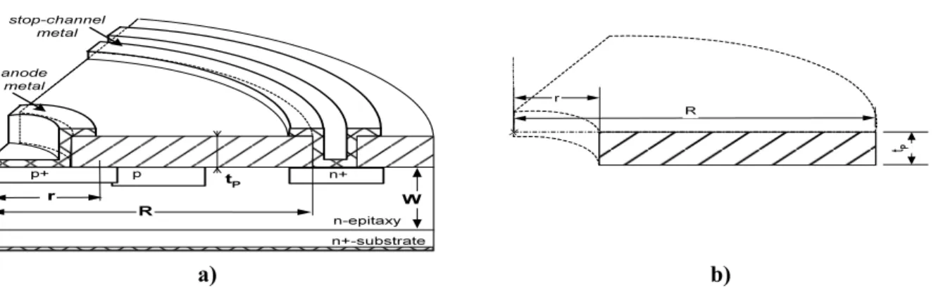
Fig. 1: Simulated high voltage P+NN+ 4H-SiC
JTE diode with 40 µm / 1.2×1015 cm-3
n-epilayer, 0.5 µm / 4×1019 cm-3 p+-implanted
emitter, 0.4 µm / 1×1013 cm-2 p-implanted JTE,
anode metal radius = 92 µm, emitter radius = 125 µm, JTE length L = 250 µm, epitaxy lateral margin M = 200 µm, simulated structure width = 565 µm.
The geometry and doping levels specified in Fig. 1 correspond to the "optimal" design of the [SiC, insulating environment] system, in absence of any passivation layer, leading to a maximal breakdown voltage of 5.75 kV. This breakdown results from the carrier generation by impact ionization into the semiconductor at the emitter junction curvature). This particular structure is used as a reference point, for studying the effect of inserting different kinds of passivation layers on the E field distribution, and for evaluating theoretical requirements on their main properties.
Passivation capacitance evaluation using analytical calculation
a) b)
Fig. 2: a) Example of device (a circular P+NN+ diode with stop-channel ring), and b) the equivalent
cylindrical capacitor used for the capacitance analytic calculation.
Fig. 2a) presents an example of structure where the passivation layer may act as a parasitic
capacitance C
Pin parallel with the semiconductor blocking junction. This case corresponds to
a P
+NN
+diode with the passivation layer connected between the P
+-anode metal and the N
+-stop-channel ring metal.
In order to evaluate the impact of this C
Pcapacitance on the dynamic operating performance
of the device, we considered that the passivation layer was equivalent to a cylindrical
capacitor (Fig. 2b), and the following equation was used for C
Pcalculation :
2.2 Results and discussion
Dielectric strength (EBrP) and relative permittivity (εrP) requirements for SiC device passivation
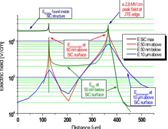
Fig. 3 presents an example of electric field lateral distributions at different altitudes near the semiconductor surface for the diode shown in Fig. 1, covered only with a t=100 µm / εr=1-insulating
environment, for the 5750 V reverse bias, which corresponds, in this case, to the SiC avalanche breakdown voltage.
Fig. 3: Total electric field lateral distributions at different altitudes near and outside the SiC surface of the structure presented in Fig. 1 (50 nm below, 50 nm above, 10 µm above), for Vbr=5750 V. The black curve indicates the
maximum electric field within the semiconductor part for each lateral X coordinate. This curve highest value is situated at the p+-emitter junction curvature
(X=+125 µm from the left, Y=+0.5 µm below the SiC surface).
As is shown in Fig. 3, one can observe first that the electric field distributions around the JTE-diode are strongly non uniform along an horizontal line.
The second observation arising from Fig. 3 is that the electric stress induced in this SiC diode environment can locally reach values close to 3 MV/cm. The E field maximum magnitudes outside the semiconductor are located close to the surface at the edge of the JTE. These values are about 10 times higher than the usual ones for Si devices, due to the fact that EcSiC critical electric field is
approximately 10 times higher than the Si one. It has to be noted that this enhanced stress occurs whatever the device voltage rating, so it is a common feature of all SiC structures. Moreover, using a higher EBr semiconductor (like diamond) would lead to a further increase of the above stresses,
reinforcing the interest of the study of the die environment. It should be added that the field peak at the edge can not be decreased by modifying the protection parameters, like increasing the JTE-length or depth (as checked by other simulations not shown here). Moreover, this peak magnitude being very close to the SiC critical avalanche field, the breakdown voltage of this kind of structure is very sensitive to the JTE doping process (a lightly higher doping level than the optimal value dramatically affects the breakdown voltage) [8].
From another hand, the table I gathers the critical electric fields given for different inorganic dielectrics already used or investigated as high relative permittivity (εr) gate dielectrics or secondary
passivant in Si technology. This table also presents the so called operating electric fields for few of these materials. Before trying to compare these data with the maximum E field values around the SiC JTE-diode, several remarks have to be done. First, the Ec critical field values given in Table I generally
correspond to the insulator dielectric strength measured using MIS (Metal Insulator Semiconductor) or MIM (Metal Insulator Metal) parallel plane configurations, and for a particular insulator thickness
(usually very thin for MIS applications). Also, the Eop operating field values (extracted from Lipkin et
al. [9]) are derived from MIS structure characterizations as well. They generally correspond to the maximum field within the insulator above which excessive leakage currents were experimented, often related to charge carrier injection either from the semiconductor or the metal gate.
Ec (MV/cm) Eop (MV/cm) εr Eg (eV) SiC-4H 2 9.7 3 SiO2 11 2 3.9 9 Si3N4 11 2 7.5 5.1 AlN 10-12 3 8.5 6.2 Al2O3 10 8.8-12 8.7 Ta2O5 9 0.3 24-26 4-4.5 HfO2 3-4 25 5.7 ZrO2 3-4 25 7.8 TiO2 6 0.2 40-80 3.5 BaTiO3 >150 3-4 polyimid 1.5-3 2.8-3.5 parylene 2.1-2.8 2.65-2.8
Table I: Critical electric fields, operating fields (extracted from [10]), relative permittivity and forbidden energy band gaps of commonly used or investigated materials for Si technology gate dielectrics or secondary passivation. Data come from [9], [10], [11].
So, the passivation dielectric stress is very different than the one of a MIS or MIM structure gate dielectric. In this last case, the electric field is uniform through the insulator, and normal to the interfaces with the semiconductor and the metal. Another important difference between these two dielectric configurations is the absence of the metal gate over the JTE-diode passivation zones where high E fields occur. Hence, no carrier injection from a metal can take place into the passivating dielectric. Moreover, the following results will point out the strong dependence of the electric field values in the JTE-diode environment on the relative permittivity (εrP) of the dielectric.
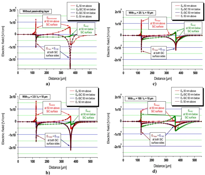
Fig. 4 presents the evolution of the distributions of the tangential (
E
T) and normal (E
N) components ofthe electric field, at both sides of the semiconductor surface, for the same SiC structure as in Fig. 1. Four different cases are considered: with the [t=100 µm / εr=1] insulating medium alone (idem Fig. 3),
with a [tP=10 µm / εrP=3.9] passivation layer, with a [tP=10 µm / εrP=25] passivation layer, and with a
[tP=10 µm / εrP=100] passivation layer. In all cases the passivant is covered by the same insulating
ambient. The simulator solves the Poisson's equation alone in these cases, for the same 5750 V as in Fig. 3. N.B. : the theoretical continuity of the ET component at the interface between two different
materials can be checked in Fig. 4 ( (by the superposition of the ET curves 50 nm below and above the
SiC surface).
Fig. 4 shows that the E maximum magnitude and position depend on εrP. More precisely, an increase
in εrP leads to a decrease in the E magnitude at the edge of the JTE (reducing the normal component
into the insulator but also the tangential one). It is related to a spreading of the equipotential lines at the JTE edge, further extending the space charge region at the device periphery surface. Simultaneously, however, an increase in εrP value leads to an increase in the total E field magnitude at
the edge of the emitter, due to a crowding of the equipotential lines in this area. The latter effect favors the carrier generation by impact ionization into the SiC crystal at the emitter corner. So a reduction or an augmentation of the diode SiC breakdown voltage Vbr can result for a given εrP value, depending on
which effect is preponderant. The table II gathers the simulated Vbr values, for which an infinite
multiplication of the charge carriers is reached, due to the semiconductor impact ionization.
εrP 1 3.9 25 100 200
Vbr (V) 5750 5450 5600 5750 > 5800
Table II: The JTE-diode SiC avalanche breakdown voltage Vbr for different εrP values of the
a)
b)
c)
d)
Fig. 4: Tangential (ET) and normal(EN) electric field distributions, just below and above the
semiconductor surface, for the same SiC structure as in Fig. 1 and bias as in Fig. 3. a) Without , b) With a [tP=10 µm/ εrP=3.9], c) With a [tP=10 µm/ εrP=25], d) With a [tP=10 µm/ εrP=100], passivation
layer. (ET vector is positive when oriented towards to the right, EN vector is positive when oriented
towards the bottom of the structure).
Thus, for the example of the JTE diode considered here, and assuming a zero effective surface charge density, the above observations show that a dielectric material exhibiting a εrP permittivity superior to
100 would be required to reduce the high field stress at the JTE-edge, while keeping an elevated breakdown voltage of the SiC structure. Among the dielectrics studied in practice, only the perovskites like BaTiO3 are exhibiting an εr property above 100. The local electric strength of this material should
also be relatively large, the maximum magnitude of the E stress remaining quite high (6x10⁵ V/cm near the SiC surface for a εrP of 100, see Fig.4d). If such a material could be found, the E peak
reduction at the JTE edge would also represent a weak sensitivity of the JTE protection technique towards the JTE doping dose increase. (N.B. : Though it can be noticed in Fig. 4 that an increase in εrP
induces at the same time an increase in the minimal ET values along the SiC surface (located near the
middle of the JTE), the related risk of surface flashover at high reverse biases can easily be corrected by properly designing the structure with a long enough JTE protection, as shown by other simulations).
For εrP < 100, the materials listed in table I seem to exhibit enough large Ec critical field values,
SiC JTE-diode passivation (assuming feasible such a comparison, which should be checked given that the mechanisms of conduction, or of degradation within the insulator might be different from those arising in MIS or MIM configurations).
The following paragraph aims to discuss the comparison of our simulation results with Eop values in
Table I.
Band gap energy (EgP) and dielectric permittivity (εrP) requirements for SiC device passivation
The impact of a charge carrier injection from the semiconductor into the insulating layer, is important as regards both leakage current and blocking voltage stability. Comparing the JTE-diode to the MIS configuration, for a reverse bias below the SiC avalanche breakdown, they are very fewer carriers susceptible to be injected into the passivant. This is because the semiconductor is depleted, and there is no facing metallic gate, in the zone where a high electric field is existing (assuming no inversion layer at the n-type epilayer surface). Therefore, the JTE-diode passivation seems less compelling than for the MIS gate insulation purpose with regards to this aspect. In addition, when increasing the εrP value,
the electric field near the surface at the dielectric side decreases (especially the normal component decreases), which is also favorable for a lower carrier injection level by Fowler-Nordheim tunneling. However, the actual benefit of the field reduction into the passivation might be compensated by the generally lower energy band offsets of such high εrP materials with SiC, than the SiO2 ones (due to
their thinner band gaps, see Table I and [12]). Smaller barrier heights facilitate the injection at lower electric fields. The effective benefit has to be investigated more in details before to conclude, for a given high εrP dielectric.
For the reverse bias responsible of the diode breakdown by avalanche multiplication in the SiC, electrons and holes generation by impact ionization arises at the emitter junction edge. The existence of numerous and energetic carriers of both types could contribute to a significant injection into the passivating layer, and lead to possible charge trapping or insulator induced degradation. It is the electric field magnitude near the surface at the SiC side which is critical in this case. The reinforced electric field observed at the emitter edge surface when increasing the εrP value (especially the EN-SiC
augmentation, as can be seen comparing Fig. 4a) and 4d)), could enhance the carrier injection even more facilitated by the lower energy band offsets associated to these materials.
The comparison of the ESiC field magnitude shown if Fig. 4c) at the emitter edge for εrP of 25, with the
Eop operating field reported in Table I, indicates that dielectrics like Ta2O5 or TiO2 would not lead to
stable breakdown voltage of the passivated SiC JTE-diode (the normal component EN-SiC alone is
superior to the operating field). On the contrary for SiO2, the ESiC field magnitude at the emitter edge
surface, which can be deduced from Fig. 4b at 5750 V, remains inferior to the 2 MV/cm reported in Table I. So the present simulation results reinforce the idea that SiO2 remains at the moment the best
candidate for SiC-device primary passivation, thanks to its widest band gap, its very high critical field, and its current best interface quality with SiC. Due to relatively high energy gap and critical fields, AlN, Al2O3, ZrO2, theoretically remain potential candidates to be envisaged.
Dielectric permittivity (εrP ) influence on parasitic capacitance
In order to evaluate the impact on the device dynamic operating performance of the device, of the equivalent passivation layer CP capacitance in parallel with the blocking junction, we considered the
following situation as corresponding to a worst case example : the width W of the structure n-type epilayer presented in Fig. 2a) was taken equal to 40 µm, and supposed to be the thickness the junction space charge region capacitance; the diameter of the blocking junction was 1 mm (giving r#0.5 mm); and a 0.5 mm-length (giving R=1 mm), tP=10 µm, εrP = 500 dielectric layer was considered.
The analytic calculation of the capacitance CP show that it remains negligible, even for the considered
high εrP material value, and the low reverse biased junction capacitance Cjunc (Cjunc = εrSiC ε0 Π r2/W). In
Of course, the presented results remain preliminary and ideal to allow an effective design of the SiC JTE-diode passivation. The existence of surface effective charge (fixed or mobile charge, interface traps, …) or insulator carrier traps, should be taken into account as first order parameters for E field distributions and breakdown voltage values. Besides, combination of SiO2 and high εrP layers, to try to
receive both related advantages, and combination of several periphery protection techniques (including passivation layer with finite sheet resistance), have to be investigated by simulation, under static and dynamic conditions. Over all, viable practical solutions, exhibiting the suitable characteristics, while allowing process compatibility, and thermal stability, have to be elaborated and characterized.
3. Presentation of a 50 kV and 500 °C characterization set-up
Up to now, the classical range of study for materials or devices is limited in terms of temperature particularly when high voltage is required. In order to bypass these limitations a characterization set-up has been designed and built. This equipment consists of a 25 l-volume, stainless steel chamber, resistively heated (up to a 500°C ambient temperature), and able to withstand a 30 bar-internal pressure allowing high voltage to be applied up to 50 kV. Due to the small size of the samples or devices under test, one of the key concerns when applying high voltage is surface flashover. When working at room temperature or up to 200°C, samples are classically immerged in a dielectric fluid (oil, fluoroinert liquid,…). In some cases (for examples in switchgear) when a very high voltage is present and for important temperature conditions pressurized gases such as SF6 or N2-SF6 mixture may
be used. In our case, since a temperature up to 500°C has to be reached, the liquid solutions have to be rejected and only the gas or vacuum solutions may be retained. For the sake of simplicity, a pressurized N2 chamber able to withstand the required pressure for the desired voltage rating has been
built. The test-cell is placed in the chamber and is connected to the external devices via one high voltage ceramic bushing and four coaxial connectors allowing low current and capacitance measurements. Monitoring and control of the internal temperature and pressure are fully automated and computerised.
A schematic diagram of this set up and a picture are presented in the figure 5. This complex system is still in a calibration and qualification procedure. The very first results will be presented during the conference.
Fig. 5: High voltage (up to 50 kV) and high temperature (up to 500 °C) experimental set up.
4. Conclusion
Dielectric material properties, in terms of dielectric strength, dielectric permittivity and energy band gap, suitable for SiC device passivation have been analyzed using numerical simulation. Differences between passivation and MIS-structure requirements as regards insulating material characteristics are pointed out. Advantages and drawbacks of high dielectric permittivity materials for passivation are emphasized. The comparison between different dielectric materials is now possible but may also take into account all the trade off associated to a high voltage and a high temperature environment. Experimental characterizations under high electric field stress and high temperatures have to be performed in order to check the validity of the simulation and to achieve an appropriate dimensioning. The new characterization set-up allowing up to 50 kV voltage biases and 500°C temperatures, which will be a key tool for this type of study is presented as well.
References
[1]. Lorenz L. et al., “Drastic reduction of on-resistance with CoolMOS™”. Proceedings of the "PCIM'98, Power Converter and Intelligent Motion Conference", Nürnberg, Germany, May 25-28 (1998) p. 250-258. [2]. Chow T.P., “SiC and GaN High voltage Power switching devices”. Materials Science Forum Vol. 338-342 (2000) p. 1155-1160.
[3]. Sugawara Y. et al., “12 - 19 kV 4H-SiC pin diodes with low power losses”. Proc. 13th Int. Symp. On Power Semiconductor Devices & Ics, IEEE, Osaka (Japan) (2001) p. 27-30.
[4]. Agarval A. et al., “2600 V, 12 A, 4H-SiC, asymmetrical Gate Turn-Off (GTO) thyristor development”. Materials Science Forum 338-342 (2000) p. 1387-1390.
[5]. Infineon Technologies AG. SDP06S60 silicon carbide Schottky preliminary Datasheet. www.infineon.com
[6]. MEDICI Two-dimensional device simulation program, Version 2000.2. Avant! Corporation, TCAD Business Unit, 46871 Bayside Parkway, Fremont, CA 94538 USA.
[7]. D. Planson et al. "Periphery protection for Silicon Carbide devices : state of the art and simulation". Materials Science & Engineering B Journal, Vol.B 46 (1997) pp 210-217
[8]. J.P. Chante et al., "Silicon carbide power devices". Invited communication at 21st International
Semiconductor Conference, October 6/10 - SINAIA (Romania) (1998) - CAS'98 Proceedings. pp 125-134 [9]. L.A. Lipkin et al. "Insulator investigation on SiC for improved reliability". IEEE Trans. IEEE Electron Dev. Lett., vol. 46, N°3, (1999) 525-532.
[10]. M.G. Pecht, R. Agarwal, P. McCluskey, T. Dishong, S. Javadpour, R. Mahajan. Electronic Packaging Series : Materials and Their Properties, M.G. PECHT, CRC Press LCC, Florida, USA, 1999
[11]. G.D. Wilk et al. "High-k dielectrics: current status and materials properties cobsiderations". Journal of Applied Physics, vol. 89, N°10, (2001) 5243-5275.
[12]. J. ROBERTSON. "Electronic structure and band Offsets of high-dielectric-constant Gate Oxides". MRS BULLETIN, March 2002, Vol. 27, No. 3.
![Table I: Critical electric fields, operating fields (extracted from [10]), relative permittivity and forbidden energy band gaps of commonly used or investigated materials for Si technology gate dielectrics or secondary passivatio](https://thumb-eu.123doks.com/thumbv2/123doknet/2351183.36310/6.892.108.685.201.453/critical-operating-permittivity-investigated-technology-dielectrics-secondary-passivatio.webp)