HAL Id: hal-03022819
https://hal.archives-ouvertes.fr/hal-03022819
Submitted on 24 Nov 2020HAL is a multi-disciplinary open access archive for the deposit and dissemination of sci-entific research documents, whether they are pub-lished or not. The documents may come from teaching and research institutions in France or abroad, or from public or private research centers.
L’archive ouverte pluridisciplinaire HAL, est destinée au dépôt et à la diffusion de documents scientifiques de niveau recherche, publiés ou non, émanant des établissements d’enseignement et de recherche français ou étrangers, des laboratoires publics ou privés.
Identification of surface and volume hotcarrier
thermalization mechanisms in ultrathin GaAs layers
Maxime Giteau, Edouard de Moustier, Daniel Suchet, Hamidreza
Esmaielpour, Hassanet Sodabanlu, Kentaroh Watanabe, Stéphane Collin,
Jean-François Guillemoles, Yoshitaka Okada
To cite this version:
Maxime Giteau, Edouard de Moustier, Daniel Suchet, Hamidreza Esmaielpour, Hassanet Soda-banlu, et al.. Identification of surface and volume hotcarrier thermalization mechanisms in ultrathin GaAs layers. Journal of Applied Physics, American Institute of Physics, 2020, 128 (19), pp.193102. �10.1063/5.0027687�. �hal-03022819�
1
Identification of surface and volume
hot-carrier thermalization mechanisms in
ultrathin GaAs layers
Maxime Giteau
1,4,*, Edouard de Moustier
1,4, Daniel Suchet
2,4, Hamidreza Esmaielpour
2,4,
Hassanet Sodabanlu
1,4, Kentaroh Watanabe
1,4, Stéphane Collin
3,4,
Jean-François Guillemoles
2,4,*, Yoshitaka Okada
1,41
Research Center for Advanced Science and Technology, The University of Tokyo, Komaba
4-6-1, Meguro-ku, Tokyo 153-8904, Japan.
2
CNRS, Ecole Polytechnique, Institut Photovoltaique d'Ile de France (IPVF), UMR 9006, 18
Boulevard Thomas Gobert, 91120 Palaiseau, France.
3
Centre de Nanosciences et de Nanotechnologies (C2N), CNRS, Université Paris-Saclay, 10
Boulevard Thomas Gobert, 91120 Palaiseau, France.
4
NextPV, LIA RCAST-CNRS, The University of Tokyo, Komaba 4-6-1, Meguro-ku, Tokyo
153-8904, Japan.
*Corresponding authors: maximegiteau@hotmail.fr; jf.guillemoles@cnrs.fr
ABSTRACT
Hot-carrier solar cells offer the opportunity to harvest more energy than the limit set by the Shockley-Queisser model by reducing the losses due to the thermalization of photo-generated carriers. Previous reports have shown lower thermalization rates in thinner absorbers, but the origin of this phenomenon is not precisely understood. In this work, we investigate a series of ultrathin GaAs absorber layers sandwiched between AlGaAs barriers and transferred on host substrates with a gold back mirror. We perform power-dependent photoluminescence characterizations at different laser wavelengths from which we determine the carrier temperature in four absorber thicknesses between 20 and 200 nm. We observe a linear relationship between the absorbed power and the carrier temperature increase. By relating the absorbed and thermalized power, we extract a thermalization coefficient for all samples. It shows an affine dependence with the thickness, leading to the identification of distinct volume and surface contributions to thermalization. We confirm that volume thermalization is linked to LO phonon decay. We discuss the origin of the interface-related thermalization, showing that the effect of LO phonon transport is negligible. Overall, this work sheds new light on thermalization processes in ultrathin semiconductor layers and introduces a method to compare the performance of hot-carrier absorbers.
1. INTRODUCTION
Conventional single-junction solar cells are limited in efficiency by the Shockley-Queisser model1, at about 41%
under full concentration for an optimal bandgap. This
efficiency limit comes from the mismatch between a broadband solar illumination, and the fixed bandgap of the semiconductor used to absorb this solar radiation. Photons with an energy lower than the bandgap cannot be absorbed, while high-energy photons can be absorbed, but all the energy above the bandgap is lost through so-called
This is the author’s peer reviewed, accepted manuscript. However, the online version of record will be different from this version once it has been copyedited and typeset.
2 thermalization. Hot-carrier solar cells (HCSCs), with an efficiency limit around 85% under full concentration2, offer
the opportunity to solve this issue. Still, to date, only a few complete devices have been fabricated3–5. Among these, the
most convincing example showed a maximal efficiency of 11% at room temperature4, far below the limit set by the
Shockley-Queisser model.
Two specific elements are required for a HCSC. The first is an absorber with a low thermalization rate, resulting in electrons and holes at a higher temperature than the lattice. The second is energy-selective contacts6–8, which allow for
the isentropic extraction of these hot carriers. Although understanding the selective contacts is crucial for reaching the highest efficiencies, a simple barrier implemented as a semi-selective contact could already give a substantial efficiency increase from hot carriers9. Therefore, the main
challenge lies in the ability to reduce the thermalization rate in the absorber and generate a steady-state hot-carrier population.
In bulk polar materials such as GaAs, the excess energy of electrons is mostly released as LO phonons through elastic scattering known as the Fröhlich interaction10.
Electrons can also re-absorb LO phonons, meaning the electron-LO phonon system conserves energy. The energy loss then comes from the anharmonic decay of LO phonons into acoustic phonons11 (mainly through Klemens and Ridley
mechanisms). The result of these interactions creates a non-equilibrium LO phonon distribution12,13.
When a thin absorber is sandwiched between two barrier layers, thermalization can also occur through the interfaces. One such mechanism is thermionic emission, where carriers with more energy than the barrier height can escape from the absorber. This mechanism is employed for thermionic cooling applications, where the carrier temperature in the absorber is lowered by extracting high-energy carriers14,15.Although it is sometimes dominant in
hot-carrier absorbers16, its effect can be mitigated by using
barriers with a bandgap much larger than the absorber. Another mechanism thought to be of influence is the transmission of LO phonons through the interfaces, which can be reduced by using absorber and barrier materials with different LO phonon energies (like GaAs and AlAs)17.
Initial studies have shown that the thermalization rate was strongly reduced in quantum wells compared to bulk absorbers18,19, while recent works have focused on the
mechanisms occurring in complex multiple quantum well structures20–22. Despite these advances, the reason why the
thermalization rate is lower in quantum systems is still debated.
Although quantum confinement certainly plays a role, part of this reduction can purely be ascribed to having a
thinner absorber. This is because the number of LO phonon decay channels scales with the absorber volume23. Other
identified thermalization mechanisms include Auger effect24,
although it is significant only for carrier concentrations above 1019 cm−3 in GaAs25.
In this work, we investigate the impact of the absorber thickness on thermalization in a range where the absorbers behave like bulk materials (no quantum confinement). We fabricate simple barrier-absorber-barrier heterostructures with GaAs absorbers of different thicknesses and compare the power-dependent photoluminescence measurements for each sample to identify the main thermalization mechanisms in thin absorbers.
In section II, we introduce ultrathin heterostructures transferred on a host substrate with 4 different GaAs absorber thicknesses between 20 and 200 nm. They are characterized by room-temperature photoluminescence (PL) with two different laser wavelengths of variable intensity. We present a method to extract the carrier temperature in ultrathin devices with optical resonances.
In section III, we present the temperatures determined for all samples at different laser wavelengths and intensities. We observe a linear relationship between the absorbed power and the carrier temperature increase so that we can extract a proportionality coefficient for all samples.
In section IV, we discuss the experimental results. We relate the proportionality coefficient to a thermalization coefficient 𝑄, by defining a relationship between absorbed and thermalized power. By comparing the thermalization coefficient obtained for different thicknesses, we identify separate volume and surface contributions to thermalization. The volume thermalization seems to correspond to the LO phonon decay mechanism, while we exclude the transmission of LO phonons through the barriers as a possible surface thermalization mechanism.
In section V, we conclude on the main results of this study and their perspectives to enhance hot-carrier phenomena in solar cells.
2. METHODS
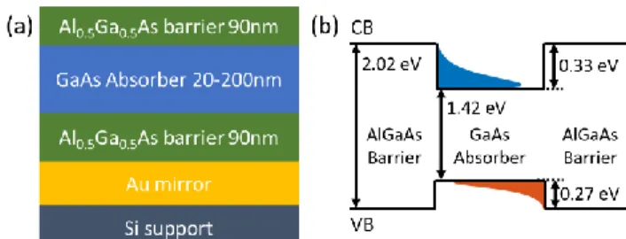
We fabricated four samples, with GaAs absorbers of thicknesses 20, 50, 100, and 200 nm (Figure 1(a)). The samples are epitaxially grown by metalorganic vapor-phase epitaxy, then bonded to a silicon wafer through gold-gold bonding. Finally, the growth substrate is removed by chemical etching. The whole fabrication process, from the epitaxial growth on GaAs to the final device, has been reported previously26. For each sample, the absorber layer
is sandwiched between 2 wider-bandgap Al0.5Ga0.5As
barriers of about 90 nm thickness (Figure 1(b)). The purpose
This is the author’s peer reviewed, accepted manuscript. However, the online version of record will be different from this version once it has been copyedited and typeset.
3 of these barriers is to confine the carriers in a well-defined volume and limit the power outflow from the absorber through thermionic emission. The exact thickness of the barriers can vary due to partial etching and oxidation during the process (we determined it previously for each sample26).
The gold layer used for the bonding also plays the role of a mirror and ensures high thermal conductivity. This design makes the sample as simple as possible to analyze with PL. Indeed, since there is no substrate and the barriers have a wide bandgap, only the absorber will emit light in the spectral region of interest (between 1.35 and 1.6 eV). Also, minimizing lattice heating leads to a more accurate measurement of the carrier temperature, since we can assume the lattice remains at room temperature even under intense illumination.
Figure 1: (a) Structure of the samples measured in this study. A GaAs absorber is sandwiched between two Al0.5Ga0.5As barriers
with a higher bandgap. The structure is bonded to a silicon substrate with a gold layer to limit lattice heating. (b) Simplified band diagram of the barrier-absorber-barrier structure, along with the bandgaps and band offsets. The electron and hole energy distributions are represented in blue and red, respectively. The vast majority of the carriers in the absorber do not have enough energy to escape to the barriers through thermionic emission.
To compare the measurements for different absorber thicknesses, we need to consider the fraction 𝑃𝑎𝑏𝑠 (in W. cm−2) of the incident laser power 𝑃
𝑖𝑛𝑐 (in W. cm−2) which is absorbed in each of them:
𝑃𝑎𝑏𝑠= 𝐴𝑙𝑎𝑠𝑒𝑟× 𝑃𝑖𝑛𝑐, (1) where 𝐴𝑙𝑎𝑠𝑒𝑟 is the absorptivity of the GaAs layer at the laser wavelength. 𝐴𝑙𝑎𝑠𝑒𝑟 was determined previously26 for each sample by fitting absorptivity measurements with a transfer matrix method27,28. We consider 𝐴
𝑙𝑎𝑠𝑒𝑟 is independent of the incident power, because the laser energies considered are far above the bandgap.
To determine the carrier temperature in the absorber as a function of the absorbed power, we measure the PL spectra at room temperature under laser illumination of increasing intensity in the four samples. We consider two
laser wavelengths of 532 and 638 nm corresponding to
photon energies of 2.33 and 1.94 eV, respectively. These energies are significantly higher than the absorber bandgap
(1.42 eV), such that we can expect a significant part of the incident power to be thermalized. The photons emitted by the 638 nm laser have less energy than the barrier bandgap
(2.02 eV). Photocarriers are thus generated only in the absorber, which is not the case for the 532 nm laser (more
detail on how this impacts the estimation of the absorbed power in Supplementary Information). Thanks to these two
different lasers, we will be able to analyze the wavelength dependence of thermalization. The series of spectra obtained for the 200 nm-thick GaAs absorber with the 532
nm laser is shown in Figure 2.
Figure 2: PL spectral photon flux (in arbitrary units) as a function of the photon energy, acquired at different absorbed powers for the 200 nm-thick GaAs absorber sample with a 532 nm
illumination. The laser spot size is about 19 µm in radius (see Supplementary Information).
The PL spectral photon flux (in s−1. m−2. eV−1) of a semiconductor with a Lambertian emission profile follows the generalized Planck law29
𝜙(𝐸) = 𝐴(𝐸)2𝐸 2 ℎ3𝑐2[exp ( 𝐸 − 𝜇 𝑘𝐵𝑇 ) − 1] −1 , (2) where 𝐸 is the photon energy, 𝐴(𝐸) is the absorptivity of the GaAs layer (considered independent of the emission angle), ℎ is the Planck constant, 𝑐 is the speed of light, 𝑘𝐵 is the Boltzmann constant, 𝜇 is the chemical potential of the radiation and 𝑇 is the temperature of the radiation. In the Boltzmann approximation, Eq. (1) becomes
𝜙(𝐸) ≈ 𝐾𝐴(𝐸)𝐸2exp (− 𝐸 𝑘𝐵𝑇
) , (3)
where 𝐾 is a parameter independent of the photon energy (it depends on the absorber thickness and illumination conditions but has no impact on the carrier temperature determination). If electrons and holes are at the same
This is the author’s peer reviewed, accepted manuscript. However, the online version of record will be different from this version once it has been copyedited and typeset.
4 temperature, then 𝑇 is also the temperature of the carriers. If electrons and holes are at different temperatures, Eq. (2) is still valid, with 𝑇 related to the temperature of the carrier populations30,31. We will consider here, as is usually assumed,
that the carrier temperatures are the same. The same analysis could be conducted for different electron and hole temperatures.
A simple way to extract the carrier temperature 𝑇 from PL measurements is the slope method20. This method
assumes the absorptivity is independent of 𝐸 on a certain range above the bandgap to extract the temperature directly from the slope of the PL spectrum in logarithmic scale in that range. However, in the ultrathin systems considered here, Fabry-Perot resonances appear between the front interface and the back mirror26. These resonances
result in strong absorption variations that can lead to significant errors in the carrier temperature assessment.
We have proposed an alternative method to extract the temperature in thin heterostructures32, where we consider
the ratio between the PL spectra obtained at two different laser fluences labeled 1 and 𝑛. Assuming the absorptivity at a given energy is independent of the absorbed power, we have ln (𝜙𝑛(𝐸) 𝜙1(𝐸)) = ( 1 𝑘𝐵𝑇1− 1 𝑘𝐵𝑇𝑛) 𝐸 + cste. (4) The high-energy slope of this ratio gives directly the temperature of the carriers. This approach is as simple to implement as the slope method, but presents the extra advantage of removing the influence of the absorption variations with 𝐸 . Also, both these methods are much simpler to apply than a full fitting4 of Eq. (2) since there is
no need for an absolute calibration of the photoluminescence intensity, and there is only one parameter to fit.
The PL ratios are shown in Figure 3(a), for the PL spectra of the 200 nm-thick GaAs absorber presented in Figure 2. The temperature determination is about twice more accurate with the ratio method than with the slope method for the 200 nm absorber case (Figure 3(b)).
This method can be used as long as 𝐴(𝐸) is independent of the absorbed power. Close to the bandgap, intensity-dependent band filling occurs, which means the temperature needs to be determined sufficiently far above the bandgap (in our case, above 1.53 eV).
Figure 3: (a) PL ratios 𝜙𝑛/𝜙1 in log scale as a function of the photon energies, for the PL data of the 200 nm-thick GaAs absorber with
the 532 nm source, shown in Figure 2. The high-energy slope of these curves can be fitted following Eq. (4), from which we can extract the temperature for all absorbed powers. (b) Carrier temperature increase as a function of absorbed power, for the ratio method (in blue) and the slope method (in red), with error bars. The error on the temperature determination is about twice lower when considering the ratio method. (The points for the slope method are slightly shifted horizontally to make the comparison easier).
3. RESULTS
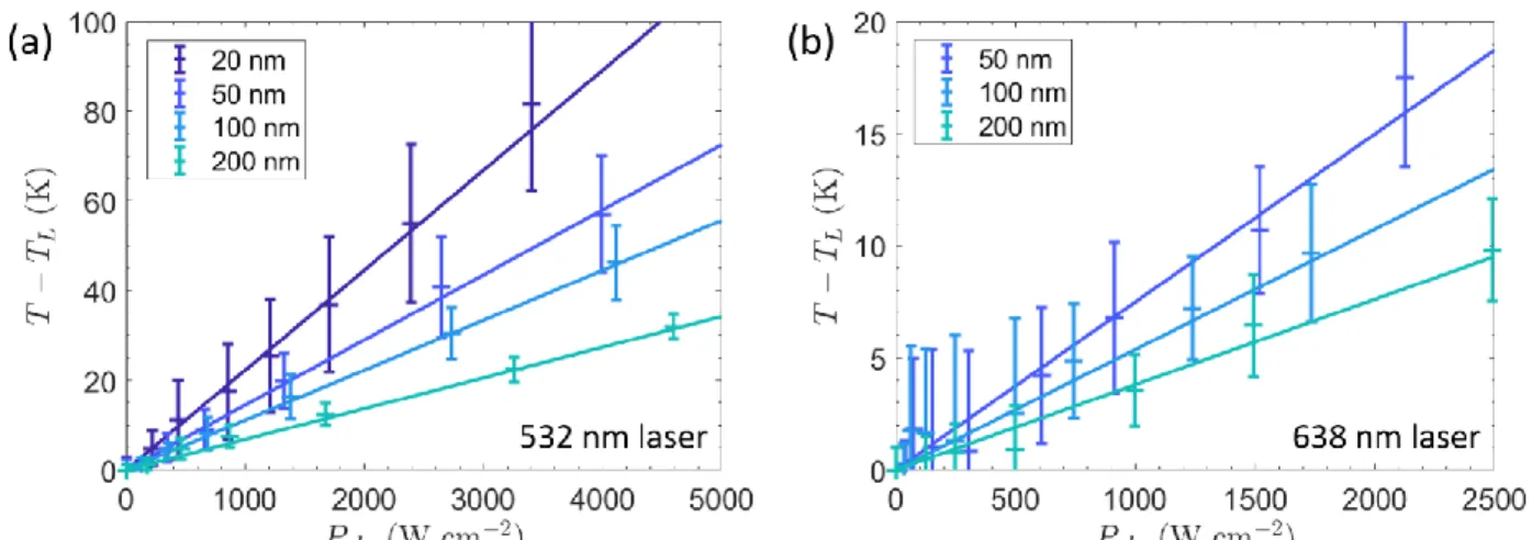
Using the PL ratio method, we determine the carrier temperature increase as a function of the absorbed power for all samples, and both lasers (see Supplementary
Information for the uncertainty calculation for the temperature and the absorbed power). We show the results for both lasers in Figure 4 (except for the 20 nm absorber with the 638 nm laser, not shown due to large uncertainties).
This is the author’s peer reviewed, accepted manuscript. However, the online version of record will be different from this version once it has been copyedited and typeset.
5
Figure 4: Carrier temperature increase 𝑇 − 𝑇𝐿 determined from the ratio method as a function of the absorbed power 𝑃𝑎𝑏𝑠, for the
different GaAs absorbers thicknesses (a) for a 532 nm laser illumination. (b) for a 638 nm laser illumination. For all wavelengths and thicknesses, we observe a proportionality between both quantities.
The first thing to be noted is that the temperature increase is relatively modest, always below 100 K in all samples, within the power range considered. Therefore, we are at the onset of the generation of hot carriers. Because the power range is higher with our 532 nm laser, the temperature increase with the 638 nm laser is even more limited, down to about 20 K. Still, because the error is small, we can confirm that for each sample and laser wavelength, we observe hot carriers. To the best of our knowledge, this is the first time that hot carriers have been measured after transferring the epitaxial layer onto a host substrate, an important step for the effective utilization of hot carriers in devices.
A remarkable feature of all the measurements in Figure 4 is that the inferred carrier temperature increases proportionally with the absorbed power 𝑃𝑎𝑏𝑠. We can translate this observation into a linear relationship
𝑃𝑎𝑏𝑠= 𝑄𝑎𝑏𝑠(𝑇 − 𝑇𝐿), (5) where 𝑇 is the carrier temperature, 𝑇𝐿 is the lattice temperature, and 𝑄𝑎𝑏𝑠 (in W. cm−2. K−1 ) is the proportionality coefficient between power and temperature increase. The factor 𝑄𝑎𝑏𝑠 is analogous to the thermalization coefficient 𝑄 defined by Le Bris et al.33, who first observed
similar linearity. In the discussion, we will justify why we modified the relationship between thermalized power and carrier temperature increase compared to that reference. To get a better hot-carrier absorber, 𝑄𝑎𝑏𝑠 should be as small as possible so that we can generate hot carriers with
relatively low incident power. We extract a coefficient 𝑄𝑎𝑏𝑠 for every sample and laser wavelength (Figure 5).
This coefficient depends on the absorber thickness and decreases with the absorber thickness: for the same absorbed power, the carrier temperature is higher in thinner absorbers (Figure 5). This result agrees with the general argument made by Le Bris et al. that the thermalization rate should decrease in thinner absorbers23.
Another key observation is that 𝑄𝑎𝑏𝑠 depends on the laser wavelength: it is higher for longer wavelengths. Part of the reason for this will be explained in the discussion, section 4.1, which will lead to an improved definition of the thermalization coefficient 𝑄.
Figure 5: Proportionality coefficient 𝑄𝑎𝑏𝑠 as a function of the
absorber thickness for both laser wavelengths. 𝑄𝑎𝑏𝑠 increases as
the absorber thickness increases and is higher for a longer laser
This is the author’s peer reviewed, accepted manuscript. However, the online version of record will be different from this version once it has been copyedited and typeset.
6 wavelength. The data for both lasers are slightly shifted along the horizontal axis to improve visibility.
4. DISCUSSION
4.1. Relation between absorbed and thermalized power
In the previous section, we observed a linear evolution of the carrier temperature increase with the absorbed power 𝑃𝑎𝑏𝑠 . To analyze the relationship between thermalized power 𝑃𝑡ℎ and carrier temperature, we first need to express 𝑃𝑡ℎ as a function of 𝑃𝑎𝑏𝑠. Le Bris et al. previously assumed33, for simplicity, that all the absorbed
power should be thermalized (𝑃𝑡ℎ≈ 𝑃𝑎𝑏𝑠). but we would like to revisit this hypothesis.
The thermalized power is the amount of power dissipated by photo-generated electrons and holes before they recombine. “Because interband recombination rates (both radiative and non-radiative) tend to be much slower (typically in nanoseconds) than electron-phonon scattering rates (typically in picoseconds), the processes of thermalization and recombination can be considered independently.” The absorbed power is dissipated entirely through a combination of interband recombinations 𝑃𝑖𝑛𝑡𝑒𝑟 and thermalized power 𝑃𝑡ℎ, leading to the detailed balance equation
𝑃𝑎𝑏𝑠= 𝑃𝑖𝑛𝑡𝑒𝑟+ 𝑃𝑡ℎ. (6) Under a laser illumination, all electron-hole pairs are generated with the same energy 𝐸𝑙𝑎𝑠𝑒𝑟. Let us call the average energy dissipated through interband recombinations 〈𝐸𝑖𝑛𝑡𝑒𝑟〉. 𝑃𝑡ℎ can be expressed as a function of the absorbed power:
𝑃𝑡ℎ=𝐸𝑙𝑎𝑠𝑒𝑟− 〈𝐸𝑖𝑛𝑡𝑒𝑟〉
𝐸𝑙𝑎𝑠𝑒𝑟 𝑃𝑎𝑏𝑠. (7)
This model assumes that the Auger effect and impact ionization are negligible and that the mechanisms related to interband recombinations are independent of those of thermalization. These interband recombinations can be divided between radiative and non-radiative recombinations.
On one hand, because hot electrons and holes each have an average kinetic energy of 3
2𝑘𝐵𝑇 (3D system), the average energy of non-radiative recombinations should be
〈𝐸𝑖𝑛𝑡𝑒𝑟〉𝑛𝑟𝑎𝑑≈ 𝐸𝐺+ 3𝑘𝐵𝑇, (8)
where 𝐸𝐺= 1.424 eV is the bandgap of GaAs at room temperature.
On the other hand, the average energy of radiatively recombined photons, assuming step absorption and in the Boltzmann approximation, is
〈𝐸𝑖𝑛𝑡𝑒𝑟〉𝑟𝑎𝑑≈ 𝐸𝐺+ 𝑘𝐵𝑇. (9) This value is different from Eq. (8) because of momentum conservation (not every electron can recombine radiatively with every hole). Here, we will assume that non-radiative recombinations dominate, as is typically the case, and thus consider Eq. (8) . Moreover, carrier heating is relatively low in our experiments. Therefore, we can consider 𝑇 ≈ 𝑇𝐿 in Eq. (8) to obtain a proportionality between 𝑃𝑡ℎ and 𝑃𝑎𝑏𝑠 , independent (to a first-order approximation in 𝑇 − 𝑇𝐿) of the carrier temperature:
𝑃𝑡ℎ≈𝐸𝑙𝑎𝑠𝑒𝑟− (𝐸𝐺+ 3𝑘𝐵𝑇𝐿)
𝐸𝑙𝑎𝑠𝑒𝑟 𝑃𝑎𝑏𝑠. (10)
From Eqs. (5) and (10) , we define a thermalization coefficient 𝑄 =𝐸𝑙𝑎𝑠𝑒𝑟− (𝐸𝐺+ 3𝑘𝐵𝑇𝐿) 𝐸𝑙𝑎𝑠𝑒𝑟 𝑄𝑎𝑏𝑠, (11) such that 𝑃𝑡ℎ= 𝑄(𝑇 − 𝑇𝐿). (12) 𝑄 is independent of the carrier temperature, at least for a small temperature increase. The thermalization coefficients obtained for both lasers are shown in Figure 6. The ratio between the values obtained for both lasers is
𝑄(638)
𝑄(532)= 1.23 ± 0.52. (13)
This is the author’s peer reviewed, accepted manuscript. However, the online version of record will be different from this version once it has been copyedited and typeset.
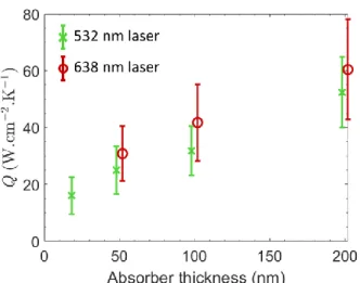
7 Figure 6: Thermalization coefficient 𝑄 as a function of the
absorber thickness for both laser wavelengths. 𝑄 increases as the absorber thickness increases and is slightly higher for a longer laser wavelength (within error bars). The data for both lasers are slightly shifted along the horizontal axis to improve visibility.
The thermalization coefficients are similar, slightly higher for the lower laser energy (with a large error bar). We will suggest a possible reason for this in the following sections.
4.2. Thermalization coefficient as a function of absorber thickness
In the previous section, we gave a broad definition of thermalization (all the power dissipation which is not related to interband recombinations). Now, we want to identify the possible mechanisms for thermalization, i.e. how the extra energy initially given to the carriers is dissipated. In GaAs, as mentioned in the introduction, the carriers interact mostly with the LO phonons, in an elastic manner, such that an equilibrium can be considered between the two populations. Therefore, thermalization corresponds to either high-energy electrons or LO phonons being dissipated from where they are generated, which can take 3 different forms (Figure 7). The first is the decay of optical phonons within the volume where carriers are generated, corresponding to a power dissipated per unit of volume 𝑝𝑡ℎ,𝑉. The second is the escape of either high-energy carriers or LO phonon through the interface, or their decay at the interface, corresponding to a power dissipated per unit of surface 𝑃𝑡ℎ,𝑆. The last is the escape of either
electrons or LO phonons laterally outside of the incident spot, where they then decay, corresponding to a power dissipated 𝑃𝑡ℎ,𝑙𝑎𝑡. The LO phonons being generated close to the center of the Brillouin zone (because the photocarriers are located there), their wave vector is very short, and their lateral diffusion is negligible relative to the spot size. Moreover, the area from which we measure a PL signal is roughly the same as the laser spot size (see Supplementary Information), indicating no significant lateral carrier diffusion. Therefore, we will assume that lateral thermalization can be neglected.
Figure 7: The power which is thermalized in the absorber can follow three paths. The first is thermalization within the volume of the absorber 𝑝𝑡ℎ,𝑉, which in GaAs is understood to originate
mostly from LO phonon decay. The second is thermalization through (or at) the interfaces 𝑃𝑡ℎ,𝑆, which is for example the case
of thermionic emission. The last is the lateral diffusion of either electrons or LO phonons 𝑃𝑡ℎ,𝑙𝑎𝑡 away from the laser spot, which
we consider negligible.
We now look at how the thermalization coefficient varies with the absorber thickness (Figure 8). We observe for both laser wavelengths an affine relationship between thermalization coefficient and thickness, which does not go through the origin. We interpret this by writing
𝑄 = 𝑑𝑞𝑉+ 2𝑄𝑆, (14) where 𝑞𝑉 (in W. cm−2. K−1. nm−1 ) is the volume thermalization coefficient and 𝑄𝑆 (in W. cm−2. K−1) is the surface thermalization coefficient of the sample series.
This is the author’s peer reviewed, accepted manuscript. However, the online version of record will be different from this version once it has been copyedited and typeset.
8
Figure 8: Thermalization coefficient 𝑄 as a function of the absorber thickness. (a) For the 532 nm laser measurement. (b) For the 638 nm laser measurement. In both cases, we observe an affine relation between both quantities, which allows us to define surface and volume contributions to thermalization following Eq. (14).
Eq. (14) confirms the idea that there are two components to thermalization (Figure 7), such that
𝑃𝑡ℎ= 𝑝𝑡ℎ,𝑉× 𝑑 + 2𝑃𝑡ℎ,𝑆. (15) The first is proportional to the absorber thickness, related to a thermalization process occurring within the absorber volume, while the second is independent of the thickness and attributable to a thermalization process occurring through the interfaces between the absorber and the barriers. The factor 2 in Eq. (14) is introduced so that 𝑄𝑆 corresponds to the thermalization through one GaAs-AlGaAs interface, both being assumed identical. Eq. (14) furthermore indicates that both the volume and surface thermalization mechanisms are proportional to the carrier temperature increase, at least up to 𝑇 − 𝑇𝐿= 100 K . Experimental values for these thermalization coefficients for both laser wavelengths are reported in Table I.
532 nm laser 638 nm laser
𝒒𝑽 (W. cm−2. K−1. nm−1) 0.20 ± 0.07 0.20 ± 0.13
𝑸𝑺 (W. cm−2. K−1) 6.4 ± 3.2 10.8 ± 6.9
Table I: Volume and surface thermalization coefficients obtained from analyzing the variations of the thermalization coefficient with the absorber thickness (Eq. (14)) in the GaAs sample series, for both laser wavelengths.
Very interestingly, we obtained the same volume thermalization coefficient for both lasers. Regarding the surface thermalization coefficient, it appears to be slightly higher with the 638 nm laser, although the uncertainty is large. The higher thermalization coefficient observed for the
638 nm laser (Figure 6) thus seems to originate purely from a larger thermalization at the interfaces.
For this sample series, the contribution of 𝑞𝑉 and 𝑄𝑆 is comparable for absorber thicknesses between 30 and 50 nm. Thicker absorbers are dominated by volume thermalization, while thinner ones mostly dissipate the power through surface thermalization. Ultrathin absorbers may therefore show high thermalization rates if the surface contribution is large.
We gave some examples of volume and surface thermalization mechanisms in the introduction. Thermalization through LO phonon decay should be the dominating thermalization mechanism within the absorber volume. Thermionic emission is a typical case of surface thermalization, where the high energy electrons escape through the barriers, decreasing the average energy of the carrier in the absorber. LO phonon transmission through the interface is another possible source of surface thermalization. In the rest of the discussion, we will look at several of these mechanisms, to see if they can explain the linear relation between thermalized power and temperature increase and if the experimental values are compatible with theoretical models.
4.3. Origin of volume thermalization
In this section, we show that the volume thermalization component is consistent with LO phonon decay. We assume that electrons interact only with the LO phonons, as is commonly considered in GaAs34. The thermalized power
density 𝑝𝑡ℎ (in W. cm−3) is the integral over the wave vectors 𝒒 of the LO phonon population that decays into acoustic phonons per unit of time, times the LO phonon energy:
This is the author’s peer reviewed, accepted manuscript. However, the online version of record will be different from this version once it has been copyedited and typeset.
9 𝑝𝑡ℎ,𝑉= 𝑛0 2 × 1 𝑉𝐵∭ d 3𝒒𝜕𝑓 𝜕𝑡(𝒒)𝐸𝐿𝑂(𝒒) , (16) where 𝑛0 is the density of atoms in GaAs (in cm−3), 𝑉𝐵 is the volume of the first Brillouin zone, 𝑓 is the occupation number at wave vector 𝒒, and 𝐸𝐿𝑂 is the energy of the wave vector. The factor 1/2 arises because there is 1 LO phonon branch in the first Brillouin zone of a fcc lattice for 2 atoms in the real-space Wigner-Seitz cell35. The integral runs over
the first Brillouin zone, such that ∭ 𝑑3𝒒 = 𝑉
𝐵. For a fcc lattice, the volume of the Brillouin zone is
𝑉𝐵= 4 × (2𝜋 𝑎)
3
, (17)
where 𝑎 is the lattice parameter of GaAs. We define the wave vector module |𝒒𝑩| =
2𝜋
𝑎 such that 𝑉𝐵= 4 × |𝒒𝑩| 3. In the relaxation time approximation, we can write34
𝜕𝑓 𝜕𝑡(𝒒) =
𝑓(𝒒) − 𝑓𝑒𝑞(𝒒)
𝜏(𝒒) , (18)
where 𝜏 is the lifetime of the phonons, 𝑓 is the non-equilibrium phonon density and 𝑓𝑒𝑞 is the Bose-Einstein LO phonon distribution at lattice temperature, independent of the wave vector:
𝑓𝑒𝑞 = 𝑓𝐵𝐸(𝑇𝐿) =
1 exp (𝐸𝐿𝑂
𝑘𝐵𝑇𝐿) − 1
. (19)
Because only the phonons with a low wave vector can couple with the electrons, we consider the Einstein model where the phonon energy is independent of its wave vector. For simplicity, we also assume that all phonons have the same lifetime36 𝜏(𝒒) = 𝜏 𝐿𝑂, such that 𝑝𝑡ℎ,𝑉 =𝑛0 2 𝐸𝐿𝑂 𝜏𝐿𝑂× 1 𝑉𝐵∭ d 3𝒒[𝑓(𝒒) − 𝑓 𝑒𝑞] . (20) Not all LO phonons couple with photocarriers. LO phonons with a large wave vector cannot be generated during hot-carrier thermalization and thus remain at equilibrium. We consider as an approximation that only the LO phonons with a wave vector with a module lower than a certain value |𝒒𝒎𝒂𝒙| are coupled with the electrons. We also assume that these phonons are at the same temperature as the electrons. There is also a minimum wave vector |𝒒𝒎𝒊𝒏| such that phonons with a small wave vector are also not
coupled with the electrons, but it can be neglected because |𝒒𝒎𝒊𝒏|3≪ |𝒒𝒎𝒂𝒙|3. The phonon number then follows one of two Bose-Einstein distributions:
𝑓(𝒒) = {𝑓𝐵𝐸(𝑇) if |𝒒| < |𝒒𝒎𝒂𝒙|
𝑓𝐵𝐸(𝑇𝐿) otherwise . (21) The thermalized power density is then obtained by developing the integral in Eq. (20) in spherical coordinates, leading to 𝑝𝑡ℎ,𝑉 = 𝜋 6 𝑛0𝐸𝐿𝑂 𝜏𝐿𝑂 [𝑓𝐵𝐸(𝑇) − 𝑓𝐵𝐸(𝑇𝐿)] ( |𝒒𝒎𝒂𝒙| |𝒒𝑩| ) 3 . (22) If the temperature of the carriers is much higher than that of the lattice, then we can neglect the second term in the brackets. In the Boltzmann approximation, we then recover the expression derived by Le Bris et al.33. For small
temperature increases like those we observe (less than 200 K for a lattice temperature 𝑇𝐿= 300 K), the variation of phonon occupancy is very well approximated by a first-order Taylor expansion around 𝑇 − 𝑇𝐿= Δ𝑇:
𝑓𝐵𝐸(𝑇) − 𝑓𝐵𝐸(𝑇𝐿) ≈ 𝛽 × Δ𝑇, (23) with 𝛽 = 𝐸𝐿𝑂 𝑘𝐵𝑇𝐿2 exp (𝐸𝐿𝑂 𝑘𝐵𝑇𝐿) [exp (𝐸𝐿𝑂 𝑘𝐵𝑇𝐿) − 1] 2. (24)
This leads to the expression
𝑝𝑡ℎ,𝑉 =𝜋 6 𝛽𝑛0𝐸𝐿𝑂 𝜏𝐿𝑂 (|𝒒𝒎𝒂𝒙| |𝒒𝑩| ) 3 Δ𝑇. (25)
Eq. (25) could explain the linear relationship we observe between thermalized power and temperature increase, provided the other quantities are independent of the temperature. We can express the volume thermalization coefficient 𝑞𝑉=𝜋 6 𝛽𝑛0𝐸𝐿𝑂 𝜏𝐿𝑂 ( |𝒒𝒎𝒂𝒙| |𝒒𝑩| ) 3 . (26)
Most of the parameters in Eq. (26) are well known in GaAs and are independent (at least to a first-order approximation) of the carrier temperature. We consider 𝑛0= 4.42 1022 cm−3, 𝐸𝐿𝑂= 36.1 10−3 eV , 𝜏𝐿𝑂= 3.5 ps
This is the author’s peer reviewed, accepted manuscript. However, the online version of record will be different from this version once it has been copyedited and typeset.
10 and |𝒒𝑩| = 1.11 108 cm−1. The proportionality factor 𝛽 = 2.0 10−3 K−1 is obtained directly from 𝐸
𝐿𝑂 and the lattice temperature 𝑇𝐿= 296 K (Eq. (24)). The main uncertainty comes from the fraction of phonon modes coupled with the electrons, related to the wave vector |𝒒𝒎𝒂𝒙| . We can estimate its value using the volume thermalization coefficient 𝑞𝑉 determined experimentally (Table I):
|𝒒𝒎𝒂𝒙| ≈ 3.3 ± 0.4 × 106 cm−1. (27) |𝒒𝒎𝒂𝒙| is relatively small compared to |𝒒𝑩| , verifying that only a small fraction of the phonon modes are coupled to the electrons. We want to check whether this order of magnitude for 𝑞𝑚𝑎𝑥 is coherent with the distribution of non-equilibrium phonon densities. We assumed that the phonon occupation number follows the Bose-Einstein distribution at the carrier temperature for the phonon modes coupled with the electrons, while it is equal to the equilibrium distribution for uncoupled modes. In reality, there is no such sharp distinction between coupled and non-coupled modes, and the distribution with |𝒒| should be smoother.
We simulate the non-equilibrium distribution of phonons following the work of Tsai34 (Figure 9). The overall
shape of the distribution does not change much as we change the carrier temperature between 300 and 400 K, so we can assume that |𝒒𝒎𝒂𝒙| is independent of the incident power to a first-order approximation. The thermalization coefficient is thus also independent of the laser wavelength, as observed experimentally. The experimental value we determined for |𝒒𝒎𝒂𝒙| agrees with the wave vector at which the modeled non-equilibrium distribution strongly decreases. This meaning LO phonon decay is likely to be responsible for volume thermalization. The precise calculation of the power thermalized in this way requires the knowledge of the chemical potential of the carriers, and will be the object of a future publication.
Figure 9: Non-equilibrium LO phonon distribution for a lattice temperature 𝑇𝐿= 300 K and a carrier temperature 𝑇 varied
between 300 and 400 K. The dashed lines are the distributions introduced in Eq. (21): the modes with a wave vector smaller that |𝒒𝒎𝒂𝒙| (determined experimentally in Eq. (27)) follow a
Bose-Einstein distribution at the temperature 𝑇. The continuous lines are the non-equilibrium distributions as calculated from Tsai34 for a Fermi level for the electrons 30 meV below the
conduction band. Only the electron contribution to
thermalization is considered. We see that the non-equilibrium distributions decrease around the experimentally-derived value of |𝒒𝒎𝒂𝒙|, independently from the carrier temperature.
4.4. Possible origins of surface thermalization
The surface thermalization coefficient corresponds to energy loss from the electron-LO phonon system, at or through the absorber interfaces. We will show here that it does not originate from the transmission of LO phonons into the barriers.
Because optical phonon dispersion curves are nearly flat close to the zone center, their group speed is small compared to that of acoustic phonons, so that their transport properties are usually neglected. However, since we are concerned only with LO phonons and because our absorbers are very thin, the contribution of LO phonon transmission to hot-carrier thermalization should be assessed. We assume that a fraction 𝜗(𝒒) of the incident LO phonons are transmitted through the interface. The power flow of LO phonons through the interface with the barrier is calculated similarly to the volume thermalization through LO phonon decay, where we now need to consider the speed of LO phonons along the direction normal to the interface 𝑣𝑧. The power which is transmitted to one of the barriers writes
𝑃𝑡ℎ,𝑆 = 𝑛0 2𝑉𝐵∭ d
3𝒒𝜗(𝒒)[𝑓(𝒒) − 𝑓
𝑒𝑞(𝒒)]𝐸𝐿𝑂(𝒒)𝑣𝑧(𝒒) , (28)
This is the author’s peer reviewed, accepted manuscript. However, the online version of record will be different from this version once it has been copyedited and typeset.
11 where the integral runs over the wave vectors in the first Brillouin zone satisfying 𝑣𝑧(𝒒) ≥ 0. Again, we assume that the phonon energy is independent of the wave vector and that phonons with a wave vector of modulus lower than |𝒒𝒎𝒂𝒙| are at temperature 𝑇, while the others remain cold. We also consider the linear expansion around Δ𝑇 such that
𝑃𝑡ℎ,𝑆= 𝛽𝑛0𝐸𝐿𝑂 2 × Δ𝑇 × 1 𝑉𝐵∭ d 3𝒒𝜗(𝒒)𝑣 𝑧(𝒒) , (29) where the integral now runs over the half-sphere of radius |𝒒𝒎𝒂𝒙| and 𝑣𝑧(𝒒) ≥ 0 . This value admits an upper limit, provided 𝜗(𝒒) = 1 for all wave vectors:
𝑃𝑡ℎ,𝑆 ≤ 𝛽𝑛0𝐸𝐿𝑂 2 × Δ𝑇 × 1 𝑉𝐵 ∭ d3𝒒 𝑣 𝑧(𝒒) . (30) The integral expression can be developed in spherical coordinates with 𝑣𝑧= 𝑣 cos 𝜑, leading to
∭ d3𝒒𝑣
𝑧(𝒒) = 𝜋 ∫ d𝑞 𝑞2 𝑣(𝑞) |𝒒𝒎𝒂𝒙|
0
. (31) The LO phonon speed is to a first approximation (|𝒒| ≪ |𝒒𝑩|) proportional to the wave vector:
𝑣(𝑞) =𝜕𝜔𝐿𝑂
𝜕𝑞 ≈ 𝛼0× 𝑞, (32) where 𝜔𝐿𝑂 is the frequency of LO phonons. We can get an analytic expression for 𝛼0 by considering the dispersion relation in the absence of polar interactions:
𝛼0= 𝐸𝐿𝑂 ℏ ( 𝑀𝐺𝑎𝑀𝐴𝑠 2(𝑀𝐺𝑎+ 𝑀𝐴𝑠)2 𝑎2) , (33) where 𝑀𝐺𝑎 and 𝑀𝐴𝑠 are the atomic masses of Ga and As, respectively, and 𝑎 is the lattice parameter of GaAs. As mentioned, this description ignores the polar nature of GaAs, which results in separate LO and TO dispersion relations with phonon energies different from the one derived in Eq. (33) . It is possible to fit 𝛼0 from experimental or numerical data, but the variety of models and the small curvature mean there is necessarily a lot of uncertainty. We will thus consider the value obtained in Eq. (33) as an order of magnitude for this calculation.
Overall, the upper limit for the power thermalized by LO phonon transport through an interface is
𝑃𝑡ℎ,𝑆≤ 𝜋 32𝛼0𝛽𝑛0𝐸𝐿𝑂|𝒒𝒎𝒂𝒙| ( |𝒒𝒎𝒂𝒙| |𝒒𝑩| ) 3 Δ𝑇. (34) As for the LO phonon decay term, the LO phonon transmission appears to be proportional to the temperature increase Δ𝑇, which stems from the linear expansion of the difference in the occupation functions. The surface thermalization coefficient thus has an upper limit
𝑄𝑆≤ 𝜋 32𝛼0𝛽𝑛0𝐸𝐿𝑂|𝒒𝒎𝒂𝒙| ( |𝒒𝒎𝒂𝒙| |𝒒𝑩| ) 3 . (35) We consider for |𝒒𝒎𝒂𝒙| the value determined from the experimental volume thermalization coefficient (Eq. (27)), leading to
𝑄𝑆≤ 9.4 × 10⁻² W. cm−2. K−1. (36) This value is more than one order of magnitude smaller than the experimental measurements. Moreover, the LO phonon energies of GaAs and Al0.5Ga0.5As differ
significantly37, such that the transmission coefficient 𝜗 is
expected to be much lower than 1. Therefore, it seems like the contribution of LO phonon transmission to thermalization can be considered negligible here. This important result means that as long as the experimentally measured surface thermalization remains significantly higher than in Eq. (36) , there is no need to engineer a phonon mismatch between the absorber and barrier materials.
The principal remaining candidate for surface thermalization is the thermionic emission of electrons over the barriers7,14,38. Thermionic emission agrees qualitatively
with the observation that the surface thermalization coefficient is higher for the longer laser wavelengths. Indeed, a longer wavelength will lead to more photocarriers generated for the same absorbed power, which should lead to a higher chemical potential in the absorber. Moreover, the 638 nm laser, contrarily to the 532 nm laser, does not have enough energy to excite carriers in the barriers, such that the chemical potential in the barriers should be lower for the longer wavelength. Therefore, the thermionic power flux from the absorber to the barriers should be higher with the longer laser wavelength. As a consequence, the thermalization coefficient should increase with the laser wavelength, which is what we observe experimentally. An in-depth analysis of the PL spectra to determine the chemical potentials is required to determine whether thermionic emission is indeed the principal reason for surface thermalization.
This is the author’s peer reviewed, accepted manuscript. However, the online version of record will be different from this version once it has been copyedited and typeset.
12 Other possible origins for the thermalization coefficient involve LO phonon or electron scattering events at the interface. These terms are especially difficult to estimate, as they depend on defect states between the absorber and the barrier. What we can say at this stage is that there is significant thermalization through the interfaces in this sample series, especially for ultra-thin absorbers where it dominates the LO phonon decay volume process.
5. CONCLUSIONS
We reported power-dependent PL characterization of ultrathin heterostructures with two different laser wavelengths at room temperature. The samples considered are GaAs absorbers of four different thicknesses between 20 and 200 nm sandwiched between AlGaAs barriers, transferred onto a host substrate. The simplicity of this series provides a way to shed light on hot-carrier thermalization mechanisms and constitutes a step towards the fabrication of more complex hot-carrier solar cell designs.
We considered a PL ratio method to extract the carrier temperature in these ultrathin layers with relatively low uncertainty. We observed a linear relationship between the absorbed power and the temperature increase of the carriers in all samples, enabling the extraction of a proportionality coefficient 𝑄𝑎𝑏𝑠. By relating absorbed and thermalized power, we determined a thermalization coefficient 𝑄 for all absorber thicknesses and laser wavelengths.
We obtained an affine relationship between the thermalization coefficient and the absorber thickness. From this relationship, we identified two distinct thermalization mechanisms. The first mechanism is a volume effect proportional to the absorber thickness, attributed to LO phonon decay. The second mechanism is a surface contribution independent of the absorber thickness, which highlights the importance of the interfaces in the hot-carrier thermalization. Although its exact origin remains unclear, we confirmed that LO phonon transmission through the barriers is negligible so that there is no need to consider the barriers’ LO phonon energy as a design criterion.
Overall, the definition we provided for the thermalization coefficient will be helpful to compare the quality of hot-carrier absorbers across different materials and experimental setups. Furthermore, our approach can be applied to identify surface and volume thermalization contributions in any material. This work also emphasizes the crucial importance of developing ultrathin absorbers as well as the need to consider their interfaces carefully. These ultrathin absorbers could eventually enable high-efficiency
hot-carrier solar cells, provided high absorption can be maintained. This absorption enhancement requires the implementation of advanced light trapping schemes, for which promising experimental results were achieved in 25 and 200 nm-thick GaAs layers39,40.
Future work includes a more advanced fit of the PL data to extract the chemical potential in the absorber and determine more accurately the contributions of LO phonon decay and thermionic emission. It will also be of interest to investigate quantum confinement of carriers in ultrathin absorbers and its impact on thermalization.
SUPPLEMENTARY MATERIAL
See supplementary material for a detailed analysis of the error on the determination of the carrier temperature and the thermalization coefficient.
ACKNOWLEDGMENTS
This work was performed within the framework of LIA NextPV currently IRP NextPV-II, with support from CNRS (INC and INSIS) and RCAST/University of Tokyo. Authors would like to acknowledge the support of the Japanese MEXT scholarship program, the Japan Society for the Promotion of Science (JSPS) KAKENHI Grant Number 19H02541, the French ANR project ICEMAN Grant Number ANR-19-CE05-0019, the IPVF PROOF program, and the Energy4Climate Interdisciplinary Center (E4C) of IP Paris and Ecole des Ponts ParisTech (France).
AIP PUBLISHING DATA SHARING POLICY
The data that support the findings of this study are available from the corresponding author upon reasonable request.
REFERENCES
[1] Shockley, W. and Queisser, H. J., “Detailed Balance Limit of Efficiency of p‐n Junction Solar Cells,” Journal of Applied Physics 32(3), 510–519 (1961).
[2] Ross, R. T. and Nozik, A. J., “Efficiency of hot‐carrier solar energy converters,” Journal of Applied Physics 53(5), 3813–3818 (1982).
[3] Dimmock, J. A. R., Day, S., Kauer, M., Smith, K. and Heffernan, J., “Demonstration of a hot-carrier photovoltaic cell,” Prog. Photovolt: Res. Appl. 22(2), 151– 160 (2014).
[4] Nguyen, D.-T., Lombez, L., Gibelli, F., Boyer-Richard, S., Le Corre, A., Durand, O. and Guillemoles, J.-F., “Quantitative
This is the author’s peer reviewed, accepted manuscript. However, the online version of record will be different from this version once it has been copyedited and typeset.
13 experimental assessment of hot carrier-enhanced solar cells at room temperature,” Nature Energy 3(3), 236–242 (2018).
[5] Hirst, L. C., Walters, R. J., Führer, M. F. and Ekins-Daukes, N. J., “Experimental demonstration of hot-carrier photo-current in an InGaAs quantum well solar cell,” Appl. Phys. Lett. 104(23), 231115 (2014).
[6] Jehl, Z., Suchet, D., Miyashita, N., Behagel, B., Giteau, M., Delamarre, A., Jeco, B. M. F. Y., Guillemoles, J. and Okada, Y., “Hot Carrier Extraction Using Energy Selective Contacts and Feedback On The Remaining Distribution,” 2018 IEEE 7th World Conference on Photovoltaic Energy Conversion (WCPEC) (A Joint Conference of 45th IEEE PVSC, 28th PVSEC 34th EU PVSEC), 1814–1816 (2018).
[7] Suchet, D., Jehl, Z., Okada, Y. and Guillemoles, J.-F., “Influence of Hot-Carrier Extraction from a Photovoltaic Absorber: An Evaporative Approach,” Phys. Rev. Applied 8(3), 034030 (2017).
[8] Conibeer, G. J., Jiang, C.-W., König, D., Shrestha, S., Walsh, T. and Green, M. A., “Selective energy contacts for hot carrier solar cells,” Thin Solid Films 516(20), 6968–6973 (2008).
[9] Le bris, A., “Etude de faisabilité d’un dispositif photovoltaïque à porteurs chauds,” Ph.D. thesis (2011). [10] Fröhlich, H., “Electrons in lattice fields,” Advances in
Physics 3(11), 325–361 (1954).
[11] Klemens, P. G., “Anharmonic Decay of Optical Phonons,” Phys. Rev. 148(2), 845–848 (1966).
[12] Shah, J., Pinczuk, A., Gossard, A. C. and Wiegmann, W., “Energy-Loss Rates for Hot Electrons and Holes in GaAs Quantum Wells,” Phys. Rev. Lett. 54(18), 2045–2048 (1985).
[13] Hathwar, R., Zou, Y., Jirauschek, C. and Goodnick, S. M., “Nonequilibrium electron and phonon dynamics in advanced concept solar cells,” J. Phys. D: Appl. Phys. 52(9), 093001 (2019).
[14] Shakouri, A., LaBounty, C., Piprek, J., Abraham, P. and Bowers, J. E., “Thermionic emission cooling in single barrier heterostructures,” Appl. Phys. Lett. 74(1), 88–89 (1998).
[15] Yangui, A., Bescond, M., Yan, T., Nagai, N. and Hirakawa, K., “Evaporative electron cooling in asymmetric double barrier semiconductor heterostructures,” 1, Nature Communications 10(1), 4504 (2019).
[16] Behaghel, B., Tamaki, R., Chen, H.-L., Rale, P., Lombez, L., Shoji, Y., Delamarre, A., Cattoni, A., Collin, S., Okada, Y. and Guillemoles, J.-F., “A hot-carrier assisted InAs/AlGaAs quantum-dot intermediate-band solar cell,” Semicond. Sci. Technol. 34(8), 084001 (2019).
[17] Conibeer, G., Shrestha, S., Huang, S., Patterson, R., Xia, H., Feng, Y., Zhang, P., Gupta, N., Tayebjee, M., Smyth, S., Liao, Y., Lin, S., Wang, P., Dai, X. and Chung, S., “Hot carrier solar cell absorber prerequisites and candidate material systems,” Solar Energy Materials and Solar Cells 135, 124– 129 (2015).
[18] Pelouch, W. S., Ellingson, R. J., Powers, P. E., Tang, C. L., Szmyd, D. M. and Nozik, A. J., “Comparison of hot-carrier relaxation in quantum wells and bulk GaAs at high carrier densities,” Phys. Rev. B 45(3), 1450–1453 (1992). [19] Rosenwaks, Y., Hanna, M. C., Levi, D. H., Szmyd, D. M.,
Ahrenkiel, R. K. and Nozik, A. J., “Hot-carrier cooling in GaAs: Quantum wells versus bulk,” Phys. Rev. B 48(19), 14675–14678 (1993).
[20] Hirst, L. C., Yakes, M. K., Bailey, C. G., Tischler, J. G., Lumb, M. P., González, M., Führer, M. F., Ekins-Daukes, N. J. and Walters, R. J., “Enhanced Hot-Carrier Effects in InAlAs/InGaAs Quantum Wells,” IEEE Journal of Photovoltaics 4(6), 1526–1531 (2014).
[21] Conibeer, G., Zhang, Y., Bremner, S. P. and Shrestha, S., “Towards an understanding of hot carrier cooling mechanisms in multiple quantum wells,” Jpn. J. Appl. Phys. 56(9), 091201 (2017).
[22] Zhang, Y., Tang, L., Zhang, B., Wang, P. and Xu, C., “Quantitative study on the mechanisms underlying the phonon bottleneck effect in InN/InGaN multiple quantum wells,” Appl. Phys. Lett. 116(10), 103104 (2020).
[23] Bris, A. L., Rodiere, J., Colin, C., Collin, S., Pelouard, J. L., Esteban, R., Laroche, M., Greffet, J. J. and Guillemoles, J. F., “Hot Carrier Solar Cells: Controlling Thermalization in Ultrathin Devices,” IEEE Journal of Photovoltaics 2(4), 506–511 (2012).
[24] Achermann, M., Bartko, A. P., Hollingsworth, J. A. and Klimov, V. I., “The effect of Auger heating on intraband carrier relaxation in semiconductor quantum rods,” 8, Nature Phys 2(8), 557–561 (2006).
[25] Strauss, U., Rühle, W. W. and Köhler, K., “Auger recombination in intrinsic GaAs,” Appl. Phys. Lett. 62(1), 55–57 (1993).
[26] Giteau, M., Watanabe, K., Miyashita, N., Sodabanlu, H., Atlan, F., Suchet, D., Collin, S., Guillemoles, J.-F. and Okada, Y., “Fabrication and optical characterization of ultrathin III-V transferred heterostructures for hot-carrier absorbers,” Physics, Simulation, and Photonic Engineering of Photovoltaic Devices IX 11275, 1127507, International Society for Optics and Photonics (2020).
[27] Knittl, Z., [Optics of thin films: an optical multilayer theory], Wiley, London, New York (1976).
[28] Acquaroli, L. N., “Matrix method for thin film optics,” arXiv:1809.07708 [physics] (2018).
[29] Wurfel, P., “The chemical potential of radiation,” J. Phys. C: Solid State Phys. 15(18), 3967 (1982).
[30] Gibelli, F., Lombez, L. and Guillemoles, J.-F., “Two carrier temperatures non-equilibrium generalized Planck law for semiconductors,” Physica B: Condensed Matter 498, 7–14 (2016).
[31] Whiteside, V. R., Magill, B. A., Lumb, M. P., Esmaielpour, H., Meeker, M. A., Mudiyanselage, R. R. H. H., Messager, A., Vijeyaragunathan, S., Mishima, T. D., Santos, M. B., Vurgaftman, I., Khodaparast, G. A. and Sellers, I. R., “Valence band states in an InAs/AlAsSb multi-quantum
This is the author’s peer reviewed, accepted manuscript. However, the online version of record will be different from this version once it has been copyedited and typeset.
14 well hot carrier absorber,” Semicond. Sci. Technol. 34(2), 025005 (2019).
[32] Esmaielpour, H., Suchet, D., Lombez, L., Giteau, M., Delamarre, A., Ory, D., Cattoni, A., Collin, S. and Guillemoles, J.-F., “Investigation of hot carrier spatial distributions in quantum well structures via hyperspectral luminescence imaging,” J. Appl. Phys. (in press).
[33] Bris, A. L., Lombez, L., Laribi, S., Boissier, G., Christol, P. and Guillemoles, J.-F., “Thermalisation rate study of GaSb-based heterostructures by continuous wave photoluminescence and their potential as hot carrier solar cell absorbers,” Energy & Environmental Science 5(3), 6225–6232 (2012).
[34] Tsai, C.-Y., “Theoretical model and simulation of carrier heating with effects of nonequilibrium hot phonons in semiconductor photovoltaic devices,” Progress in Photovoltaics: Research and Applications 26(10), 808–824 (2018).
[35] Kittel, C., [Introduction to Solid State Physics, 8 edition], Wiley, Hoboken, NJ (2004).
[36] Bhatt, A. R., Kim, K. W. and Stroscio, M. A., “Theoretical calculation of longitudinal‐optical‐phonon lifetime in GaAs,” Journal of Applied Physics 76(6), 3905–3907 (1994). [37] Adachi, S., [Properties of aluminium gallium arsenide], IEE,
INSPEC, London (1993).
[38] Könemann, F., Chen, I.-J., Lehmann, S., Thelander, C. and Gotsmann, B., “Imaging the Thermalization of Hot Carriers After Thermionic Emission Over a Polytype Barrier,” Phys. Rev. Applied 13(5), 054035 (2020).
[39] Massiot, I., Vandamme, N., Bardou, N., Dupuis, C., Lemaître, A., Guillemoles, J.-F. and Collin, S., “Metal Nanogrid for Broadband Multiresonant Light-Harvesting in Ultrathin GaAs Layers,” ACS Photonics 1(9), 878–884 (2014).
[40] Chen, H.-L., Cattoni, A., Lépinau, R. D., Walker, A. W., Höhn, O., Lackner, D., Siefer, G., Faustini, M., Vandamme, N., Goffard, J., Behaghel, B., Dupuis, C., Bardou, N., Dimroth, F. and Collin, S., “A 19.9%-efficient ultrathin solar cell based on a 205-nm-thick GaAs absorber and a silver nanostructured back mirror,” Nat Energy, 1–7 (2019).
This is the author’s peer reviewed, accepted manuscript. However, the online version of record will be different from this version once it has been copyedited and typeset.
This is the author’s peer reviewed, accepted manuscript. However, the online version of record will be different from this version once it has been copyedited and typeset.
This is the author’s peer reviewed, accepted manuscript. However, the online version of record will be different from this version once it has been copyedited and typeset.
This is the author’s peer reviewed, accepted manuscript. However, the online version of record will be different from this version once it has been copyedited and typeset.
This is the author’s peer reviewed, accepted manuscript. However, the online version of record will be different from this version once it has been copyedited and typeset.
This is the author’s peer reviewed, accepted manuscript. However, the online version of record will be different from this version once it has been copyedited and typeset.
This is the author’s peer reviewed, accepted manuscript. However, the online version of record will be different from this version once it has been copyedited and typeset.
This is the author’s peer reviewed, accepted manuscript. However, the online version of record will be different from this version once it has been copyedited and typeset.
This is the author’s peer reviewed, accepted manuscript. However, the online version of record will be different from this version once it has been copyedited and typeset.
This is the author’s peer reviewed, accepted manuscript. However, the online version of record will be different from this version once it has been copyedited and typeset.