HAL Id: inria-00433234
https://hal.inria.fr/inria-00433234v3
Submitted on 10 Dec 2009
HAL is a multi-disciplinary open access
archive for the deposit and dissemination of
sci-entific research documents, whether they are
pub-lished or not. The documents may come from
teaching and research institutions in France or
abroad, or from public or private research centers.
L’archive ouverte pluridisciplinaire HAL, est
destinée au dépôt et à la diffusion de documents
scientifiques de niveau recherche, publiés ou non,
émanant des établissements d’enseignement et de
recherche français ou étrangers, des laboratoires
publics ou privés.
general-purpose manycore processors
Pierre Michaud, Yiannakis Sazeides, André Seznec
To cite this version:
Pierre Michaud, Yiannakis Sazeides, André Seznec. Proposition for a sequential accelerator in future
general-purpose manycore processors. [Research Report] RR-7106, INRIA. 2009. �inria-00433234v3�
a p p o r t
d e r e c h e r c h e
9 -6 3 9 9 IS R N IN R IA /R R --7 1 0 6 --F R + E N GProposition for a sequential accelerator in future
general-purpose manycore processors
Pierre Michaud — Yiannakis Sazeides — André Seznec
N° 7106
Pierre Michaud , Yiannakis Sazeides
∗, Andr´e Seznec
Th`eme : Architecture et compilation ´
Equipes-Projets ALF
Rapport de recherche n° 7106 — Novembre 2009 — 22 pages
Abstract: The number of transistors that can be put on a given silicon area doubles on every technol-ogy generation. Consequently, the number of on-chip cores increases quickly, making it possible to build general-purpose processors with hundreds of cores in a near future. However, though having a large num-ber of cores is beneficial for speeding up parallel code sections, it is also important to speed up sequential execution. We argue that it will be possible and desirable to dedicate a large fraction of the chip area and power to high sequential performance. Current processor design styles are restrained by the implicit con-straint that a processor core should be able to run continuously; therefore power hungry techniques that would allow very high clock frequencies are not used. The “sequential accelerator” we propose removes the constraint of continuous functioning. The sequential accelerator consists of several cores designed for ultimate instantaneous performance. Those cores are large and power hungry, they cannot run continuously (thermal constraint) and cannot be active simultaneously (power constraint) . A single core is active at any time, inactive cores are power-gated. The execution is migrated periodically to a new core so as to spread the heat generation uniformly over the whole accelerator area, which solves the temperature issue. The ”sequential accelerator” will be a viable solution only if the performance penalty due to migrations can be tolerated. Migration-induced cache misses may incur a significant performance loss. We propose some solutions to alleviate this problem. We also propose a migration method, using integrated thermal sensors, such that the migration interval is variable and depends on the ambient temperature. The migration penalty can be kept negligible as long as the ambient temperature is maintained below a threshold.
Key-words: Multicore processor, sequential performance, power, temperature, migration, caches
g´en´eralistes futurs
R´esum´e : Le nombre de transistors pouvant ˆetre int´egr´es sur une surface de silicium donn´ee double `a chaque g´en´eration technologique. En cons´equence, le nombre de coeurs de calcul augmente rapidement, ce qui permettra dans un futur proche de produire des processeurs g´en´eralistes comportant plusieurs cen-taines de coeurs. Disposer d’un grand nombre de coeurs permettra d’acc´el´erer les codes parall`eles, mais il est ´egalement important d’acc´el´erer les codes s´equentiels. Nous pensons qu’il sera possible et souhaitable qu’une large partie de la surface et de la consommation ´electrique de la puce soit affect´ee `a l’acc´el´eration des codes s´equentiels. Les processeurs actuels sont, dans leur conception, soumis `a la contrainte implicite de devoir fonctionner continument. Ceci empˆeche l’utilisation de techniques gourmandes en ´energie mais qui permettraient d’atteindre des fr´equences d’horloge tr`es ´elev´ees. L’acc´el´erateur s´equentiel que nous proposons permet d’enlever cette contrainte de fonctionnement continu sur les coeurs. L’acc´el´erateur s´equentiel consiste en plusieurs coeurs sp´ecialement conc¸us pour d´elivrer une performance s´equentielle instantan´ee tr`es ´elev´ee. Ces coeurs sont larges et gourmands en ´energie, ils ne peuvent pas fonctionner con-tinument (contrainte thermique) ni ˆetre actifs simultan´ement (puissance ´electrique limit´ee). Un seul coeur est actif `a un instant donn´e, les coeurs inactifs sont d´econnect´es de l’alimentation ´electrique. L’ex´ecution migre p´eriodiquement de coeur en coeur afin d’´etaler la g´en´eration de chaleur uniform´ement sur toute la surface de l’acc´el´erateur, ce qui r´esout le probl`eme de la temp´erature. L’acc´el´erateur s´equentiel sera une solution viable seulement si la p´enalit´e due aux migrations peut ˆetre tol´er´ee. Les d´efauts de cache caus´es par les migrations peuvent avoir un impact non n´egligeable sur la performance. Nous proposons des solutions possibles `a ce probl`eme. Nous proposons aussi une m´ethode de migration utilisant les capteurs thermiques int´egr´es, o `u l’intervalle de migration est de longueur variable et d´epend de la temp´erature ambiante. La p´enalit´e de migration reste n´egligeable tant que la temp´erature ambiante reste en dessous d’un seuil. Mots-cl´es : Processeur multicoeur, performance s´equentielle, puissance, temp´erature, migration, caches
1
Introduction
On every technology generation, i.e., every two or three years, the number of transistors that can be put on a given silicon area doubles. Consequently, the number of on-chip cores increases quickly, leading to so-called manycores. So far, general purpose multicores are homogeneous, i.e., all cores are identical. But future manycores will likely be heterogeneous, with some cores specialized for certain tasks. In particular, future manycores may feature cores for providing high sequential performance.
On current multicores, the power and temperature walls forbid aggressive design and very high clock frequencies. However, as the number of on-chip cores increases, each core will consume a smaller fraction of the total chip power and area. For example, if we have the possibility to put 1000 small cores on the same chip, it may be interesting to have only 990 of these small cores instead, and to implement one large core consuming 10 times the power and area of one small core and providing high sequential performance. Actually, the silicon area one may wish to dedicate to high sequential performance may represent a large fraction of the total area of a future manycore. What is not clear is how to obtain high sequential performance from a silicon area representing perhaps 10 to 30 times the area necessary for a standard superscalar core.
In this paper, we explore a new direction which we refer to as sequential accelerator, or SACC for short. A SACC consists of several large power-hungry (LPH) cores that are optimized for high sequential performance by using aggressive microarchitecture (e.g., long pipeline), design (e.g., dynamic logic), tech-nology (e.g., fast leaky transistors), high voltage and clock frequency. However, and this is crucial, only a single LPH core is active at any time. The inactive cores are power-gated. Nevertheless, having several cores permits spreading the heat generation on the whole SACC area by migrating the execution to a new core periodically, which solves the temperature problem. While the concept of activity migration is not new [30, 10, 27], what is new is the idea that SACC cores should be designed specifically for not being active simultaneously. This is the condition for achieving substantial speedups on sequential code.
The implementation of the LPH core itself is not the topic of this paper, which is mostly concerned with the global SACC architecture. In particular, it is a priori not obvious that the performance penalty due to migrations will be tolerable. We show in this study that migration-induced cache misses may have a significant impact on performance and we propose some solutions for alleviating this impact. In particular, we propose to have a write-back level-1 (L1) data cache and a write-through level-2 (L2) cache in each LPH core. We show that the number of migration-induced misses can be reduced by warming-up the L2 cache of next-to-be-active cores, which increases performance significantly when implementing a sensor-less mi-gration scheme with a fixed mimi-gration interval. We also propose a sensor-triggered mimi-gration method that forces the migration interval to be greater than a fixed value. With this migration method, the performance loss due to migrations is negligible as long as the ambient temperature does not exceed a certain value.
This paper is organized as follows. In Section 2, we show with an analytical model that future manycores may use a large fraction of the chip area to implement one heavyweight core providing high sequential per-formance. The area of this heavyweight core might be 10 to 30 times the area necessary for implementing standard superscalar cores. Section 3 describes the sequential accelerator, our proposition for such heavy-weight core. Related work is mentioned in Section 4. We propose in Section 5 several schemes whose goal is to alleviate the impact of migration-induced cache misses. Our simulation results are presented and analyzed in Section 6. Finally, Section 7 concludes this study.
2
General-purpose manycores will need at least one heavyweight core
Some researchers have advocated for heterogeneous manycores featuring many “small & slow” (SS) cores and a few (e.g., a single) “big & fast” (BF) cores [19, 2, 1, 25, 11, 33]. Hill and Marty made the following fundamental observation [11] :
processor core caches core area
DEC alpha 21064 16K+16K 0.7
DEC alpha 21164 16K+8K 1.1
DEC alpha 21264 64K+64K 2.4
Intel P6 8K+8K 1.6
Intel Pentium III 16K+16K+256K 3.4 Intel Pentium 4 8K+12Kuops+256K 7
Intel Atom 32K+32K 3.5
Intel Core 2 (Merom) 32K+32K 8.1
Intel i7 32K+32K+256K 14
Sun Ultrasparc T2 8K+16K+L2 tags 3.1
IBM POWER6 64K+64K 8.3
IBM Cell SPE 256K local store 1.9 Table 1: Core area normalized to that of a 256K L2 cache
“Increasing core performance, even if it appears locally inefficient, can be globally efficient by reducing the idle time of the rest of the chip’s resources.”
In particular, Hill and Marty exhibit some examples of asymmetric manycores where the optimal architec-ture may feaarchitec-ture one BF core using several hundred times the silicon area of one SS core. As this is a non intuitive observation, yet the basis of our study, the goal of this section is to corroborate their findings and give further arguments.
Table 1 gives the approximate areas of some processing cores, where all areas are normalized to a unit area corresponding to the area of a 256K L2 cache built in the same technology. More precisely, we consider the 256K L2 cache of the Intel Pentium III Coppermine, whose area was approximately31 mm2in 180 nm
technology. We obtained areas from die photos and from published die areas, and we assume that areas are divided by two on each technology generation.
We define a model similar to Hill and Marty’s one but where area numbers are normalized. We consider an asymmetric multicore of total areaa. More specifically, we consider a 256 mm2chip in 11 nm technol-ogy, i.e., four technology generations ahead. The chip normalized area isa = 2114. We assume that half of
this area is used for implementing cores, and the other half is used for a large shared cache and the on-chip network. Moreover, we assume that the asymmetric multicore features one big core of normalized areab
andk small cores of normalized area s, with
k =a/2 − b s
We definep(x) as the performance of a core of area x in the considered technology, with normalization p(1) = 1. In general, p(x) increases sublinearly with x, which means that p(x)/x is a non-increasing
function ofx.
We denotetf the execution time of a program (or set of programs) executing on a single core of area
1, wheref is the fraction of the execution that is parallelizable. Like Hill and Marty, we assume that this
fraction is perfectly parallelizable and can use all the cores. We denoteTf(b) the execution time of the same
program on the asymmetric multicore, assuming the sequential fraction is executed on the big core :
Tf(b) = (1 − f )tf p(b) + f tf p(b) + kp(s) The speedup is
c=0.5, f=0.9 c=0.5, f=0.99 0 20 40 60 80 100 120 140 160 180 0 200 400 600 800 1000 speedup
BF core normalized area (b) s=1 s=4 s=16 0 100 200 300 400 500 600 0 200 400 600 800 1000 speedup
BF core normalized area (b) s=1 s=4 s=16 c=0.25, f=0.9 c=0.25, f=0.99 5 10 15 20 25 30 35 40 45 50 0 200 400 600 800 1000 speedup
BF core normalized area (b) s=1 s=4 s=16 0 50 100 150 200 250 300 0 200 400 600 800 1000 speedup
BF core normalized area (b) s=1 s=4 s=16
Figure 1: Speedup as a function of the BF core areab for different values of f , c and s.
tf Tf(b) = 1−f 1 p(b) + f p(b)+(a/2−b)p(s)/s
Asp(s)/s is a non-increasing function of s, minimizing s maximizes the speedup. This is a consequence
of the assumption that the parallel fraction is perfectly parallelizable. We assume that the core performance
p(x) can be modeled as
p(x) = xc
Figure 1 shows the speedup as a function ofb for different values of s, c and f . Notice that c = 0.25 means
that, to double the core performance, we must multiply the core area by 16.
As the parallelizable fractionf gets closer to 1, the optimal BF core area becomes smaller. Yet, even for f = 0.99, a normalized BF core area of 200 is close to optimal. This can be compared with the normalized
area of an Intel i7 core, which is 14 (Table 1). We recall that we made the optimistic assumption that the parallel fraction is perfectly parallelizable, which ignores real-life constraints like limited cross-chip bandwidth.
Computer architects define new general-purpose microarchitectures several technology generations ahead, at a time when the characteristic of the applications that will be running on that microarchitecture are not known. Considering the current state of the software ecosystem, even assumingf = 0.9 would be
op-c=0.5, s=1 c=0.25, s=1 4 8 16 32 64 128 256 512 1024 0.001 0.01 0.1 1 speedup sequential fraction (1-f) b=32 b=128 b=512 2 4 8 16 32 64 128 256 512 1024 0.001 0.01 0.1 1 speedup sequential fraction (1-f) b=32 b=128 b=512 c=0.5, s=16 c=0.25, s=16 4 8 16 32 64 128 256 0.001 0.01 0.1 1 speedup sequential fraction (1-f) b=32 b=128 b=512 2 4 8 16 32 64 128 0.001 0.01 0.1 1 speedup sequential fraction (1-f) b=32 b=128 b=512
Figure 2: Speedup as a function of the sequential fraction1−f for different values of b, c and s (logarithmic
scale on both axes).
timistic for a general-purpose manycore if it were to be built today. 1 Under the assumptionf = 0.9, according to Figure 1, using approximately the same total area for the SS cores and for the BF core is close to an optimal choice.
Figure 2 shows the speedup as a function off for different values of s, c and b. By taking b = 512,
i.e., approximately half of the area available for cores, we obtain a high performance on sequential and moderately parallel workloads (f < 0.9). For instance, for c = 0.25 and s = 1, the performance on
sequential workloads is about40% higher with b = 512 than with b = 128. Yet, the speedup for highly
parallel workloads (f > 0.99) is that of a manycore and is at least half the maximum speedup that can be
achieved.
3
Proposition for a heavyweight core : the sequential accelerator
So far, we considered abstract cores, assuming that it will be possible to build computing cores 10 to 30 times bigger than the biggest cores existing today, yet with higher performance. A simple way to make a core bigger is to enlarge core caches, which benefits some applications. But once the working set fits in,
1f > 0.9 would mean, for instance, that each application has more than 90% of its code that can be parallelized, or that more than
90% of programs are perfectly parallelizable, which is a very optimistic statement as far as we know. The situation is different for niche processors like GPUs.
L3 cache L3 cache accelerator sequential one small and slow cores 0 1 2 3 4 5 6 7 8 9 10 11 12 13 14 15 many
Figure 3: On this example, the sequential accelerator consists of 16 LPH physical cores. Only a single phys-ical core is active at a given time. The inactive cores are put in a low power state. The execution migrates periodically to a new core to spread the heat generation and maintain temperature below an acceptable limit.
enlarging a cache further brings no performance gain. It may even decrease performance because of the longer cache access time. Another possible way to make a larger core would be to exploit more instruction-level parallelism (ILP). Ideas that were proposed by researchers in the last 15 years and that were deemed too power hungry in the past could become viable in the manycore era. Yet, it is unlikely that ILP alone will lead to cores with a normalized area of several hundreds units. A new approach is required.
Our proposition is to implement one big logical core consisting of several large power hungry (LPH) physical cores, but a single LPH core is active at a given time. The inactive LPH cores are power gated [34, 18]. We assume that the LPH core circuit and technology parameters will be specialized for high clock frequencies, which will yield high sequential performance at the cost of a high power density. In order to tolerate this high power density and keep temperature below an acceptable value, the execution is migrated periodically to a new LPH core [10, 27]. We call such logical core a sequential accelerator (SACC).
Figure 3 shows an example of SACC consisting of 16 LPH physical cores and taking one fourth of the total chip area. If the power density in the inactive LPH cores can be kept low enough, a majority of the power budget allotted to the whole SACC can be concentrated in one LPH core at a given time, which will allow a very aggressive design and voltage/frequency setting for the LPH core. Actually, the power budget for one LPH core should be roughly proportional to the number of cores in the SACC.
Indeed, it is possible to make a core run at a higher clock frequency by increasing the supply voltage
Vdd(the transistor drive current increases withVdd, which decreases gate delays). For instance, the IBM
POWER6 clock frequency can increase from 4 GHz to 6 GHz by risingVddfrom 0.9V to 1.3V [32], i.e.,
there is an almost linear relation between frequency and voltage. Similar trends were observed on the IBM Cell [26]. The downside is that dynamic power increases as the cube of frequency, i.e., a doubling of the clock frequency would require an 8-fold increase of power.
IncreasingVddis not the only way to clock a processor at a high frequency. A microarchitecture can be
designed for high clock frequency by implementing long pipelines and by shortening critical paths, using latches and flip-flops optimized for speed, dynamic logic, low-Vt transistors and so on. For instance, the POWER6 and Cell processors from IBM have been designed with a short FO4 delay per clock cycle, and they use high-speed circuit techniques [32, 26].
However, in general, techniques for increasing speed also increase power, and the performance gains that can be obtained this way on today’s processors is limited by the power and thermal envelopes. For example, the Intel i7 core was optimized for performance per watt by observing the 1% / 1% rule (a fea-ture that increases performance by 1% is acceptable only if it increases power by less than 1%) [18]. In particular, the i7 core does not use dynamic logic.
In a SACC consisting of 16 physical cores, as depicted in Figure 3, the power envelope of one core may be as high as that of a 16-way multiprocessor. This should allow using aggressive microarchitecture and circuit techniques . Several questions will have to be answered, among which the following ones :
• How effective will power-gating techniques be ?
• How much sequential performance will be gained from an aggressive yet reliable design ?
• How frequently will we have to migrate the execution to another core and what will be the perfor-mance penalty incurred by migrations ?
This study is mainly concerned with the third question.
4
Related work
4.1
Reaching ultimate sequential performance
Hill and Marty have emphasized the importance for future general-purpose manycore processors to deliver high sequential performance, and they give some examples where a core design may be locally inefficient yet globally efficient [11].
Many methods for exploiting more instruction-level parallelism (ILP) have been proposed by researchers in the last two decades. This includes methods for making the instruction pipeline wider, methods for en-larging the instruction window, better branch predictors, cache prefetch mechanisms, etc. Beyond ILP, researchers have explored speculative multithreading, where several processing units or cores are used to accelerate programs that cannot be parallelized by conventional means [31, 17, 9]. More recently, some re-searchers have proposed to aggregate several narrow-issue physical cores to form a wide-issue core [13, 15]. Some of the solutions proposed require non conventional hardware, sometimes non conventional ISAs and compilers. Nevertheless, although not implemented yet, some of these solutions may become viable in the manycore era.
The SACC we propose is somewhat orthogonal to previous propositions, which may be used inside the LPH core. Nevertheless, although implementing the LPH core itself may require significant design efforts, the global SACC architecture is relatively simple.
A new approach has been proposed recently, called BubbleWrap [14]. A BubbleWrap manycore is a symmetric manycore where some cores, called expendable, are overclocked. The other cores are called throughput cores. A single expendable core is used at any time. Because of the higher voltage required for overclocking and because of the higher temperature resulting from the increased power consumption, the lifetime of an expendable core is smaller than that of a throughput core. When the active expendable core approaches the time when it may cease to function correctly, it is discarded and a new expendable core is activated. The performance gain is modest though, because the core is not specifically designed for high sequential performance and because no activity migration is implemented.
4.2
Activity migration
The main issue for the SACC is performance, i.e., is it possible to migrate the execution frequently enough to keep temperature at an acceptable value while keeping the migration penalty low ? This question has already been studied by researchers.
The idea of having spare execution resources to continue the execution in case of thermal emergency was proposed in [20, 30]. The idea of activity migration as a general way to decrease the time-averaged power density was introduced and explained by Heo et al. [10]. In particular, they have emphasized the fact that higher power densities require smaller migration intervals. They also considered having a
spare core identical to the main core. Spare cores are naturally present in chip multiprocessors when there are fewer running threads than cores. Some studies have considered activity migrations in the context of chip multiprocessors running multiprogrammed workloads, with thread migration methods using thermal sensors [27, 7, 24, 4].
The study most related to ours is that of Constantinou et al. [6]. They have quantified the migration penalty for a single thread migrating periodically on a chip multiprocessor (up to 8 cores). They show that for migration intervals exceeding 40,000 cycles, microarchitectural structures with a relatively small number of entries, like registers, L1 caches and TLBs, incur a very small migration penalty. On the other hand large structures like conditional branch predictors and L2 caches may have a large impact. They propose to keep the branch predictor warm by putting it in a “drowsy” low-power state [16] that preserves the branch predictor content after the thread leaves the core, until it comes back to that core. They show that keeping the branch predictor state decreases significantly the number of branch mispredictions induced by migrations. However, most of their study was based on the assumption of a shared L2 cache. They did present a few results for private L2 caches, emphasizing the impact of L2 cache misses on the migration penalty, but they considered an optimistic configuration where all the L2 caches are powered on. Moreover they did not consider thermal effects.
Shayesteh et al. have proposed to decrease the migration penalty on a dual-core by sharing structures like the branch predictor and caches [29]. However, we believe this solution is not attractive beyond two cores because sharing the branch predictor and the L2 cache increases the access latency to these structures and because these highly active shared structures will not benefit from activity migration and will be thermal hot spots.
Choi et al. have shown that, when migrating a thread to a core whose branch prediction information is stale, and for extremely short migration intervals, most of the branch mispredictions induced by the migration come from the global history register and not from the branch prediction tables [5]. However, the migration intervals we consider in this study are too large for this effect to be significant.
Some mechanisms for quickly transferring architectural register values from one core to another have been proposed in [3, 28]. In particular, it was noted in [28] that, on x86 processors, execution migration is easier to implement at the boundary of a macro-instruction.
5
Migration schemes for a sequential accelerator
The SACC is specialized for sequential execution. Implementing it with the same hardware as a chip multiprocessor is neither necessary nor efficient. This is a specific problem that requires specific solutions. This section introduces some schemes for implementing activity migration efficiently. In particular, we focus on minimizing the impact of L2 misses and keeping the hardware complexity and power consumption as low as possible.
We consider a SACC with 16 LPH cores, similar to the one depicted in Figure 3. With the assumptions of Table 4 and assuming a 11 nm technology, the normalized area of one LPH core is 33, more than twice that of an Intel i7 core.
The 16 cores access the L3 cache via a shared bus, as depicted in Figure 4. Each core has local L1 and L2 caches. We assume that the bus is 512-bit wide (the size of a cache block) and is clocked at a frequency much smaller than that of the LPH cores to take into account the large RC delay of the shared bus. Unless specified otherwise, we assume that the L1 data cache and L2 cache use a write-back policy because this reduces traffic on the bus (hence power consumption) compared to write-through caches.
At a given time, only a single core executes the program. This core is called the active core. All the other cores are called inactive cores. We assume that most parts of the inactive cores are clock gated and power gated so that the power budget of the SACC can be mostly allotted to the active core. Some microarchitected tables may not be power gated on all cores. In particular, we assume that the branch predictor of each LPH core is put in a drowsy low-Vdd state that preserves the branch prediction information when the core is
L3 cache
shared bus
Figure 4: Sequential accelerator with 16 LPH cores accessing the L3 cache via a shared bus
inactive, as recommended in [6]. Moreover, in some of the schemes we propose in this section, some inactive cores may have their L2 cache powered on and accessed.
To ease the discussion, we distinguish logical and physical cores. The SACC has 16 physical cores denotedP (0) to P (15). The number of logical cores is unlimited. Logical cores are denoted L(n). The
logical coreL(n) is mapped onto the physical core P (n mod 16). The migration path is as follows : if
the current active core isL(n), the next active core will be L(n + 1), i.e., the logical core number keeps
increasing. This corresponds to a circular migration path on physical cores.
Before migrating fromL(n) to L(n + 1), we flush the L1 data cache of L(n) (we also erase the L1
instruction cache). That is, dirty L1 blocks onL(n) are written back in the L2 cache (or directly in the L3
if the block is not in the L2 or if the L2 is write-through). As the L1 cache is small, this flushing can be done relatively quickly and the impact on the migration penalty is small. Moreover, we assume that the L2 cache ofL(n + 1) is initially empty, that is, we assume that a physical core has had its cache flushed before
being reused by a new logical core.
5.1
Flush-before-migration (FBM)
There are several possible ways to manage L2 caches. A possible solution is to flush the L2 ofL(n) before
migrating ontoL(n + 1). That is, dirty blocks on L(n) are written back to the L3 cache. Once the flushing
is done, the L2 ofL(n) can be turned off and the execution can resume on L(n + 1). Upon a L2 miss, the
miss request is fulfilled by the L3 cache. We call this scheme flush-before-migration (FBM).
5.2
Flush-after-migration (FAM)
Another solution is to migrate the execution toL(n + 1) without waiting for the L2 cache of L(n) to be
flushed, that is, the flushing is done in background. In this case, some remote L2 caches (i.e., L2 caches of inactive cores) may be powered and holding valid blocks. Actually, it is possible that the only valid copy of a cache block may lie in a remote L2 cache. Upon a miss in its local L2 cache, the active core accesses simultaneously the L3 cache and the remote L2 caches. In case of a hit in a remote cache, the block from the L3 is dropped. To simplify the hardware, we maintain an invariant which is that
at most one core can have a copy of a block.
This way, we avoid having to select between several hitting L2s. To maintain this invariant, when a L2 miss request is fulfilled by a remote L2, the block copy on the remote L2 is invalidated. We call this a block migration. For a block migration on write-back L2 caches, the dirty bit of the remote block is propagated along with the block and its value is preserved when storing the block in the active core L2.
scheme L2 cache number of L2s L2 hits on L2 cores compete
powered on past cores coherency for bus
FBM write back 1 0 no no
FAM-0 write back ≥1 ≤1 block migration yes
FAM-k write back ≥k + 1 ≤1 block migration yes
FBM WU-j write back j + 1 0 update on L2 WB no
Lag-0 WU-0 write through 1 0 no no
Lag-0 WU-j write through j + 1 0 update on L1 WB no
Lag-k WU-0 write through k + 1 ≤1 block migration no Lag-k WU-j write through k + j + 1 ≤k update on L1 WB no
Table 2: Migration schemes (k > 0 and j > 0).
It should be noted that the invariant guarantees that all the blocks on inactive cores are up-to-date. Indeed, if a block is on an inactive core, it means that it has not been requested by the active core, so it has not been modified.
Depending on how aggressively we want to save power, we may start flushing the L2 as soon as possible, or with some delay. For instance, we may start flushing the L2 ofL(n), block by block, just after having
migrated the execution from L(n) to L(n + 1). In this case, the shared-bus bandwidth is time-shared
between the cores using a fair arbitration. We call this scheme flush-after-migration (FAM). Once the L2 cache ofL(n) is completely flushed, it can be turned off.2
If we want to take advantage of the smaller latency of L2-to-L2 transfers compared with L3-to-L2 ones, we may choose to start flushing the L2 cache ofL(n) only when migrating from L(n + k) to L(n + k + 1)
This is a generalization of flush-after-migration, which we denote FAM-k (FAM-0 is the same as FAM).
5.3
L2 warm-up (WU)
A possible way to decrease the number of L2 misses induced by migrations is to warm up the L2 cache of cores on which we are going to migrate next. Upon a L2 miss on the active coreL(n), the missing block
can be snooped on the shared bus by coresL(n + 1) to L(n + j) and stored in their L2 caches. This requires
to power up the L2 cache ofL(n + j + 1) when migrating from L(n) to L(n + 1). The j cores L(n + 1)
toL(n + j) are called the future cores. We denote such scheme WU-j.
L2 warm-up can be combined easily with FBM : when a dirty block is evicted from the L2 and written back to the L3, future cores snoop the bus and update their copy of the block.
However, combining L2 warm-up with FAM is more complex. Upon a L2 miss on the active coreL(n),
we access simultaneously the L3 cache and the L2 caches of past coresL(i), i < n. But there are some
complications that must be addressed. First, if we update future cores only on L2 write-backs, L2 hits on blocks resulting from warm-up may return stale data. Second, on a L2 miss, there may be several hitting past cores. Third, blocks on past cores may not be up-to-date. To solve these problems, we assume that the following invariants are maintained :
1. IfL(i) has an L2 block that is not up-to-date, L(i + 1) has a copy of that block.
2. Just before migrating, all the blocks on future cores are up-to-date.
When arriving on a new active core, just after a migration, all the blocks that are already in the L2 are up-to-date (second invariant). Hence L2 hits always return up-to-date data. In case of a L2 miss, and if there are some hits on several past cores, we select among hitting past coresL(i) the one with the largest i,
i.e., the one that has been active most recently. Let’s call this coreL(j). The block provided by core L(j)
is guaranteed to be up-to-date. Indeed, if this block were not up-to-date, coreL(j + 1) would have a copy
of that block according to the first invariant, which would be possible only ifL(j + 1) were the active core,
which contradicts the fact that we have a miss on the active core.
The method we propose to maintain the two invariants is to have a through L2 cache. A through L2 generates more write traffic on the bus, but this effect is somewhat mitigated by the L1 write-back policy. When a dirty block is evicted from the L1 data cache, the block is written to the L3 and also in the L2 if the L2 has an older copy. Past and future cores snoop the bus and update their copy of the block. It should be recalled that we flush the L1 data cache prior to migrating. It should also be noted that the L2 cache of coreL(n) can be turned off instantaneously when migrating from L(n + k) to L(n + k + 1). We
denote such schemes using a write-through L2 cache Lag-k. Schemes characteristics are summarized in Table 2. Note that Lag-k WU-0 schemes use block migration, so we have at most a single hit on past cores for these schemes.
6
Simulations
6.1
Simulator
The simulator we used for this study is trace driven. We model the LPH core approximately : we assume that, when there are no cache misses and no branch mispredictions, the LPH core executes two x86 instruc-tions per cycle.3 Instructions are fetched and retired in program order after completion. Loads and stores are pipelined and are non blocking. Queues, caches, and bandwidth contention are modeled with more details. When there is a branch misprediction, we wait until the instruction window is completely drained before resuming instruction fetching. The branch predictor is never turned off and keeps its information even when the core is not active. The main parameters of the simulated microarchitecture are listed in Table 3. We assume that the shared bus is clocked at a low frequency because of its long RC delay. For the configuration listed in Table 3, the minimum latency for a L2-to-L2 miss is about 40 clock cycles at 8 GHz, which is roughly half the minimum latency for a L3-to-L2 miss.
Unless specified otherwise, the baseline configuration uses a write-back L2 cache. The flushing of a write-back L1 or L2 cache is done by scanning the cache : one block is read per cycle and if the dirty bit is set, the block is written back. So the number of cycles necessary to flush the cache cannot be less than the cache size in blocks. Moreover, the L2 flushing rate is limited by the shared bus bandwidth.
When a migration is triggered, we stop fetching instructions and we wait until the instruction window is completely drained. Then we start flushing the L1 data cache. Once the L1 data flushing is finished and the L1-to-L2 write-back queue is drained, we resume the execution immediately on the new active core but for FBM and FBM WU schemes. We did not model the time necessary to transfer the architectural register values, as this time is negligible compared to the migration intervals we consider. When several cores may compete for the shared-bus bandwidth (FAM-k schemes), we simulate an arbitration mechanism that allots bandwidth equally among competing cores.
Traces were generated with Pin [21] for the SPEC CPU 2006 benchmarks. For each benchmark, we skip the first 30 billions instructions, and the trace represents the next 1 billion instructions.
6.2
Sensor-less migrations
In this Section, we consider the case where the migration interval is fixed, i.e., the execution is forced to migrate periodically to a new core. This solution is simple to implement and does not rely on thermal
3This is a rough approximation but we do not believe that it biases our conclusions. Our goal is to not to obtain the cycle-accurate
performance of a particular application on a particular microarchitecture, but rather to determine under which conditions migration-induced cache misses are negligible or not.
number of LPH cores 16 LPH core frequency 8 GHz
shared bus 500 MHz
bandwidth 64 bytes / bus cycle superscalar width 2 instructions/cycle (x86) pipeline stages 10
branch predictor 12-Kbyte YAGS 25-bit global history instruction window 64 instructions (x86) load/store queue 32 entries
pending L2 misses 20 max pending L3 misses 20 max cache block size 64 bytes
L1 instruction cache 32 Kbytes, 4-way LRU latency 2 cycles L1 data cache 32 Kbytes, 4-way LRU
write back, write allocate latency 2 cycles
L2 cache 1 Mbytes, 8-way LRU write back, no write allocate latency 12 cycles
±1 stride prefetcher
L3 cache 64 Mbytes, 16-way LRU write back, write allocate latency7 ns
±1 stride prefetcher
memory latency70 ns
bandwidth 32 Gbytes/s Table 3: Sequential accelerator baseline.
sensors. However, the migration interval value must be fixed carefully. If the migration interval is too short, migrations incur a large performance penalty. But if the migration interval is too long, temperature on the active core may exceed the limit.
Using ATMI [22] and assuming a power density of8 W/mm2, we found that the migration interval must be a few tens of microseconds in order to keep the amplitude of the temperature oscillation within a few degrees.4 Unless stated otherwise, we have assumed a migration interval of25 µs, i.e., 200,000 clock
cycles at 8 GHz.
The baseline performance is the performance of the baseline configuration (Table 3) when migration is disabled, i.e., when the execution keeps executing on the same core, ignoring temperature issues. We simulated 12 different schemes of varying complexity. The normalized performance, for a scheme X on a particular benchmark, is the baseline execution time divided by the execution time of X (the normalized performance rarely exceeds 1). Then, we compute the harmonic mean of the normalized performance over all benchmarks. Performance numbers are shown in Figure 5. We also show the performance of a processor with the same characteristics as the baseline, but with the core clock frequency and the shared bus frequency both at 4 GHz. Graph (b) in Figure 5 shows the arithmetic mean, on all benchmarks, of
4The amplitude of the temperature oscillation is proportional to the square root of the oscillation period [23]. Hence multiplying
0 0.1 0.2 0.3 0.4 0.5 0.6 0.7 0.8 0.9 1 4 GHz FBM FBM WU-1 FBM WU-2
FAM-0 FAM-1 FAM-2 Lag-0 WU-0 Lag-0 WU-1 Lag-0 WU-2 Lag-1 WU-0 Lag-1 WU-1 Lag-2 WU-0 p e rf o rm a n c e (a) 0 0.005 0.01 0.015 0.02 0.025 no mig WB no mig WT FBM FBM WU-1 FBM WU-2
FAM-0 FAM-1 FAM-2 Lag-0 WU-0 Lag-0 WU-1 Lag-0 WU-2 Lag-1 WU-0 Lag-1 WU-1 Lag-2 WU-0 b lo c k s / c o re c y c le (b)
Figure 5: Graph (a) shows the performance of the different schemes when the migration interval is fixed to 200,000 cycles (8 GHz). Performance is normalized to the baseline (8 GHz, no migration). For each scheme, the bar represents the harmonic mean of the normalized performance over all benchmarks. Graph (b) shows the shared-bus activity, in blocks per core cycle. For each scheme, the bar represents the arith-metic mean over all benchmarks. The two leftmost bars are for the baseline with migration disabled, with a write-back and write-through L2 respectively.
the number of blocks transiting through the shared bus per core cycle (8 GHz). This measures the bus activity. Everything else being equal, we want the bus activity to be as small as possible as it represents some dynamic power consumption, from the bus itself, from the L3 cache, and from the remote L2 caches that are accessed (reads on past cores, writes on future cores). Note that L2 warm-up is very effective : not only does this increase performance, but this decreases bus activity. We conclude from these results that the Lag-0 WU-j schemes are the most attractive, for the reasons explained below.
It appears that FBM WU-j is not competitive compared to Lag-0 WU-j. Indeed, the performance of Lag-0 WU-j is significantly higher than that of FBM WU-j. The saving on the shared-bus traffic thanks to the write-back L2 is not that large. The problem with the write-back L2 is that the limited shared-bus bandwidth sometimes makes the L2 flushing time relatively long compared with the migration interval,
0.78 0.8 0.82 0.84 0.86 0.88 0.9 0.92 0.94 0.96 0.98 1 100000 1e+06 1e+07 normalized performance
migration interval (cycles) Lag-0 WU-0 Lag-0 WU-1 Lag-0 WU-2
Figure 6: Harmonic mean of the normalized performance as a function of the migration interval (in cycles).
hence a large migration penalty. The performance of FBM ranges from 0.57 to 0.91. On some benchmarks, it is even outperformed by the 4 GHz processor. Even though the write-back L2 generates less write traffic, this traffic is more bursty. The problem could be solved by clocking the bus at a higher frequency, but this would make the implementation more complex and would increase the power consumption, possibly making the shared bus a hot spot.
The performance of FAM-k is significantly better than that of FBM. The performance gain comes both from not having to wait for L2 flushing before migrating (FAM-0) and from the smaller latency of L2-to-L2 misses compared to L3-to-L2 ones. However, the performance of 2 is barely better than that of FAM-1, because few benchmarks have blocks with a reuse distance between 200k and 400k cycles. Nevertheless, FAM-k is not an interesting design point. Indeed, FAM-k is more complex than Lag-0 WU-k (cf. Table 2). Moreover, its performance is slightly less than that of Lag-0 WU-k, and FAM-1 and FAM-2 schemes access the shared bus more often than Lag-0 WU-1 and Lag-0 WU-2.
Lag-k WU-0 is less attractive than Lag-0 WU-k, because it is slightly more complex to implement, because its performance is slightly lower, and because it generates more bus activity (Figure 5). As for Lag-1 WU-Lag-1, it is definitely not an interesting design point, because Lag-0 WU-2 offers the same performance and is simpler to implement (cf. Table 2). Moreover, Lag-0 WU-2 generates less bus activity than Lag-1 WU-1.
Figure 6 shows the harmonic mean over all benchmarks of the normalized performance as a function of the migration interval. L2 warm-up improves performance significantly, even for relatively long migration intervals. For instance, with an interval of 500k cycles, Lag-0 WU-2 is on average 5% more performant than Lag-0 WU-0 (18% on 473.astar, 16% on 435.gromacs).
In the remaining, we consider only Lag-0 WU-0 and Lag-0 WU-1. Lag-0 WU-0 consumes on average more power than Lag-0 WU-1 in the shared bus (Figure 5). But Lag-0 WU-1 consumes more power than Lag-0 WU-0 in the L2 cache. Overall, it is not clear whether one scheme will consume significantly more power than the other. In our simulations, we assume that both schemes consume the same power.
6.3
Sensor-triggered migrations
The drawback of sensor-less migration is that the migration interval stays fixed even under mild thermal conditions. For instance, when the ambient temperature is low or when running a “cold” application, it may be possible to have a longer migration interval without exceeding the temperature limit, which would decrease the performance penalty of migrations. If we trigger migrations based on thermal sensor information instead of having a fixed migration interval, we can adjust the migration interval dynamically
depending on thermal conditions. We assume that each LPH core has one thermal sensor located at the core center.5 The sensor gives a temperature measurement every2.5µs (i.e., every 20,000 core cycles at 8 GHz), which we call a sensor cycle.
A simple yet inapplicable strategy would be to trigger a migration as soon as temperature on the active core exceeds the temperature limitTmax. Such strategy is inapplicable because the migration interval may
become extremely short when the average temperature in LPH cores is close toTmax. Actually, activity
migration does not preclude the necessity of throttling power consumption under harsh thermal conditions. The solution we propose relies on a linear on/off throttling mechanism (aka stop-go) similar to the one used in the Intel Pentium 4 [8]. More precisely, we propose the following method. As long as temperature does not exceedTmax, we keep executing on the same core. When temperature exceedsTmax, and if the
timet − tmigelapsed since the last migration is greater than a fixed valuetmin, the execution migrates to
a new core. When temperature exceedsTmaxbutt < tmig+ tmin, a migration is scheduled to happen
attmig+ tmin, but in the meantime the active core enters a low-power state for one sensor cycle (and
possibly several sensor cycles if temperature exceedsTmaxseveral times betweentmigandtmig+ tmin).
This method forces the migration interval to be greater thantmin.
Simulation hypotheses. We used the migration path corresponding to the physical core numbering shown in Figure 3. However, the impact of the migration path is negligible, and this particular one is neither better nor worse than another.
In our simulations, we assumed that the drowsy state of the branch predictor is effective and we ne-glected the power consumption of inactive cores. While in a low-power off state, the active core consumes some static power in the microarchitected tables (registers, caches, TLBs,...). Moreover, the sensor cycle is relatively short and power gating may not be effective instantaneously [34]. Consequently, we assumed that the power density of the active core in the off state is1/10 the power density in the on state.
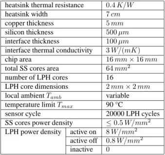
For simulating temperature, we used the ATMI model [22]. Our simulation parameters are listed in Table 4. We modeled LPH cores as squares with a uniform power density. The power density in the active LPH core is very high but notice that the whole SACC consumes “only”32 W , i.e., half the total power.
We assume that the SACC is designed for an ambient temperature not exceeding 40°C, i.e., we have chosen the heatsink thermal resistance value so that, when the migration interval is short enough, the average temperature in LPH cores is approximately 90 °C with a local ambient temperature6of 40 °C. Note that if we disabled migration and kept executing on the same core, temperature in the active core would exceed 170 °C.
When simulating the impact of thermal throttling, the initial thermal state may have a large impact on performance. Because our simulations are short (only 1 billion instructions), we want the initial thermal state to be as close as possible to the steady state. In the ATMI model, the initial thermal state is set indirectly : it is the steady-state corresponding to some specified power densities. To set the initial thermal state, we must determine approximately the power densities generated by long-term thermal throttling. We start from a uniform power density of0.5 W/mm2in all cores (including SS cores), and we compute the corresponding steady-state temperatures. If the hottest core is hotter thanTmax, we decrease the power
density in that core by a tiny amount. We iterate this process (the hottest core may change as we iterate) until the steady-state temperature is less than or equal toTmax in all cores. We use the resulting power
densities to initialize the thermal state.
Performance depends on ambient temperature. With sensor-less migrations and under normal thermal conditions, performance does not depend on the ambient temperature. This is no longer the case with sensor-triggered migrations. The migration interval depends not only on the ambient temperature but also
5In practice, power density is not uniform and depends on applications characteristics, which necessitates several sensors per core. 6The local ambient temperature is the temperature inside the computer case, at the CPU fan inlet. It is typically several degrees
heatsink thermal resistance 0.4 K/W
heatsink width 7 cm
copper thickness 5 mm
silicon thickness 500 µm
interface thickness 100 µm
interface thermal conductivity 3 W/(mK)
chip area 16 mm × 16 mm
total SS cores area 64 mm2
number of LPH cores 16
LPH core dimensions 2 mm × 2 mm
local ambientTamb variable
temperature limitTmax 90 °C
sensor cycle 20000 LPH cycles
SS cores power density ≤0.5 W/mm2
LPH power density active on 8 W/mm2
active off 0.8 W/mm2
inactive 0
Table 4: Thermal and physical parameters
0 0.1 0.2 0.3 0.4 0.5 0.6 0.7 0.8 0.9 1
Lag-0 WU-0 Lag-0 WU-1 Lag-0 WU-0 Lag-0 WU-1 Lag-0 WU-0 Lag-0 WU-1
Tamb=40 Tamb=45 Tamb=50
p e rf o rm a n c e tmin=50k tmin=100k tmin=200k tmin=500k tmin=1M tmin=10M
Figure 7: Harmonic mean of the normalized performance for Tamb = 40, 45, 50 °C and tmin =
50k, 100k, 200k, 500k, 1M, 10M core cycles.
on the heatsink temperature, i.e., what applications have been running previously. Of course, we expect migrations to have little impact under normal thermal conditions. But it will be almost impossible to replay the same program and get exactly the same execution time. Note however that this is already very difficult to achieve on current systems that are supposedly deterministic.
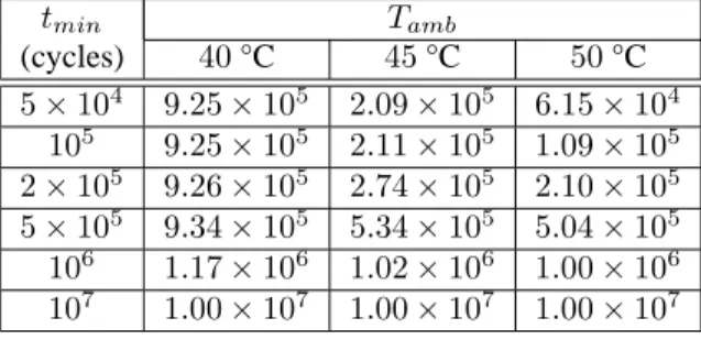
Results. Our simulation results are summarized in Figure 7, which shows the normalized performance for different values oftminandTamb. Table 5 gives the average migration interval in cycles.
WhenTamb = 40 °C, performance is within 10% of the maximum performance for most benchmarks,
providedtmindoes not exceed a few hundred thousand cycles. Lag-0 WU-1 is only 3% better than Lag-0
tmin Tamb (cycles) 40 °C 45 °C 50 °C 5 × 10⁴ 9.25 × 10⁵ 2.09 × 10⁵ 6.15 × 10⁴ 105 9.25 × 10⁵ 2.11 × 10⁵ 1.09 × 10⁵ 2 × 10⁵ 9.26 × 10⁵ 2.74 × 10⁵ 2.10 × 10⁵ 5 × 10⁵ 9.34 × 10⁵ 5.34 × 10⁵ 5.04 × 10⁵ 106 1.17 × 10⁶ 1.02 × 10⁶ 1.00 × 10⁶ 107 1.00 × 10⁷ 1.00 × 10⁷ 1.00 × 10⁷
Table 5: Average migration interval in cycles.
76 78 80 82 84 86 88 90 92 0.06 0.065 0.07 0.075 0.08 0.085 0.09 temperature (Celsius) time (seconds) core #5 core #6
Figure 8: Temperature on cores #5 and #6 as a function of time forTamb= 40 °C and tmin= 107cycles.
It must be noted thattmin = 107cycles gives a very low performance, even atTamb = 40 °C. As an
illustration, Figure 8 shows temperature on cores #5 and #6 as a function of time for one benchmark. The thermal limit of 90 °C is clearly underexploited. For large values oftmin, it takes a long time before the
execution revisits the same core again. When this time is long enough for temperature to drop significantly belowTmax, the time-averaged temperature is significantly lower thanTmax. As time-averaged temperature
relative toTamb is proportional to power, the total power that can be dissipated is smaller for large values
oftmin, and throttling triggers more often.
As the ambient temperature increases above 40 °C, the migration interval tends to decrease and the difference between Lag-0 WU-0 and Lag-0 WU-1 becomes more significant. AtTamb = 50 °C and for
tmin= 100k, Lag-0 WU-1 is on average 7% faster than Lag-0 WU-0 (up to 24% on one benchmark).
For very small values oftmin andTamb above 40 °C, the migration interval is small, so the
temper-ature oscillation on each core has a small amplitude and the time-averaged tempertemper-ature is close toTmax.
However, in this case, it is the migration penalty that limits performance. Consequently, for a given value ofTamb, there exists an optimal value oftmin. For instance, forTamb = 50 °C, the optimal value of tmin
seems to be around 100k cycles on average.
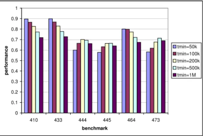
Actually, if we look at benchmarks individually, the optimal value oftmin is variable and depends
on the migration penalty, which depends on application characteristics. Figure 9 shows the normalized performance for Lag-0 WU-1 on a few benchmarks whenTamb = 50 °C. Setting tmin to 100k cycles
0 0.1 0.2 0.3 0.4 0.5 0.6 0.7 0.8 0.9 1 410 433 444 445 464 473 benchmark p e rf o rm a n c e tmin=50k tmin=100k tmin=200k tmin=500k tmin=1M
Figure 9: Normalized performance for Lag-0 WU-1 and various values oftmin on a subset of the
bench-marks whenTamb = 50 °C.
In summary, the SACC will provide maximum performance as long as the ambient temperature does not exceed a certain value. However, above this ambient temperature, each extra degree Celsius will decrease performance significantly. This problem can be solved by using dynamic voltage/frequency scaling (DVFS). It is not clear to what extent it will be possible to use fine-grained DVFS with migration intervals as short as those shown in Table 5. The advantage of linear throttling is that it reacts quickly, which is important for a sensor-triggered migration scheme because the high power density in the active core makes temperature increase very fast. Nevertheless, coarse-grained DVFS can be combined with linear throttling, i.e., voltage and frequency are adjusted automatically, but slowly, to maintain the fraction of linear throttling below a certain value. This should be an effective approach, as the ambient and heatsink temperatures vary slowly in general.
Unlike the case of sensor-less migration, where Lag-0 WU-1 brings a clear benefit, Lag-0 WU-0 is prob-ably sufficient for sensor-triggered migrations. Lag-0 WU-1 brings a performance gain when the ambient temperature is high. But when the ambient temperature is normal, L2 warm-up is superfluous.
6.4
Remarks
We have assumed a 8 GHz clock frequency for the LPH core, which may be pessimistic in 11 nm technol-ogy. We also ran some simulations assuming a 16 GHz clock frequency (with the bus still at 500 MHz). Apart from the higher average performance, this did not change our qualitative conclusions. Actually, the relative migration penalty is on average slightly smaller with a higher frequency.
We assumed that the power consumption of inactive cores is much smaller than the power consumption in the active core. If this is not true, the power budget that can be allotted to the active core is reduced, and the LPH core design and/or the voltage/frequency setting will be less aggressive.
Another pessimistic assumption is to simulate the same power density for all the applications. Actually, the power consumption depends on the application characteristics. The design, voltage and frequency setting of the LPH core will be based on typical “hot” applications. With sensor-triggered migration, “cold” applications will experience longer migration intervals due to their lower power density.
In this study, we have assumed that all cores are functioning correctly. In practice, because of transistor variability, there may be some malfunctioning LPH cores detected at manufacturing time. The SACC control must be programmed at manufacturing time so that invalid cores are removed from the migration path. When this happens, the SACC area and power envelope are reduced, which means a lower voltage and clock frequency.
7
Conclusion
We believe that, on future general-purpose manycore processors, a large part of the chip area should be dedicated to high sequential performance. Microarchitecture and circuit design solutions that are deemed too power hungry today may become viable in a few technology generations and will allow to maximize sequential performance. Based on this assumption, we have proposed a sequential accelerator consisting of several large hungry cores where a single core is active at a given time and other cores are power-gated. Periodically, the execution is migrated to a new active core in order to spread the heat generation uniformly over the whole accelerator area.
We emphasized in this study the importance of not ignoring the potential impact of migration-induced L2 misses on performance. We proposed and evaluated some schemes for decreasing this impact. We made a case for write-through level-2 caches and write-back level-1 data caches. We also showed that, when LPH cores are connected by a slow shared bus, warming-up the L2 cache of future cores on which we are going to migrate is more interesting than fetching blocks from past cores. We showed that L2 warm-up brings a significant performance gain for a sensor-less migration scheme.
We also proposed a sensor-triggered migration method which ensures that the migration interval is not smaller than a fixed minimum. As long as the ambient temperature stays below the targeted value, migrations incur little performance loss. However, when the ambient temperature exceeds that value , performance degrades significantly if linear throttling is the only throttling method implemented.
Overall, our study stresses the importance for microarchitects to keep searching ways to improve se-quential performance, even if power-hungry solutions are necessary to achieve this goal. Nevertheless, the success of our proposition will depend on the effectiveness of power-gating techniques.
8
Acknowledgments
This work was partially supported by the European Commission in the context of the SARC integrated project #27648 (FP6).
References
[1] M. Annavaram, E. Grochowski, and J. Shen. Mitigating Amdahl’s law through EPI throttling. In Proceedings of the 32nd Annual International Symposium on Computer Architecture, 2005.
[2] S. Balakrishnan, R. Rajwar, M. Upton, and K. Lai. The impact of performance asymmetry in emerging multicore architectures. In Proceedings of the 32nd Annual International Symposium on Computer Architecture, 2005.
[3] J.A. Brown and D.M. Tullsen. The shared-thread multiprocessor. In Proceedings of the International Conference on Supercomputing, 2008.
[4] P. Chaparro, J. Gonz´alez, G. Magklis, Q. Cai, and A. Gonz´alez. Understanding the thermal implica-tions of multicore architectures. IEEE Transacimplica-tions on Parallel and Distributed Systems, 18(8):1055– 1065, August 2007.
[5] B. Choi, L. Porter, and D.M. Tullsen. Accurate branch prediction for short threads. In Proceed-ings of the 13th International Conference on Architectural Support for Programming Languages and Operating Systems, 2008.
[6] T. Constantinou, Y. Sazeides, P. Michaud, D. Fetis, and A. Seznec. Performance implications of single thread migration on a chip multi core. ACM SIGARCH Computer Architecture News, 33(4):80–91, November 2005.
[7] J. Donald and M. Martonosi. Techniques for multicore thermal management : classification and new exploration. In Proceedings of the 33rd Annual International Symposium on Computer Architecture, 2006.
[8] S.H. Gunther, F. Binns, D.M. Carmean, and J.C. Hall. Managing the impact of increasing micropro-cessor power consumption. Intel Technology Journal, (Q1), February 2001.
[9] L. Hammond, B.A. Hubbert, M. Siu, M.K. Prabhu, M.K. Chen, and K. Olukotun. The Stanford Hydra CMP. IEEE Micro, 20(2):71–84, March 2000.
[10] S. Heo, K. Barr, and K. Asanovi´c. Reducing power density through activity migration. In Proceedings of the International Symposium on Low Power Electronics and Design, 2003.
[11] M.D. Hill and M.R. Marty. Amdahl’s law in the multicore era. Technical Report CS-TR-2007-1593, University of Wisconsin, April 2007.
[12] Intel. Intel Core i7 Extreme Edition and Intel Core i7 Processor and LGA1366 Socket, Thermal / Mechanical Design Guide, March 2009. Section 5.3.1.
[13] E. ˙Ipek, M. Kırman, N. Kırman, and J.F. Mart´ınez. Core fusion : accommodating software diversity in chip multiprocessors. In Proceedings of the International Symposium on Computer Architecture, 2007.
[14] U.R. Karpuzcu, B. Greskamp, and J. Torrellas. The BubbleWrap many-core : popping cores for sequential acceleration. In Proceedings of the International Symposium on Microarchitecture, 2009. [15] C. Kim, S. Sethumadhavan, M.S. Govindan, N. Ranganathan, D. Gulati, D. Burger, and S.W. Keckler.
Composable lightweight processors. In Proceedings of the International Symposium on Microarchi-tecture, 2007.
[16] N.S. Kim, K. Flautner, D. Blaauw, and T. Mudge. Circuit and microarchitectural techniques for reducing cache leakage power. IEEE Transactions on Very Large Scale Integration (VLSI) Systems, 12(2):167–184, January 2004.
[17] V. Krishnan and J. Torrellas. A chip-multiprocessor architecture with speculative multithreading. IEEE Transactions on Computers, 48(9):866–880, September 1999.
[18] R. Kumar and G. Hinton. A family of 45nm IA processors. In IEEE International Solid-State Circuits Conference Digest of technical papers, 2009.
[19] R. Kumar, D.M. Tullsen, N.P. Jouppi, and P. Ranganathan. Heterogeneous chip multiprocessors. IEEE Computer, 38(11):32–38, November 2005.
[20] C.H. Lim, W.R. Daasch, and G. Cai. A thermal-aware superscalar microprocessor. In Proceedings of the International Symposium on Quality Electronic Design, 2002.
[21] C.-K. Luk, R. Cohn, R. Muth, H. Patil, A. Klauser, G. Lowney, S. Wallace, V. Janapa Reddi, and K. Hazelwood. Pin : building customized program analysis tools with dynamic instrumentation. In Proceedings of the ACM SIGPLAN conference on Programming Language Design and Implementa-tion, 2005.
[22] P. Michaud and Y. Sazeides. ATMI: analytical model of temperature in microprocessors. In Third Annual Workshop on Modeling, Benchmarking and Simulation, 2007.
[23] P. Michaud, Y. Sazeides, A. Seznec, T. Constantinou, and D. Fetis. An analytical model of temperature in microprocessors. Research report RR-5744, INRIA, November 2005.
[24] P. Michaud, Y. Sazeides, A. Seznec, T. Constantinou, and D. Fetis. A study of thread migration in temperature-constrained multicores. ACM Transactions on Architecture and Code Optimization, 4(2), June 2007.
[25] T.Y. Morad, U.C. Weiser, A. Kolodny, M. Valero, and E. Ayguad´e. Performance, power efficiency and scalability of asymmetric cluster chip multiprocessors. IEEE Computer Architecture Letters, 5(1), June 2006.
[26] D. Pham et al. The design methodology and implementation of a first-generation CELL processor : a multi-core SoC. In Proceedings of the IEEE Custom Integrated Circuits Conference, 2005.
[27] M.D. Powell, M. Gomaa, and T.N. Vijaykumar. Heat-and-run: leveraging SMT and CMP to manage power density through the operating system. In Proceedings of the 11th International Conference on Architectural Support for Programming Languages and Operating Systems, 2004.
[28] K.K. Rangan, G.-Y. Wei, and D. Brooks. Thread motion : fine-grained power management for multi-core systems. In Proceedings of the International Symposium on Computer Architecture, 2009. [29] A. Shayesteh, E. Kursun, T. Sherwood, S. Sair, and G. Reinman. Reducing the latency and area cost
of core swapping through shared helper engines. In Proceedings of the International Conference on Computer Design, 2005.
[30] K. Skadron, M.R. Stan, W. Huang, S. Velusamy, K. Sankaranarayanan, and D. Tarjan. Temperature-aware microarchitecture. In Proceedings of the 30th Annual International Symposium on Computer Architecture, 2003.
[31] G.S. Sohi, S. Breach, and T.N. Vijaykumar. Multiscalar processors. In Proceedings of the 22nd Annual International Symposium on Computer Architecture, 1995.
[32] B. Stolt, Y. Mittlefehldt, S. Dubey, G. Mittal, M. Lee, J. Friedrich, and E. Fluhr. Design and im-plementation of the POWER6 microprocessor. IEEE Journal of Solid-State Circuits, 43(1):21–28, January 2008.
[33] M.A. Suleman, O. Mutlu, M.K. Qureshi, and Y.N. Patt. Accelerating critical section execution with asymmetric multi-core architectures. In Proceedings of the 14th International Conference on Archi-tectural Support for Programming Languages and Operating Systems, 2009.
[34] J.W. Tschanz, S.G. Narendra, Y. Ye, B.A. Bloechel, S. Borkar, and V. De. Dynamic sleep transistor and body bias for active leakage power control of microprocessors. IEEE Journal of Solid-State Circuits, 38(11):1838–1845, November 2003.
Centre de recherche INRIA Bordeaux – Sud Ouest : Domaine Universitaire - 351, cours de la Libération - 33405 Talence Cedex Centre de recherche INRIA Grenoble – Rhône-Alpes : 655, avenue de l’Europe - 38334 Montbonnot Saint-Ismier Centre de recherche INRIA Lille – Nord Europe : Parc Scientifique de la Haute Borne - 40, avenue Halley - 59650 Villeneuve d’Ascq
Centre de recherche INRIA Nancy – Grand Est : LORIA, Technopôle de Nancy-Brabois - Campus scientifique 615, rue du Jardin Botanique - BP 101 - 54602 Villers-lès-Nancy Cedex
Centre de recherche INRIA Paris – Rocquencourt : Domaine de Voluceau - Rocquencourt - BP 105 - 78153 Le Chesnay Cedex Centre de recherche INRIA Saclay – Île-de-France : Parc Orsay Université - ZAC des Vignes : 4, rue Jacques Monod - 91893 Orsay Cedex
Centre de recherche INRIA Sophia Antipolis – Méditerranée : 2004, route des Lucioles - BP 93 - 06902 Sophia Antipolis Cedex
Éditeur