HAL Id: hal-00711315
https://hal.archives-ouvertes.fr/hal-00711315
Submitted on 23 Jun 2012
HAL is a multi-disciplinary open access
archive for the deposit and dissemination of
sci-entific research documents, whether they are
pub-lished or not. The documents may come from
teaching and research institutions in France or
abroad, or from public or private research centers.
L’archive ouverte pluridisciplinaire HAL, est
destinée au dépôt et à la diffusion de documents
scientifiques de niveau recherche, publiés ou non,
émanant des établissements d’enseignement et de
recherche français ou étrangers, des laboratoires
publics ou privés.
Hardware Simulator: Digital Block Design for
Time-Varying MIMO Channels with TGn Model B Test
Bachir Habib, Gheorghe Zaharia, Ghaïs El Zein
To cite this version:
Bachir Habib, Gheorghe Zaharia, Ghaïs El Zein. Hardware Simulator: Digital Block Design for
Time-Varying MIMO Channels with TGn Model B Test. International Conference on Telecommunications,
Apr 2012, Jounieh, Lebanon. pp.1-5, �10.1109/ICTEL.2012.6221269�. �hal-00711315�
Hardware Simulator: Digital Block Design for
Time-Varying MIMO Channels with TGn Model B Test
Bachir Habib, Gheorghe Zaharia, Ghaïs El Zein
IETR - Institut d’Electronique et de Télécommunications de Rennes - UMR CNRS 6164 20 av. des Buttes de Coësmes, CS 70839 - 35708, Rennes cedex 7, France
Abstract—A hardware simulator facilitates the test and validation
cycles by replicating channel artifacts in a controllable and repeatable laboratory environment. Thus, it makes possible to ensure the same test conditions in order to compare the performance of various equipments. This paper presents new frequency domain and time domain architectures of the digital block of a hardware simulator of MIMO propagation channels. The two architectures are tested with WLAN 802.11ac standard, in indoor environment, using time-varying TGn 802.11n channel model B. After the description of the general characteristics of the hardware simulator, the new architectures of the digital block are presented and designed on a Xilinx Virtex-IV FPGA. Their accuracy and latency are analyzed.
Keywords-Hardware simulator; radio channel; MIMO; FPGA; Time-varying TGn channel model B; 802.11ac
I. INTRODUCTION
Hardware simulators of mobile radio channel are very useful for the test and verification of wireless communication systems. These simulators are standalone units that provide the fading signal in the form of analog or digital samples [1], [2].
The current communication standards indicate a clear trend in industry toward supporting Input Multiple-Output (MIMO) functionality. In fact, several studies published recently present systems that reach an order of 8×8 and higher [3]. This is made possible by advances at all levels of the communication platform, as the monolithic integration of antennas [4] and the design of the simulator platforms.
With the continuous increase of field programmable gate array (FPGA) capacity, entire baseband systems can be efficiently mapped onto faster FPGAs for more efficient testing and verification. As shown in [5], the FPGAs provide the greatest flexibility in algorithm design. Also, they are ideal for rapid prototyping and research use such as testbed [6].
The simulator is reconfigurable with standard bandwidths not exceeding 100 MHz (the maximum value for FPGA Virtex-IV). However, in order to exceed 100 MHz bandwidth, more performing FPGA as Virtex-VII can be used [7]. The simulator is configured with the Long Term Evolution System (LTE) and Wireless Local Area Networks (WLAN) 802.11ac standards. The channel models used by the simulator can be obtained from standard channel models, as the TGn 802.11n [8] and 3GPP TR 36.803 [9] models, or from real
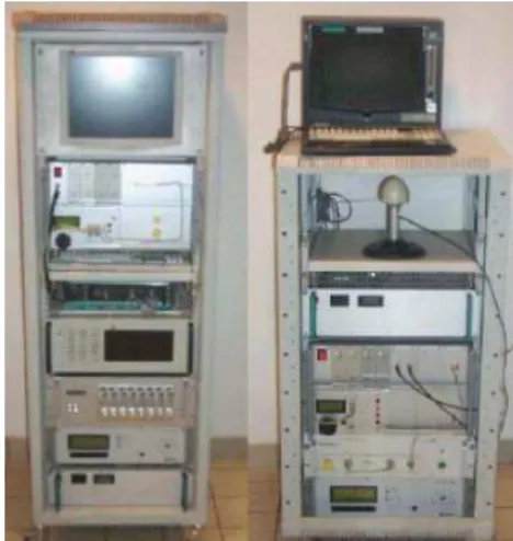
measurements by using a time domain MIMO channel sounder designed and realized at IETR [10], [11], as shown in Fig. 1.
Figure 1. MIMO channel sounder: receiver (left) and transmitter (right).
At IETR, several architectures of the digital block of a hardware simulator have been studied, in time and frequency domains [12], [13]. Moreover, a new method based on determining the parameters of the simulator by fitting the space time-frequency cross-correlation matrix to the estimated matrix of a real-world channel was presented in [14]. This solution shows that the error can be important. Typically, wireless channels are commonly simulated using finite impulse response (FIR) filters, as in [13], [15] and [16]. However, for a hardware implementation, it is easier to use the FFT (Fast Fourier Transform) module to obtain an algebraic product. Thus, frequency architectures are proposed, as in [12] and [14]. The previous considered frequency architectures operate correctly only for signals with a number of samples not exceeding the size of the FFT. Therefore, in this paper, a new frequency domain architecture avoiding this limitation, and a new time domain architecture are both tested with time-varying TGn 802.11n channel model B.
The rest of this paper is organized as follows. Section II presents the architectures of the digital block. Section III describes their hardware implementation. Moreover, the accuracy of these two architectures is analyzed. Lastly,
Sections IV and V present a discussion and a conclusion.
II. HARDWARE SIMULATOR:PRINCIPLE,ARCHITECTURE AND OPERATION
The design of the RF blocks for UMTS (Universal Mobile Telecommunications System) standard was completed during a
previous project [12], [13]. PALMYRE II* project mainly
concerns the channel models and their hardware
implementation into the MIMO simulator.
A. Standard TGn Channel Models
The standard TGn [8] has a set of 6 channel models, labeled A to F, which cover all the scenarios for indoor environments.
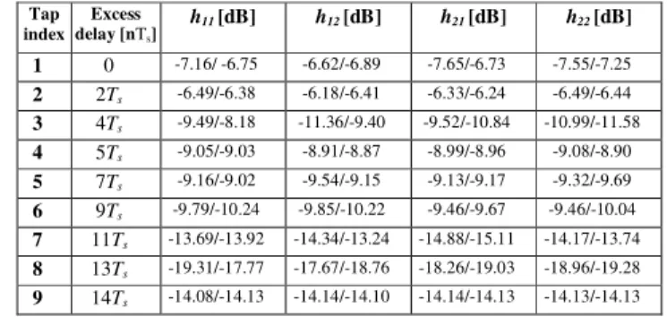
Model B is used for residential indoor environments and it is presented in details in [8]. Table I summaries the average relative power (RP) of each tap for model B by taking the direct path as a reference. For 802.11ac, the sampling
frequency fs= 180 MHz and Ts = 1/fs.
TABLE I. AVERAGE RELATIVE POWER OF EACH TAP FOR MODEL B
Tap index 1 2 3 4 5 6 7 8 9 Excess delay [nTs] 0 2Ts 4Ts 5Ts 7Ts 9Ts 11Ts 13Ts 14Ts
RP [dB] 0 -5.4 -2.5 -5.87 -9.15 -12.5 -15.6 -18.7 -21.8
RP [linear] 1 0.288 0.561 0.258 0.121 0.056 0.027 0.013 0.006
B. Time-Varying TGn Channel Model B
In the MIMO context, little experimental results have been obtained regarding time-variations, partly because of limitations in channel sounding equipment [17].
The intent of the Doppler model in the IEEE 802.11n channel model was to simulate an indoor home or office environment in which the wireless devices are stationary but the channel is dynamic due to the people moving in the environment [8]. This explicitly differs from outdoor mobile systems where the user terminal is typically moving.
The 802.11n channel model B for MIMO 2×2 uses a Bell shaped normalized Doppler spectrum defined by:
=
. . 1 + . 1
where S(f) is expressed in linear scale and each receive antenna
is assigned half the power. is the Doppler spread. A is a
constant, used to obtain S( )= 0.1. Thus, A = 9. At a center
frequency of 5 GHz and an environmental speed at 1.2 km/h, = 6 Hz.
The autocorrelation function of the Bell shape is given by:
= . .
. . .∆ !
2
Therefore, from R(Tc)/R(0) = 1/2, the coherence time is:
#$= 2. . .%& 2 3
This model yields a coherence time of approximately 55
ms. Thus, the refresh frequency is chosen fref = 18.18 Hz.
To vary the channel, a solution in [20] is proposed. It defines:
ℎ = )*)+,ℎ-& ./, .1, #2, 3, 45, 22 3 %-6, 7839: 4 where h constructs a MIMO Rayleigh fading channel object.
Nt = 2 is the number of transmit antennas. Nr = 2 is the number
of receive antennas.
The gain and phase elements of a channel's distortion are represented as a complex number. thus, Rayleigh fading assume that the real and imaginary parts of the response are modeled by independent and identically distributed zero-mean Gaussian processes so that the amplitude of the response is the sum of two such processes.
In our case, it is simply the amplitude fluctuations that are of interest. Our goal is to produce a signal that has S(f) given in (1) and the equivalent properties of R given in (2).
The model for the Rayleigh fading is proposed in [21] and it
is based on summing sinusoids. The Rayleigh fading of the kth
waveform over time t is modeled by:
/, < = 2 2 => ?+2@A+ B2*&@A ,+2C2 / + DA,EF
G AHI
+ ,+2 2
2 / J 5
where M = 2. @A chosen so that there is no cross-correlation
between the real and imaginary parts of /, < :
@
&=L + 1 6&D
&,< is used to generate multiple waveforms. Moreover, for uncorrelated waveforms it is given by:D
&,<=@
&+2
L + 1 7< − 1 In this paper, we simulate and analyze two successive 2×2 MIMO profiles: pack1 and pack2. Table II presents the relative power of the two successive packs for the four sub-channelsimpulse responses: h11, h12, h21, h22, using time-varying TGn
channel model B, with fref = 18.18 Hz between the two
successive packs.
TABLE II. RELATIVE POWER OF TWO PACKS OF MIMO2X2IMPULSE
RESPONSES:PACK1/PACK2
Tap index Excess delay [nTs] h11 [dB] h12 [dB] h21 [dB] h22 [dB] 1 0 -7.16/ -6.75 -6.62/-6.89 -7.65/-6.73 -7.55/-7.25 2 2Ts -6.49/-6.38 -6.18/-6.41 -6.33/-6.24 -6.49/-6.44 3 4Ts -9.49/-8.18 -11.36/-9.40 -9.52/-10.84 -10.99/-11.58 4 5Ts -9.05/-9.03 -8.91/-8.87 -8.99/-8.96 -9.08/-8.90 5 7Ts -9.16/-9.02 -9.54/-9.15 -9.13/-9.17 -9.32/-9.69 6 9Ts -9.79/-10.24 -9.85/-10.22 -9.46/-9.67 -9.46/-10.04 7 11Ts -13.69/-13.92 -14.34/-13.24 -14.88/-15.11 -14.17/-13.74 8 13Ts -19.31/-17.77 -17.67/-18.76 -18.26/-19.03 -18.96/-19.28 9 14Ts -14.08/-14.13 -14.14/-14.10 -14.14/-14.13 -14.13/-14.13
01010011001100 N = 14 bits M = 17 bits 12 bits 12 bits 12 bits 16 bits 16 bits 12 bits 17 bits 16 bits 16 bits 16 bits 9 of 14 9 of 14 14 bits 16 bits 16 bits 1 2 9 35 bits 14 bits t=0 t=tp 14 bits 14 bits 16 bits C. Digital Block
According to the considered propagation environments, Table III summarizes some useful parameters for WLAN 802.11ac standard.
TABLE III. SIMULATION PARAMETERS
Type Cell Size Wt eff (PQ N Wt (PQ
Office Indoor Outdoor 40 m 50-150 m 50-150 m 0.35 0.71 1.16 64 128 256 0.35 0.71 1.42
Wt eff represents the width of the time window of the MIMO
impulse responses. The number of samples is:
. = R. S T
where Wt is the closest value for Wt eff which is imposed by
N = 2n which is the size of the FFT module.
In order to have a suitable trade-off between complexity and latency, two solutions are considered: a time domain approach and a frequency domain approach. For indoor
environments Wt is smaller than 1 UV. Therefore, the time
domain approach is more suitable to use, because a FIR filter has, in spite of its relative complexity, much lower latency. However, the frequency approach has huge generated latency
(more than 1UV). Therefore, both approaches can be used
according to the considered propagation environment.
A description of the architecture of the digital block for “simple” frequency and time domains is presented in [12] and [13], which is also simulated and tested. In this section, we present a new and improved frequency domain architecture and a time domain architecture based on a FIR filter.
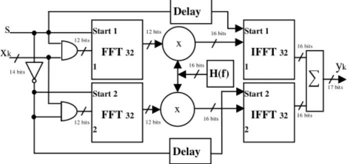
1) New Frequency Domain Architecture
The new frequency architecture presented in Fig. 2 has been verified with Gaussian impulse response [18]. It operates correctly for signals with a number of samples exceeding N,
where N = 2n is the size of the FFT module.
For TGn model B, the largest excess delay is 14 samples. Thus, N = 16 samples. However, it is mandatory to extend each partial input of N samples with a “tail” of N null samples, as presented in [18], to avoid a wrong result. Therefore, the FFT/IFFT modules operate with 32 samples.
Figure 2. Frequency architecture for a SISO channel.
Due to the use of a 14-bit digital-to-analog convertor (DAC), the output of the final adder must be truncated. A simple solution is to keep the 14 most significant bits. This is a
“brutal” truncation. However, for small values of the output of the digital adder, the brutal truncation generates zero values to the input of the DAC. Therefore, a better solution is the sliding window truncation presented in Fig. 3 which uses the 14 most effective significant bits.
Figure 3. Sliding window truncation, from 17 to 14 bits.
2) Time Domain Architecture
Studies of the FIR filter with 64 points are presented in [13]. However, for TGn model B, N = 14 samples and only 9 multipliers are necessary. The general formula for a FIR 14 with 9 multipliers is:
6W * = > ℎW *E . 5W * − *E , * X .
Y EHI
Z The index q suggests the use of quantified samples and
hq(ik) is the attenuation of the kth path with the delay ikTs. Fig. 4
presents the architecture of the FIR filter 14 with 9 non-null coefficients. This architecture uses series of impulse responses in order to simulate a time variant channel. Therefore, we have developed our own FIR filter instead of using Xilinx MAC FIR filter to make it possible to reload the FIR filter coefficients.
Figure 4. FIR filter14 with 9 multipliers for a SISO channel.
III. IMPLEMENTATION AND TESTS
In order to implement the hardware simulator, the adopted
solution uses a prototyping platform (XtremeDSP
Development Kit-IV for Virtex-IV) from Xilinx [7], which is presented in Fig. 5 and described in [18].
Figure 5. XtremeDSP Development board Kit-IV for Virtex-IV.
00010100110011000 Truncation CNA yk s 14 bits xk Start 1 FFT 32 1 Start 2 FFT 32 2 Delay Start 1 IFFT 32 1 Start 2 IFFT 32 2 x x H(f) > Delay
n(i) n(i-1) n(i-2) --- n(i-13)
>
h(0) h(1) h(2) --- h(13)
The simulations and synthesis are made with Xilinx ISE [7] and ModelSim software [19].
A. Implementation and Results of the Frequency Architecture
As a development board has 2 ADC and 2 DAC, it can be connected to only 2 down-conversion RF units and 2 up conversion RF units. Therefore, 4 frequency architectures are needed to simulate a one-way 2 x 2 MIMO radio channel. They are implemented in the digital block of the FPGA. The channel frequency response profiles are stored on the hard disk of the computer and read via the PCI bus then they are stored in the FPGA dual-port RAM. Fig. 6 shows the connection between the computer and the FPGA board to reload the coefficients.
Figure 6. Connection between the computer and the XtremeDSP board.
For 802.11ac standard, fref is 18.18 Hz and the refreshing
period is approximately 55 ms during which we must change the four profiles. For one MIMO profile, (32+1).4 = 132 words of 32 bits = 528 bytes is transmitted. Therefore the data rate is: 528/(55ms) = 9.6 KB/s. The PCI bus is chosen to load the profiles of frequency responses. It has a speed up to 30 MB/s.
The V4-SX35 utilization summary is given in Table IV for four frequency architecture with their additional circuits used to dynamically reload the channel coefficients.
TABLE IV. VIRTEX-IVSX35UTILIZATION FOR FOUR SISO CHANNELS
USING THE FREQUENCY DOMAIN ARCHITECTURE
Number of slices Number of bloc RAM Number of multiplier 9,825 out of 15,360 93 out of 192 127 out of 192 64 % 49 % 66 %
In order to determine the accuracy of the digital block, a comparison is made between the theoretical signal and the Xilinx output signal. With Gaussian input signal, the theoretic output signal can be easily obtained. Thus the accuracy of the Xilinx signal can be calculated. Therefore, an input Gaussian signal x(t) is considered and long enough to be used in
streaming mode (a length of 3Wt is sufficient):
5 / = 5[
\]^_
` , a b / b 3R
1a
where N = 32, Wt= NTs, mx = 21Ts and σ = mx/4.
For TGn model B with time-varying channel, each impulse response has 9 paths. The A/D and D/A convertors of the
development board have a full scale [-Vm,Vm], with Vm = 1 V.
For the simulations we consider xm = Vm/2. The theoretical
output signal is:
6 / = cYEHIℎ *E . 5 / − *E#S (11)
The relative error is computed for each output sample by: d * = e_fgfh_i e\jklmni
e\jklmni . 1aa 8o: 12
where YXilinx and Ytheory are vectors containing the samples of
corresponding signals. The Signal-to-Noise Ratio (SNR) is:
SNR * = 20. %+pIqre_fgfh_e\jklmni e\jklmni ir 839: , * = 1, 3. + stttttttttttttY 13
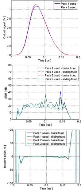
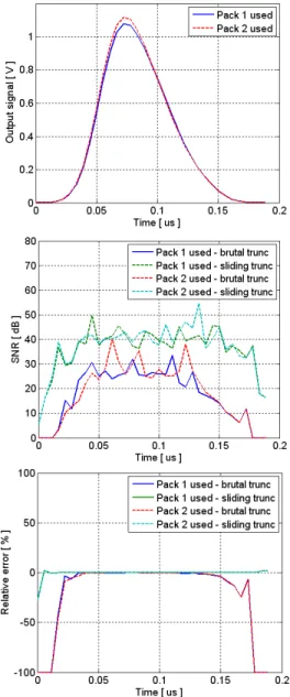
Fig. 7 presents the Xilinx output signal, the SNR and the
relative error with 802.11ac signals (fs= 180 MHz), using four
frequency architectures, for the two successive packs for the four impulse responses (2×2 MIMO channels).
Figure 7. The Xilinx output signals for frequency domain architecture, the SNR and the relative error.
After the D/A convertor, the signal is limited to [-Vm,Vm]
with Vm = 1. If ymax > 1 V as shown in Fig. 8, a reconfigurable
Spatan II Virtex IV XtremeDSP Board Computer Driver Nallatech Profiles File PCI Interface Digital Block Host Interface Loading Profiles
analog amplifier placed after the DAC must multiply the signal
with 2Eu, where k0 is the smallest integer verifying ymax < 2Eu.
The relative error is high only for small values of the output signal because the Gaussian signal test is close to 0.
B. Implementation and Results of Temporal Architecture
For the time domain architecture, the amount of data transmit for a profile is: (9+1).4 = 40 words of 16 bits = 80 bytes. Therefore, the data rate is: 80/(55ms) = 1.45 KB/s.
Fig. 8 presents the Xilinx output signal, the SNR and the
relative error with with 802.11ac signals (fs= 180 MHz), using
four FIR filters with 14 taps and 9 multipliers, for the two successive packs for the four impulse responses (2×2 MIMO channels) of TGn time-varying channel model B.
Figure 8. The Xilinx output signals for time domain architecture, the SNR and the relative error.
Table V shows the FPGA utilization for four FIR filters with their additional circuits used to dynamically reload the channel coefficients, in one V4-SX35.
TABLE V. FIR SIMULATED ARCITECTURE
Number of slices Number of bloc RAM Number of multiplier 6,909 out of 15,360 36 out of 192 36 out of 192 45 % 19 % 19 %
C. The Accuracy of the Architectures
The global values of the relative error and of the SNR of the output signal before and after the final truncation are necessary to evaluate the accuracy with the new architectures and the improvement obtained with the sliding truncation.
The global value of the relative error is computed by:
d =xevwv
\jklmnx. 1aa [%] (14)
and the global SNR is:
. y= 2a. %+pIqxe\jklmnvwv x [dB] (15)
where E = YXilinx- Ytheory is the error vector.
For a given vector X = [ x1 , x2, …, xL], its Euclidean norm
|| x || is:
v5v = zI{c{EHI5E (16)
Table VI shows the global values of the relative error and SNR for the considered impulse responses of TGn time-varying channel model B, using both frequency and time domain architectures. The results are given without truncation, with sliding window truncation and with brutal truncation, for the two successive packs.
TABLE VI. GLOBAL RELATIVE ERROR AND GLOBAL SNR
Frequency Architecture Time Architecture
Error (%) SNR (dB) Error (%) SNR (dB)
Without truncation
Pack 1 1.0121 39.85 0.0032 89.77
Pack 2 1.0610 39.43 0.0035 89.18
With sliding window truncation
Pack 1 1.4992 36.58 0.0129 77.78
Pack 2 1.3394 37.37 0.0096 80.36
With brutal truncation
Pack 1 1.5061 36.54 0.4194 47.52
Pack 2 1.3416 37.36 0.3772 48.45
IV. DISCUSSION
The goal is to compare the frequency architecture with the time domain architecture. Three points are considered: the precision, the FPGA occupation and the latency.
i. Precision
If we compare the outputs in Fig. 7 and Fig. 8, with frequency domain architecture and time domain architecture, we observe that:
1) For the frequency domain architecture with both sliding window truncation and brutal truncation, the greatest values of output voltage, i.e. values greater than 0.4 V, have a relative error less than 1 %.
2) For the time domain architecture with brutal truncation, the greatest values of output voltage, i.e. values greater than 0.35 V, have a relative error less than 1 %.
3) For the time domain architecture with sliding window
truncation, if the output voltage is greater than 0.01 V, then the relative error is less than 1 %.
We conclude that for the frequency domain architecture, the brutal truncation is more suitable to use because it is simpler to implement and gives almost the same result as the sliding window truncation. It offers a reduction of the complexity and the slice occupation on the FPGA. Moreover, it avoids the need of a reconfigurable analog amplifier after the DAC. However, for the time domain architecture, the sliding window truncation is more suitable to use because it reduces the error and make it possible use output signals as low as 0.01 V.
The global relative error presented in Table VI does not exceed 1.51 % (with the frequency domain architecture with brutal truncation), which is sufficient for the test. However, the time domain architecture presents higher precision (less than 0.02 % with sliding window truncation).
ii. FPGA Occupation
According to Tables IV and V, the time domain architecture presents a slice occupation of 45 % on the FPGA Virtex-IV, which is better than 64% the occupation of the frequency domain architecture.
Thus, the time domain architecture presents another advantage which allows the implementation of 8 SISO channels. Therefore, 4×2 MIMO channels can be implemented on a single Virtex-IV. In this case, 9×8 = 72 multipliers are needed and the slice occupation on the FPGA is 96 %.
iii. Latency
The time domain architecture presents another advantage by generating a latency of 125 ns for each simulated profile.
The new frequency architecture has a latency of 46 Us.
V. CONCLUSION
After a comparative study, in order to reduce the occupation on the FPGA, the error of the output signals and the latency of the digital block, the time domain architecture represents the best solution, especially for MIMO systems.
VI. PROSPECTS
Simulations and tests will be made with time-varying impulse responses for outdoor environments. Moreover, using
a Virtex-VII [7] XC7V2000T platform will allow us to simulate up to 12×12 MIMO channels. Measurement campaigns will also be carried with the MIMO channel sounder realized by IETR, for various types of environments. A Graphical User Interface will also be designed to allow the user to reconfigure the channel parameters. The final objective of this work is to simulate realistic impulse responses of the MIMO channels with different MIMO standards.
REFERENCES
[1] Wireless Channel Emulator, Spirent Communications, 2006.
[2] Baseband Fading Simulator ABFS, Reduced costs through baseband simulation, Rohde & Schwarz, 1999.
[3] A. S. Behbahani, R. Merched, and A. Eltawil, “Optimizations of a MIMO relay network,” IEEE Trans. on Signal Processing, vol. 56, no. 10, pp. 5062–5073, Oct. 2008.
[4] B. A. Cetiner, E. Sengul, E. Akay, and E. Ayanoglu, “A MIMO system with multifunctional reconfigurable antennas”, IEEE Antennas Wireless Propag. Lett., vol. 5, no. 1, pp. 463–466, Dec. 2006.
[5] P. Murphy, F. Lou, A. Sabharwal, P. Frantz, "An FPGA Based Rapid Prototyping Platform for MIMO Systems", Asilomar Conf. on Signals, Systems and Computers, ACSSC, Vol. 1, pp. 900-904, 9-12 Nov. 2003. [6] P. Murphy, F. Lou, J. P. Frantz, "A hardware testbed for the
implementation and evaluation of MIMO algorithms", Conf. on Mobile and Wireless Communications Networks, Singapore, 27-29 Oct. 2003. [7] "Xilinx: FPGA, CPLD and EPP solutions", www.xilinx.com.
[8] V. Erceg, L. Schumacher, P. Kyritsi, et al., “TGn Channel Models”, IEEE Tech. Rep. 802.11- 03/940r4, May 10, 2004.
[9] Agilent Technologies, “Advanced design system – LTE channel model - R4-070872 3GPP TR 36.803 v0.3.0”, 2008.
[10] G. El Zein, R. Cosquer, J. Guillet, H. Farhat, F. Sagnard, “Characterization and modeling of the MIMO propagation channel: an overview”, ECWT, Paris, 2005.
[11] H. Farhat, R. Cosquer, G. El Zein, "On MIMO channel characterization for future wireless communication systems", 4G Mobile & Wireless Comm.Tech., River Publishers, Aalborg, Denmark, 2008, pp. 225-233. [12] S. Picol, G. Zaharia, D. Houzetand G. El Zein, "Design of the digital
block of a hardware simulator for MIMO radio channels", IEEE PIMRC, Helsinki, Finland, 2006.
[13] S. Picol, G. Zaharia, D. Houzetand G. El Zein, "Hardware simulator for MIMO radio channels: Design and features of the digital block", Proc. of IEEE VTC-Fall 2008, 21-24 Sept. 2008, Calgary, Canada.
[14] D. Umansky, M. Patzold, "Design of Measurement-Based Stochastic Wideband MIMO Channel Simulators", IEEE Globecom 2009, Honolulu, Hawai, 30 Nov. - 4 Dec. 2009.
[15] H. Eslami, S.V. Tran and A.M. Eltawil, "Design and implementation of a scalable channel Emulator for wideband MIMO systems", IEEE Trans. on Vehicular Technology, vol. 58, no. 9, Nov. 2009, pp. 4698-4708. [16] S. Fouladi Fard, A. Alimohammad, B. Cockburn, C. Schlegel, "A single
FPGA filter-based multipath fading emulator", Globecom, Canada, 2009. [17] P. Almers, E. Bonek et al., "Survery of Channel and Radio Propagation
Models for Wireless MIMO Systems", EURASIP Journal on Wireless Communications and Networking, Volume 2007, Article ID 19070. [18] B. Habib, G. Zaharia and G. El Zein, "Improved Frequency Domain
Architecture for the Digital Block of a Hardware Simulator for MIMO Radio Channels", Proc. of 10th
IEEE ISSCS, Iasi, Romania, June 2011. [19] ModelSim - Advanced Simulation and Debugging, http://model.com. [20] J. P. Kermoal, L. Schumacher, K. I. Pedersen, P. E. Mogensen, and F.
Frederiksen, "A stochastic MIMO radio channel model with experimental validation", IEEE Journal on Selected Areas of Commun., vol. 20, no. 6, pp. 1211—1226, Aug. 2002.
[21] William C. Jakes, Editor (February 1, 1975). "Microwave Mobile Communications". New York: John Wiley & Sons Inc. ISBN 0-471-43720-4.