is an open access repository that collects the work of Arts et Métiers Institute of
Technology researchers and makes it freely available over the web where possible.
This is an author-deposited version published in: https://sam.ensam.eu
Handle ID: .http://hdl.handle.net/10985/20017
To cite this version :
Hadjer OUADDAH, Maike BECKER, Thècle RIBERI-BÉRIDOT, Maria TSOUTSOUVA, Vasiliki STAMELOU, Gabrielle REGULA, Guillaume REINHART, Isabelle PÉRICHAUD, Fabrice
GUITTONNEAU, Laurent BARRALLIER, Jean-Paul VALADE, Alexander RACK, Elodie BOLLER, José BARUCHEL, Nathalie MANGELINCK-NOËL - X-ray Based in Situ Investigation of Silicon Growth Mechanism Dynamics—Application to Grain and Defect Formation - Crystals - Vol. 10, n°7, p.555 - 2020
Any correspondence concerning this service should be sent to the repository Administrator : archiveouverte@ensam.eu
is an open access repository that collects the work of Arts et Métiers Institute of
Technology researchers and makes it freely available over the web where possible.
This is an author-deposited version published in: https://sam.ensam.eu
Handle ID: .http://hdl.handle.net/null
To cite this version :
Hadjer OUADDAH, Maike BECKER, Thècle RIBERI-BÉRIDOT, Maria TSOUTSOUVA, Vasiliki STAMELOU, Gabrielle REGULA, Guillaume REINHART, Isabelle PÉRICHAUD, Fabrice
GUITTONNEAU, Laurent BARRALLIER, Jean-Paul VALADE, Alexander RACK, Elodie BOLLER, José BARUCHEL, Nathalie MANGELINCK-NOËL - X-ray Based in Situ Investigation of Silicon Growth Mechanism Dynamics—Application to Grain and Defect Formation - Crystals - Vol. 10, n°7, p.555 - 2020
Any correspondence concerning this service should be sent to the repository Administrator : archiveouverte@ensam.eu
Crystals 2020, 10, x; doi: FOR PEER REVIEW www.mdpi.com/journal/crystals
Review
1
X-ray based in situ investigation of silicon growth
2
mechanism dynamics – Application to grain and
3
defect formation
4
Hadjer Ouaddah1, Maike Becker1, Thècle Riberi-Béridot1, Maria Tsoutsouva1, Vasiliki Stamelou1,
5
Gabrielle Regula1, Guillaume Reinhart1, Isabelle Périchaud1, Fabrice Guittonneau2, Laurent
6
Barrallier2, Jean-Paul Valade3, Alexander Rack3, Elodie Boller3, José Baruchel3, Nathalie
7
Mangelinck-Noël1,*
8
1 Aix Marseille Univ, Université de Toulon, CNRS, IM2NP, Marseille, France
9
2 Arts et Metiers Institute of Technology, MSMP, HESAM Université, F-13617 Aix-en-Provence, France
10
3 ESRF – The European Synchrotron, CS40220, Grenoble Cedex 9, 38043, France
11
* Correspondence: nathalie.mangelinck@im2np.fr; Tel.: +33-491 28 87 37
12
Received: date; Accepted: date; Published: date
13
Abstract: To control the final grain structure and the density of structural crystalline defects in
14
silicon (Si) ingots is still a main issue for production of Si for photovoltaic solar cells. It concerns
15
both innovative and conventional fabrication processes. Due to the dynamic essence of the
16
phenomena and to the coupling of different scale mechanisms, the post-mortem study of the
17
solidified ingots gives limited results. In the past years, we developed an original system named
18
GaTSBI for Growth at high Temperature observed by Synchrotron Beam Imaging, to investigate in
19
situ the mechanisms involved during the solidification process. X-ray radiography and X-ray Bragg
20
diffraction imaging (topography) are combined and implemented together with the running of a
21
high temperature (up to 2073 K) solidification furnace. The experiments are conducted at the
22
European Synchrotron Radiation Facility (ESRF). Both imaging techniques provide in situ and real
23
time information on the morphology and kinetics of the solid/liquid (S/L) interface, as well as on the
24
crystal structure deformation and structural defect dynamics including dislocations during growth.
25
Essential features of twinning, grain nucleation, competition, strain building and dislocations
26
during silicon solidification are characterized and allow a deeper understanding of the fundamental
27
mechanisms of silicon crystal growth
.
28
Keywords: Silicon; growth; grains; defects; twins; strain; dislocations; X-ray radiography; X-ray
29
topography; Bragg diffraction imaging.
30
31
1. Introduction
32
Current research on crystalline Si used for photovoltaic solar panels focuses on several key
33
targets from silicon purification to cell manufacturing including the silicon ingot fabrication process
34
step. Several alternative methods are proposed to optimize the Si growth process to increase the
35
production yield while reducing the costs. However, this cannot be done at the expense of the
36
crystalline quality of the final ingot as the performance of the solar cells is directly related to it. Three
37
main methods aim at mastering the initial grain nucleation and defect generation from the first stage
38
of solidification: the dendritic casting method [1, 2], the cast mono solidification (cm-Si) [3-5] and the
39
high performance multi-crystalline silicon (HP mc-Si) [6]. HP mc-Si and cm-Si techniques are both
40
used in the industry and allow producing ingots with a lower dislocation density compared to the
41
conventional mc-Si while allowing the use of low-cost casting solidification methods. In the case of
42
cm-Si, a pavement of monocrystalline seeds is placed on the bottom of the crucible in order to take
up the initial orientation of the seed [3]. However, cm-Si efficiencies are still limited due to the
44
presence of structural defects such as parasitic grain nucleation on the walls of the crucible [4, 7], twin
45
formation and more importantly, dislocations. The latter, can be either arranged in cellular patterns,
46
in the entire cm-Si ingot and are known as background dislocations [8] or generated on the top of the
47
seeds [9,10], at their junctions [10] on precipitates and propagate vertically along the growth direction
48
[7,11-16] generating the formation of sub-grain boundaries. HP mc-Si technique is based on a very
49
different approach aiming at obtaining small-size and uniform grains at the initial stage of
50
solidification with random angle and coherent grain boundaries [6, 17]. This results in low density of
51
dislocation clusters thanks to the interaction of blocking mechanisms by which dislocations that
52
nucleate at the beginning of the crystallization process cannot propagate further along the growth of
53
the ingot. Recent work by Stokkan et al. [17] highlighted the necessity to control the first nucleation
54
events to improve the crystalline quality. It is worth noting that in the other main process in the
55
market (Czokralski, Cz) heading at the fabrication of monocrystalline ingots, the issue of dislocations
56
and structural defects remains a main concern especially in the process of improving the method
57
(higher volumes, faster process, reusable crucibles and seeds…) [18, 19].
58
Grain boundaries and dislocations can severely limit the conversion efficiency of solar cells by
59
reducing the minority carrier lifetime [20-23]. Dislocations remain one of the most important
60
efficiency limiting defects in Si solar cells [24, 25], because they can act as preferential segregation
61
sites for impurities, ultimately reducing the carrier lifetime [11, 16, 26]. At a higher scale, sub-grain
62
boundaries and grain boundaries of high planar mismatch can be more detrimental than high
63
symmetry grain boundaries such as symmetric coincidence site lattice (CSL) twin boundaries, also
64
due to decoration by impurities [27]. Various studies show that the crystalline quality of an ingot in
65
general and the twin relationship between the grain boundary types in particular can have a
66
significant impact on the photoelectric properties [27-29]. Moreover, although it has been shown that
67
perfect symmetric ∑3 twins have no major impact on the photovoltaic properties, the repetition of
68
twinning has important consequences for the final grain structure and distribution of
69
crystallographic orientations [30, 31]. The importance of twinning in the development of the grain
70
structure has been highlighted for very different solidification processes including directional mc-Si
71
solidification [32] and ribbon growth [33]. Another issue is to control and lower the density of strained
72
regions of the crystal structure that can be at the origin of dislocation emission during growth or
73
subsequent cooling down and solar cell fabrication processes. Recent molecular dynamics
74
simulations of silicon growth highlighted the interrelation between, strain field, dislocation
75
generation relatively to the growth direction and twin nucleation [34]. The control of the structural
76
defect formation is thus motivated by their direct impact on the PV properties. Such a control is only
77
possible if a thorough understanding of the crystal growth mechanism is achieved. The
78
understanding of the structural defect development during growth is limited by the difficulty of
79
accessing, from the ex situ study of the solidified ingots, to the history of defect formation and
80
interrelation. Moreover, these structural defects cover by essence a large scale range (from
81
dislocations to grains).
82
To answer these issues and key points, benchmark experiments have been proposed to
83
investigate the growth from silicon melt in situ. Characterisation of the solidification of an
84
undercooled levitated silicon droplet was performed using an X-ray diffractometer and by recording
85
the droplet surface image using a high speed video camera [40]. The in situ solidification behaviour
86
of Si droplets on silicon wafers was also characterised using IR thermal imaging [41]. Fujiwara et al.
87
[2,36,39,42-43] use a confocal scanning laser microscope to carry out in situ observations of crystal
88
growth behaviour from silicon melt by providing live images of solid-liquid interface features and of
89
the growth of grains. With this method, a detailed investigation of the Si microstructure during
90
growth has been carried out. X-ray Bragg diffraction imaging (topography) is also used to
91
characterise crystalline defects in particular [26]. More information and explanation on this technique
92
will be given in the following as this is a method of choice to characterise crystalline defects that we
93
use in our experiments. It is worth mentioning the pioneer work of Pr. Chikawa [44, 45] who
94
conducted in situ X-ray topography on the solidification of silicon.
Starting from the considerations that in situ characterisation of silicon growth constitutes an
96
invaluable tool to understand the crystal growth phenomena and the formation of structural defects,
97
we implemented in situ X-ray imaging during the solidification of silicon. The GaTSBI (Growth at
98
high Temperature observed by Synchrotron Beam Imaging) tool was developed to fulfil this
99
objective. This present paper is a review paper of our major results concerning the formation of
100
grains, twinning and competition [38, 46-53] using advanced in situ and complementary ex situ
101
characterisation methods. In situ X-ray imaging and methods are described in details. Our results
102
concerning dislocations and the effect of impurities [54] are not presented in details here.
103
2. Materials and Methods
104
2.1 GaTSBI tool
105
GaTSBI is a unique device that allows following in real time the solidification processes during
106
growth. It is a specially designed instrument composed of a high temperature (up to 2073 K)
107
directional solidification (DS) furnace employed in conjunction with synchrotron radiation X-ray
108
imaging techniques (Bragg diffraction imaging - topography and radiography).
109
2.1.1 Directional solidification furnace
110
The DS furnace is based on two heating graphite resistors that are inside a vacuum chamber
111
under dynamic vacuum (~10-6 mbar). The heater resistances are regulated by the DS furnace external
112
controller that uses pyrometer temperature measurements pointing on the heaters for adjustments.
113
The typical sequence used in our experiments concerning silicon solidification and in the
114
experiments analysed in the following falls down in six steps:
115
• Step 1 – Preheating: the sample is heated by applying the same temperature to the bottom and
116
top resistances of the furnace (isotherm conditions) up to 1373 K.
117
• Step 2 – Temperature gradient: a vertical temperature gradient is applied from 1373 K by
118
imposing a controlled temperature difference between both heaters. The same temperature
119
gradient is maintained until silicon melting is observed by imaging.
120
• Step 3 – Partial melting: the sample is partially melted and thus a seed crystal, preserving the
121
initial orientation of the sample, is kept within the field of view of the X-ray imaging.
122
• Step 4 – Solidification: a cooling rate is applied on both heaters until the region of the silicon
123
sample observed within the field of view is fully solidified. The same cooling rate is applied on
124
both heaters to maintain a constant temperature gradient during solidification. In some
125
particular cases, not reported in this manuscript, solidification is conducted by pulling down the
126
sample. In both cases, the solidification is directional in the upward direction due to the imposed
127
vertical temperature gradient.
128
• In some experiments, a new cycle is started again from step 3.
129
• Step 5 – Controlled cooling down: the sample is cooled down until 923 K by applying cooling
130
rates of -13 K/min and -10.4 K/min to the top and bottom heaters, respectively.
131
• Step 6 – Cooling down to room temperature: free cooling down takes place from 923 K as
132
temperatures below this value cannot be controlled by design of the furnace.
133
2.1.2 Crucible assembly
134
Two thin pyrolytic boron nitride (BN) plates serve as crucible material. One of the BN plates has
135
a mechanically machined slot with the dimensions of the samples. The typical sample dimensions
136
are: length 40 mm, width 6 to 8 mm and thickness about 0.3 mm. The front and back sides of the
137
sample are in contact with the crucible walls. The two BN plates are held together from the outside
138
by two Molybdenum clips so that it applies a pressure on the main surfaces of the samples. In a
139
further step, the silicon sample housed in the BN crucible, is introduced inside the DS furnace.
140
141
142
2.1.3 Origin of the silicon samples
143
The initial monocrystalline Si samples are cut from double side mechano – chemically polished
144
intrinsic (resistivity beyond 5000 Ω.cm) float-zone (FZ) wafers 50.8 mm, or from conventional Cz
145
industrial ingots (typical oxygen concentration: 0.5 – 1 x 10¹⁸ at/cm3). The FZ samples provided by
146
SIL’TRONIX Silicon Technologies are produced with 9N material by the float-zone technique and
147
contain no visible dislocations at the beginning of the experiments. Oxygen and carbon
148
concentrations are below < 1015 at cm-3 and metallic impurity contamination is limited to 1011 at/cm-3.
149
2.1.4 X-ray imaging
150
The GaTSBI set-up is not only a DS device but is specifically designed to allow X-rays to cross
151
the furnace windows and elements up to the sample without deleterious absorption and diffraction
152
of the incoming X-rays. The beam crosses the entry and exit vacuum chamber windows that are made
153
out of 0.5 mm thick aluminium. Additional vitreous carbon plates are positioned in the beam path
154
serving as insulation of the furnace. As a consequence, a high photon flux is needed to ensure good
155
quality imaging. This is one of the reason although not exclusive why the experiments are conducted
156
using synchrotron X-ray generated at the European Synchrotron Radiation Facility.
157
During the experiments, the sample inside the DS furnace is constantly illuminated by the X-ray
158
synchrotron polychromatic beam, which avoids variations of the heat load due to the beam. Indeed,
159
the polychromatic beam creates heat load which is minimised with filters introduced in the beam
160
before reaching the DS furnace. A compromise between minimised heat load and sufficient photon
161
flux needs to be achieved resulting in the utilisation of Al filters between 0.5 mm to 0.7 mm in our
162
experiments. On the one hand, a sufficient photon flux level is assessed qualitatively by checking that
163
the solid-liquid interface can be characterised with a counting time not higher than 1 s which is
164
requested to be able to follow its dynamic evolution during solidification. On the other hand,
165
variations of the heat load needs to be minimised for two reasons:
166
. it is sufficient to modify the thermal field inside the sample,
167
. it modifies the behaviour of the crystals used in the post-monochromator that will be described
168
in the following.
169
170
Two imaging techniques, X-ray radiography and X-ray Bragg diffraction imaging (topography),
171
are used during the steps described in section 2.1 (heating, solidification and cooling down of the
172
samples). Both imaging techniques are non-destructive.
173
174
1. X-ray radiography
175
176
In the X-ray radiography mode, the direct beam passing through the sample is used to record
177
images of the growing solid-liquid interface. A polychromatic beam is needed for the diffraction
178
imaging mode, whereas a monochromatic beam is needed in the case of X-ray radiography to increase
179
the legibility of the images. First, the polychromatic direct X-ray beam goes through the sample and
180
exits the furnace vacuum chamber. The polychromatic direct beam is then turned monochromatic at
181
a target energy, empirically determined as explained in the following, using a vertically diffracting
182
Si (111) double-crystal monochromator. Finally, images are recorded using a camera equipped with
183
a scintillator to interface X-rays with the camera matrix detector.
184
X-ray attenuation contrast is the dominating imaging modality used in the frame of this work.
185
Considering the use of synchrotron light sources, an additional modality present is related to the
186
refraction at interfaces, frequently termed propagation-based X-ray phase contrast [47, 48]. Due to
187
the rather coarse pixel sizes used and the relatively short distance between sample and detector, the
188
effect of phase contrast is not pronounced in the images shown in this work and therefore only
189
mentioned for the sake of completeness. Thus, the contrast in X-ray imaging radiographs shown here
190
is mainly due to the differential absorption of the different sample regions. The Beer-Lambert law
191
determines the absorption of a material (Equation 1). Incident monochromatic beam intensity is
exponentially attenuated as a function of the thickness and of the nature of the sample and of other
193
materials crossed by the incident beam:
194
𝐼𝐼
𝑡𝑡= 𝐼𝐼
0𝑒𝑒
−µ𝑖𝑖(𝑇𝑇,𝐶𝐶).𝑙𝑙 (1)where It is the transmitted intensity, I0 is the incident intensity, µi is the linear absorption coefficient
195
(in m-1), which depends on the temperature T and on the composition C while l is the thickness. The
196
linear absorption coefficient is a function of the density of the material.
197
As the absorption of other materials crossed by the beam is constant, the only contribution to
198
the image contrast comes from the sample. In the case of a pure material such as silicon, a difference
199
in transmission, and therefore a contrast in the images, is expected only from the density difference
200
between the solid (2.33 g/cm3) and the liquid (2.56 g/cm3) close to the melting temperature Tm. This
201
density difference is only 9 %. The use of monochromatic light is essential to exploit the weak
202
attenuation contrast originating from the density difference between the solid and the liquid silicon
203
phases in the radiography images. The choice of the monochromatic energy used for X-ray
204
radiography is based on a compromise between an acceptable transmission and a contrast allowing
205
to reveal the solid-liquid interface features. During our experiments, it has been empirically
206
determined that an energy of 17.5 keV must be used, which corresponds to a transmission of 63 % of
207
the liquid phase. However, the contrast between the solid and liquid phase is then only about 4 %.
208
Due to the limited density difference and the compromise in energy, the solid-liquid interface is
209
hardly distinguishable on the raw images oppositely to the case of alloys for which a higher density
210
difference is obtained because of the presence of several phases and of solute [57]. In addition, the
211
legibility of the images is considerably affected by the unavoidable non-uniform profile of the X-ray
212
beam and the surface inhomogeneity of the silicon crystals in the post-monochromator. As a
213
consequence, image processing is absolutely needed.
214
The image processing is based on the principle of pixel by pixel division and is performed using
215
the ImageJ software [58]. By dividing two images recorded at different times, the areas that remain
216
in the same state (liquid or solid) have the same transmission and corresponding pixel values in the
217
images, thus the result of the division is equal to 1. As the liquid transmission is lower than the solid
218
transmission, zones that change from liquid to solid appear in lighter grey (the result of the division
219
is lower than 1), and zones that change from solid to liquid appear in darker grey (the result of the
220
division is higher than 1).
221
Two types of treatment are used:
222
• Division by the first image taken after cooling starts:
223
For this treatment, all images of the solidification sequence are divided by a single reference
224
image recorded just after applying the cooling rate. A typical image is shown in Figure 1.a, α, β and
225
δ indicate the region of the regrown interface, the fully solid and liquid regions, respectively. A light
226
grey area is observed above the fully solid zone (γ in Figure 1.a). This area corresponds to a zone
227
constituted of solid and liquid that exists within the thickness of the sample at the level of the
solid-228
liquid interface. This is first due to the fact that the images correspond to a projection of the sample
229
volume hit by the beam and second to the orientation of the solid-liquid interface which is not
230
necessarily parallel to the incident beam. An illustration of a possible solid-liquid interface side view
231
configuration is depicted in the sketch in Figure 1.b. At the level of the solid-liquid interface region,
232
the beam crosses at the same time solid and liquid regions which explains the grey level neither
233
corresponding to a fully solid volume nor to a fully liquid volume.
234
This treatment allows following the evolution of the solid-liquid interface during growth.
235
Dynamic features can be observed and the growth velocity of the solidification front can be measured.
236
• Division of two successive images:
237
For this treatment, each image is divided by the previous one or by an image separated from the
238
current one by a few images only (Figure 1.c). In this case, the resulting image is less prone to noise
239
and artefacts variations in beam intensity with time as for the first treatment. Then, sharper contours
240
are obtained, revealing more details of the solid-liquid interface as can be seen in the close-up in
241
Figure 1.c which shows more clearly the same grain boundary groove (close-up in Figure 1.a). The
242
morphology of the interface and of the grain boundary grooves can thus be studied in details.
244
Figure 1: X-ray radiography image recorded during solidification (applied temperature gradient: 30
245
K/cm and cooling rate of -1 K/min applied on both heaters) from a FZ-Si seed, (a) Image resulting
246
from the pixel by pixel division of the current image by the first image after starting the cooling down
247
(α: seed-regrown interface, β: fully solid region, γ : solid-liquid interface region, δ: fully liquid region),
248
(b) Sketch of the side view, (c) Image resulting from the pixel by pixel division of two successive raw
249
images with a time interval of 3 s and close-up at the level of the interface at the same instant and
250
position as in (a).
251
The radiography technique allows observing the growth of the interface, measuring the growth
252
velocities, studying grain boundary groove evolution and the appearance of facets and twins. It
253
provides a non-deformed image of the solid-liquid interface and of the sample. The volume
254
projection effect needs to be taken into account for quantitative measurements (e.g. for the
255
measurements of the facet normal growth rate discussed in section 3.1 and described in more details
256
in [48]).
257
In the experiments presented in the following, the X-ray radiography images are recorded on
258
detectors based on the association of a scintillator to convert X-rays and of a CCD or CMOS camera
259
detector [60]. An optics giving a good compromise between a large field of view encompassing the
260
whole sample width and a solidification height of about 10 mm and a sufficient spatial resolution is
261
used. More precisely, two detectors have been used. First, a CCD camera developed at the ESRF
262
named FReLoN (Fast Readout Low-Noise) with 2048×2048 image pixel size and an optics with 5.8
263
µm pixel size and a 11.9 × 11.9 mm2 field of view was used. In our most recent experiments, a detector
264
(sCMOS lens-coupled to a LuAG scintillator) 2048 × 2048 pixels with a nominal pixel size of 6.5 µm2
265
and a 16 bit dynamic range is used.
266
Radiography images are generally recorded every 3 s with an exposure time of 1 s which is a
267
sufficient time-resolution to be able to characterise solidification.
268
269
2. X-ray Bragg diffraction imaging – Topography
270
271
X-ray Bragg diffraction imaging (X-ray topography) is the complementary and essential
non-272
destructive technique used to characterize the grown crystal quality during the same experiment.
273
When the polychromatic beam illuminates the silicon sample installed inside the solidification
274
furnace, diffraction occurs according to Bragg’s law, generating a Laue diffraction pattern in addition
275
to the direct beam exploited for X-ray radiography. The Laue diffraction pattern is constituted of
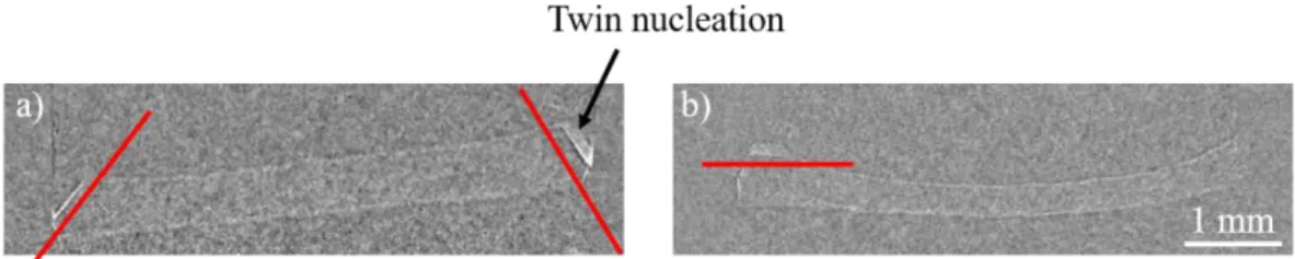
276
several diffraction spots related to specific lattice planes. The use of a polychromatic beam allows
277
collecting multiple spots in a single exposure that corresponds to different crystallographic planes
278
{hkl} of the same grain.
279
The transmission mode is used i.e. the incident beam is transmitted through the sample and the
280
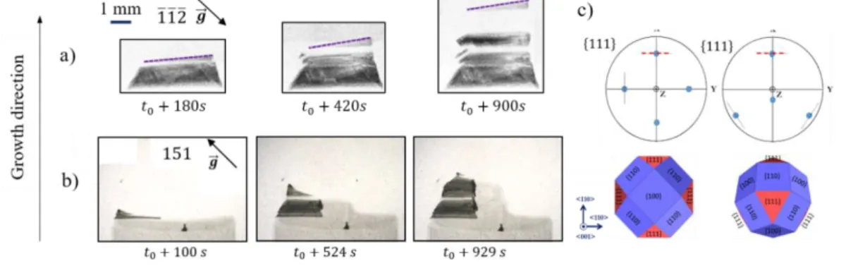
diffracted beams expose a detector that is placed after the sample. Transmission mode is the only
281
possible one in our experiments as the sample is installed inside the vacuum chamber containing the
282
furnace. The use of a polychromatic beam allows the collection of several spots originating from
283
multiple grains in a single exposure as well as several spots corresponding to the different
284
crystallographic planes of a single grain.
Each spot provides an image of the crystal generated by the beam diffracted by the {hkl} plane
286
family of a grain, called topograph [61]. These Bragg spots are then characterized by the hkl Miller
287
indices of the diffracting plane and by the projection of the diffraction vector 𝒈𝒈��⃗ (reciprocal lattice
288
vector), indicating the orientation of the spot with respect to the position of the direct beam. This
289
technique can obviously give information on the crystallographic orientations of the grains
290
considering the relative position of the diffraction spots, but its major output concerns the internal
291
structure of the individual spots as they contain information on misorientations, strain fields and by
292
extension on the presence of structural defects in general. Indeed, this is a powerful technique that
293
can be used for the visualization of defects (dislocations, twins, domain walls, inclusions, impurity
294
distribution) present in the crystal volume as it records their long range distortion fields and / or the
295
strain fields associated with a macroscopic crystal deformation. However, one drawback of the
296
technique is the complex analysis of the obtained images which are distorted images of the crystals.
297
The origin of the contrast observed in the images is briefly explained here, the reader is directed to
298
several references for more details [9, 59, 61-63].
299
Due to the small beam divergence of the incoming synchrotron X-ray beam and to its large size,
300
the whole width of our samples can be illuminated providing images exhibiting a minimum
301
geometrical deformation effect. In our case, the diffracting volume corresponds to the width of the
302
sample × the height of the field of view (generally 10 mm) × the thickness of the sample. It is worth
303
noting that contrarily to more classical diffraction configurations, a limited number of diffraction
304
spots can be collected during our experiments. This is due to both the distance between the sample
305
and the diffraction pattern detector and the detector size. Indeed, although distance minimisation is
306
always possible to some extent, some hard limits are imposed by the DS furnace vacuum chamber
307
needed to run solidification experiments. It explains why only a few diffraction spots are recorded
308
on the films when they are used to record the diffraction pattern.
309
A few mechanisms are responsible for the contrast and intensity on the X-ray topographs we
310
recorded. They are structure factor contrast, orientation contrast, and the so-called “direct image”
311
mechanism. All of them derive from diffraction theory and Bragg’s law as explained for example in
312
[64] and are evidenced in Figures 2 and 3.
313
314
Orientation contrast
315
316
A particularly clear illustration of the orientation contrast is given in the presence of twins
317
observed in our experiments (Figures 2 and 3) [46, 51].
318
319
320
Figure 2: X-ray diffraction images (topographs) recorded during solidification (applied temperature
321
gradient: 30 K/cm and cooling rate of -1 K/min applied on both heaters at t0) from a FZ seed, (a)
322
Crystallographic orientation of the seed, (b) Laue pattern recorded at the end of solidification showing
323
the diffraction spots in the field of view. Images of the (c) 1�11� and (d) 2�20 topographs recorded at
324
two instants during solidification.
Indeed, in the case of twinning during growth, the diffraction images are very different
326
depending on the diffraction spots as can be seen in Figure 2. A typical hatched aspect is observed
327
for the diffraction spots corresponding to {hkl} family planes as can be seen in Figure 2.b (e.g. α, β
328
and
χ
). The diffraction spotχ
(2�20) shows a diffraction spot corresponding to {hkl} family planes329
which are not common with twinned grains that developed on both right and left hand sides of the
330
sample (Figure 2.c). The complementary image corresponding to the twinned grains on the left
331
(Figure 2.b β) is found at another position of the diffraction pattern, whereas the diffraction spot α
332
(1�11�) includes the diffraction patterns of the common family planes of the central main grain and of
333
the twinned grains on the left (Figure 2.d). This is a particularly important element to be kept in mind
334
when analysing the topographs. Indeed, the observation of a single diffraction spot can be
335
misleading. This is one of the reasons why several diffraction spots must be analysed to be able to
336
conclude.
337
Orientation contrast can be also produced, for instance when the sample displays sub-grain
338
boundaries. For a monochromatic beam, the region corresponding to a {hkl} plane family is imaged
339
at a position given by the Bragg’s law. Regions of different crystallographic orientations are not seen
340
simultaneously on the diffraction image and appear as non-illuminated (white) zones. When a
341
polychromatic beam is used, the misoriented regions are all in diffraction position simultaneously,
342
but for different wavelengths. The images diffracted by neighbouring sub-grains can exhibit a
343
contrast associated with geometrical local superimpositions or separations of the diffracted beams on
344
the topographs, according to the dimensions of the misoriented zone and to the value of the
345
misorientation.
346
Crystalline defects such as precipitates, dislocations and impurities, act on the diffraction
347
process through their associated effective misorientation angle variation
𝛿𝛿𝜃𝜃
𝑚𝑚(𝑟𝑟⃗),
which can be348
approximated by Equation 2 [59, 63]:
349
𝛿𝛿𝜃𝜃
𝑚𝑚(𝑟𝑟⃗) =
𝛿𝛿𝑑𝑑
𝑑𝑑 (𝑟𝑟⃗)𝑡𝑡𝑡𝑡𝑛𝑛𝜃𝜃
𝐵𝐵± 𝛿𝛿𝜃𝜃(𝑟𝑟⃗)
(2)where θB is the Bragg angle, 𝛿𝛿𝑑𝑑
𝑑𝑑
(𝑟𝑟⃗)
is the local relative change of the lattice parameter and350
𝛿𝛿𝜃𝜃(𝑟𝑟⃗), the local change in crystallographic orientation. The double sign has to be chosen to take into
351
account the effect of the deformation on the Bragg angle (decrease or increase of its value). This
352
effective misorientation corresponds to the strain field generated by the defect, which is at the origin
353
of Bragg diffraction of components of the incident beam that do not participate to the diffraction for
354
the perfect crystal matrix [38, 62]. This is the “direct image” mechanism that leads, in the X-ray low
355
absorption case we are concerned with, to supplementary diffracted intensity associated to distorted
356
regions. Andrew Lang developed this technique and revealed dislocations in silicon in his pioneer
357
work [61]. The diffraction imaging technique was also used by Oriwol et al. [26] to study dislocations
358
and the formation of sub-grain boundaries ex situ in Si ingots. Indeed, diffraction imaging applied to
359
silicon crystals have proven to give unique insights into the evolution of dislocations [65, 66] and
360
cracks [67]. As can be understood from the above, one of the main advantages of diffraction imaging
361
is that it can reveal low scale structural defects like dislocations on wide field images encompassing
362
complete crystals as shown for example for diamonds by Burns et al. [62] and for Si [38, 53, 68].
363
364
An illustration is given in our work on Figure 3.c. In this topograph corresponding to the
365
11�1 diffraction spot and recorded during the solidification from a silicon FZ seed (orientation Figure
366
3.a), black contrasts revealing deformation of the crystal structure are present at several places.
367
Moreover, the deformation due to single dislocations can be clearly revealed in the seed and above
368
the seed-regrown interface.
370
Figure 3: X-ray diffraction imaging (topography) during solidification (applied temperature gradient:
371
30 K/cm and cooling rate of -1 K/min applied on both heaters) from a FZ seed, (a) crystallographic
372
orientation of the seed, (b) Laue pattern showing the diffraction spots recorded at the end of
373
solidification in the field of view, (c) topograph of the 11�1 diffraction spot during solidification.
374
Importantly, if the strain field created around a defect is related to particular crystallographic
375
orientations, it is not visible in all diffraction spot images (topographs). Indeed, if the displacement
376
vector is perpendicular to the diffraction vector, the defect is not visible on the topograph. This is the
377
case of dislocations whose image is extinct for the diffraction spots corresponding to diffraction
378
vectors perpendicular to the Burgers vectors as also seen in TEM investigations [69, 70]. On the one
379
hand, this means that the absence of a dislocation strain field on a single diffraction spot does not
380
mean that no dislocations are present. Depending on the dislocation character, at least two diffraction
381
spots with different diffraction vectors perpendicular to each other must be analysed before being
382
able to conclude on the presence or not of dislocations. On the other hand, extinction is a powerful
383
method to retrieve the Burgers vector direction as explained in details for example in [71].
384
2.1.5 Dynamic evolution
385
Another main originality of the experimental configuration we use is that several Laue patterns
386
or topographs are recorded during a solidification experiment [38, 46, 72]. Then, it is possible to
387
obtain sequences showing the evolution with time of the Laue pattern and of the topographs during
388
the development of the grains. Such sequences allow a better understanding of the competition
389
between the grains and of the occurrence of the twinning phenomenon. At the same time, the
390
dynamics of the formation and evolution of defects as dislocations is followed during growth. The
391
study of the growth of individual grains is then possible, along with the development of strain fields
392
produced in the crystal structure by the structural defects. The combination of both imaging
393
techniques and of the DS furnace provides complementary dynamic information about crystal
394
growth and competition and about the crystal structure deformation.
395
Up to 2018, both in situ and real time X-ray imaging techniques: X-ray radiography and Bragg
396
diffraction imaging (topography) were used alternately during growth. In this configuration, the
397
different diffraction spots are collected on photographic films positioned after the furnace regularly
398
during the experiment thanks to a specially designed device. X-ray diffracted beams are successively
399
recorded on X – ray sensitive films (AGFA Structurix D3-SC, 17.6×12.5 cm2) positioned at a distance
400
about 300 mm from the sample. The exposure time used to record the diffraction patterns is usually
401
of 0.5 s. In this configuration, radiographs and topographs are thus recorded alternately.
402
In 2018, we implemented together with the ESRF ID19 team a solution to record simultaneously
403
radiographs and diffraction images (topographs). In this configuration, a scientific CMOS camera
404
lens-coupled to a LuAG scintillator (commercial Ce-doped Lu3Al5O12, Crytur company – Czech
405
Republic) is used to record the images of one of the diffraction spots (topograph). The camera has
406
2048 × 2048 pixels with a nominal pixel size of 6.5 µm2 and a dynamic range of 16 bit. It is coupled
407
with a ×1.5 optic to decrease the pixel size to 4.3 µm2. In this new configuration, images recorded
408
from both modes are fully synchronised. The image acquisition rate is of 2 frames per second in
409
experiments reported in [53] which is sufficient to follow the solidification front of the samples. The
choice of the diffraction vector of the recorded spots and the alignment of the camera with respect to
411
the sample face is an important aspect because it influences the appearance and the information that
412
can be revealed from the recorded topographs. Ideally a spot with a high intensity induced by the
413
crystal plane structure factor should be chosen to better reveal defects. A detailed description of the
414
equipment and imaging methods and configurations (alternate or simultaneous recording) can also
415
be found in our previous publications [50, 51, 53].
416
2.2 Ex situ complementary investigations
417
After the last melting – solidification cycle, the samples are cooled down to room temperature
418
and removed from the GaTSBI furnace. Ex situ electron backscatter diffraction (EBSD) measurements
419
are performed after mirror polishing down to 1 µm diamond paste using a FEG-SEM JEOL JSM 7001F
420
equipped with a HKL Nordlys camera with either a 7 µm or a 0.7 µm step size depending on the
421
studied area. In order to depict the three – dimensional orientation of the crystals in the sample,
422
inverse pole figure (IPF) orientation maps are generated with respect to the three space directions:
423
normal to the sample surface (z), transverse direction (y) and in the growth direction (x). Moreover,
424
the coincidence site lattice map (CSL) is reconstructed to evidence the grain boundaries with a special
425
character. In this paper, Σ3 <111> (red colour in the maps), Σ9 <110> (blue) and Σ27a <110> (yellow)
426
twin boundaries labelling refer to rotations around <h k l> axis that satisfy the misorientation ranges
427
given by the Brandon criterion, (60 ± 8.66)°, (38.94 ± 5)° and (31.58 ± 2.89)°, respectively. Additionally,
428
the grain orientation spread (GOS) map is extracted as well from the EBSD results. The GOS map is
429
constructed by calculating the difference between the orientation of each pixel in the grain and of the
430
grain average orientation to evidence the more distorted areas within a grain structure. A colour code
431
is used to depict the grains without deformation (perfect Si crystal appears in blue) and having an
432
average crystal structure deformation (red colour for the highest deformation).
433
3. Results and discussion
434
3.1.
{111}
facet growth and undercooling435
Theoretical models of the {111} facet growth laws exist [73, 74] and are related to the
436
undercooling at the level of the {111} facets. However, the orders of magnitude of the undercooling
437
values for the corresponding laws are very different, so that experimental validation is needed.
438
Moreover, directional solidification is widely used for the fabrication of multi-crystalline ingots so
439
that the knowledge of {111} facet dynamics needs to be known during DS. Moreover, it constitutes a
440
critical building block to develop predictive and quantitative models [75-77]. Moreover, the presence
441
of {111} facets at the solid-liquid interface leads to the occurrence of twinning ultimately competing
442
with the central grain growing from the seed as will be discussed in the following. It is thus essential
443
to understand their formation mechanism and the undercooling at their level which gives conditions
444
for twin nucleation. Our main objective has thus been to determine the contribution of the
445
undercooling of the {111} facets at the solid-liquid interface during Si directional solidification. {111}
446
facet growth laws are derived and then compared with theoretical growth models reported in the
447
literature.
448
At the level of the solid-liquid interface, {111} facets appear at the sample edges and in grain
449
boundary grooves. Grain boundary grooves are formed due to the encounter between a grain
450
boundary and the solid-liquid interface [78]. From the theory [79], grain boundary grooves can be
451
either facetted/facetted, facetted/rough or rough/rough depending on the crystallographic
452
orientation of the adjacent grains. Experimentally, we are able to characterize facetted/rough and
453
facetted/facetted grain boundary grooves [48, 80] with a large prevalence for the facetted/facetted
454
configuration. However, conclusions concerning the predominance of one or the other grain
455
boundary groove type cannot be drawn from these observations as rough/rough grain boundary
456
grooves are expected to correspond to lower undercoolings compared to facetted/facetted ones and
457
thus to smaller depth that can then fall below the spatial resolution used in these experiments.
Whatever conditions, facets observed in our experiments are always {111} facets as foreseen in
459
silicon [81]. It was checked by determining the crystallographic orientation of the grains and their
460
relative {111} facet orientation. In order to determine {111} facet growth laws, the grain boundary
461
grooves observed at the solid-liquid interface (e.g. in Figures 1 & 4) have been geometrically
462
characterized by their angle and depth in the case of an ideal facetted/facetted groove [82]. The
463
geometrical parameters of the grain boundary grooves can be measured directly on the radiography
464
images collected during solidification (Figures 1 & 4). The kinetic parameters, growth velocity of the
465
interface and normal growth velocity of the groove facets are also measured thanks to the
time-466
resolved observation of the solid-liquid interface evolution.
467
When comparing the growth rate of the global solid-liquid interface to the {111} facet growth
468
rates, it appears first that the growth rates of the {111} facets both inside the grooves and at the edges
469
are smaller than the one of the global solid-liquid interface. This is expected because of the slower
470
kinetics of the {111} planes compared to the other crystallographic orientations so that they are
471
lagging behind other growing orientations and generally behind the global solid-liquid interface [47].
472
A major consequence is that the undercooling is higher in the groove and at the level of the edge
473
facets compared to the one at the level of the global solid-liquid interface. This favors nucleation
474
events inside grooves and at the edge facets that are indeed often observed in real time during our
475
experiments.
476
477
478
Figure 4: X-ray radiography images recorded during solidification, applied temperature gradient: 30
479
K/cm and cooling rate = -1 K/min applied on both heaters. Typical facetted / facetted grain boundary
480
groove revealed by division by successive images.
481
The dynamics of a facetted / facetted groove during solidification can be seen for example in
482
Figure 4. Both facets grow at the same growth rate as can be concluded from the constant angle and
483
orientation of the groove. This conclusion is also sustained by the X-ray radiography images contrast
484
(Figure 4.c). The white areas on the facets evidence the new grown solid between two successive
485
images because of the image processing performed as explained in the experimental section. These
486
white regions have the same thickness on both facets which indicates that both facets grow at the
487
same rate. This is observed in all studied cases for facetted/facetted grain boundary grooves.
488
The maximum thermal undercooling inside a grain boundary groove can be calculated knowing
489
the local temperature gradient and the maximum grain boundary groove depth. Details of the
490
calculations can be found in [48]. The measured maximum undercooling has been thus calculated
491
inside grain boundary grooves for several experiments with seeds oriented along <100>, <111> and
492
<110> directions. In all cases, the maximum undercooling inside the grain boundary groove is found
493
to be always lower than 1 K ranging from 1 x 10⁻¹ to 4 x 10⁻¹ K and adds to the solid-liquid interface
494
undercooling [47]. Eventually, the mean facet velocity evolution as a function of the additional
495
undercooling inside the grain boundary grooves can be obtained.
496
Moreover, {111} facets are also observed at the level of the solid-liquid interface at the sample
497
edges as can be seen in Figures 1.c and 5. The same procedure is applied to the {111} facets at the
498
edges of the samples except that there is only one facet to consider in this case.
500
Figure 5: X-ray radiography images of the solid-liquid interface during growth with {111} facets at
501
both edges of the sample for the experiments: (a) same experiment as in Figures 2 and 6.a, (b) same
502
experiment as in Figure 6.c. Red lines indicate the traces of {111} planes.
503
At the level of the edge facets, the measured maximum undercooling is again always lower than
504
1 K. However, higher values (ranging from 2 x 10⁻¹ to 8 x 10⁻¹ K) compared to the undercooling inside
505
grain boundary grooves are measured at the edges. This result is significant because the same
506
evolution is obtained for several samples and for both grooves at the edges independently from
507
possible sample particularities. The higher undercooling measured at the level of the edge {111} facets
508
has a significant impact on the grain structure obtained at the end of solidification as it increases the
509
nucleation probability during growth at the level of the edge facets. This is clearly confirmed by the
510
grain structure obtained in the samples at the end of the experiments for which twin nucleation is
511
frequent at the far edges of the facets (Figure 6). This major contribution of twins nucleating on edge
512
{111} facets to grain competition and final grain structure was previously reported [7, 38] and was
513
observed repeatedly in our experiments.
514
The undercooling inside the grain boundary grooves and at the level of edge facets is always
515
lower than 1 K relatively to the global solid-liquid interface which is far smaller than the undercooling
516
values predicted by the bi-dimensional laws (several K) for the growth rates measured during these
517
experiments. As a consequence, bi-dimensional nucleation growth mechanism [73] can be excluded.
518
The experimental results concerning {111} facets kinetics in our experiments can only be compared
519
favourably to the theoretical law corresponding to a growth mechanism eased by the presence of
520
dislocations proposed by Voronkov [74]. This is in agreement with the fact that dislocations are
521
expected to be easily generated during silicon growth and found emerging at the level of facets as
522
shown for example in [38, 83] and as can be seen in Figure 3.
523
3.2 Twinning during solidification:
524
As discussed in the introduction, the crystalline quality of the ingot and the grain boundary
525
types, in particular the twin boundary characteristics, can have a significant impact on the
526
photoelectric properties [22, 27]. It has been shown that perfect symmetric Σ3 twins have no major
527
impact on the photovoltaic performance. However, the repetition of twinning has important
528
consequences for the final grain structure and distribution of crystallographic orientations [31].
529
Indeed, the importance of twinning in the development of the grain structure has been highlighted
530
for different solidification processes ranging from directional solidification [84] to ribbon growth [33,
531
85-86]. In the past few years, we studied rather extensively twin formation, growth and its
532
consequences on the final grain structure and defect formation in general [38, 46, 48, 49, 51, 53, 87].
533
3.2.1 Twin nucleation
534
Four typical final grain structures of samples solidified from a seed in the GaTSBI DS furnace
535
are shown in Figure 6. The coincidence site lattice maps (middle line in Figure 6) are shown in order
536
to reveal the grain boundary character and in particular the twin boundaries. These samples are
537
solidified from float-zone (FZ) monocrystalline seeds (Figures 6.a and b) and from Czochralski (Cz)
538
seeds (Figures 6.c and d) after partial melting of the seed. The samples are solidified from seeds with
539
different crystallographic orientations in the growth direction (Figure 6 bottom line). In all cases, side
540
twins develop at the edges from {111} facets and compete with the main central grain issued from the
541
seed, as it was also observed by Trempa et al. [7] in a systematic study. The fact that the behavior of
FZ and Cz seeds is comparable suggests that the presence of oxygen (typically: 0.5 – 1 x 10¹⁸ at/cm3 in
543
Cz ingots compared to < 1015 at/cm3 in FZ ingots) is not a predominant factor for the twin nucleation.
544
545
Figure 6: EBSD measurements revealing the grain structure and twin boundaries after growth and
546
cooling down in samples grown from monocrystalline seeds. Applied temperature gradient: 30 K/cm
547
and cooling rate applied on both heaters (a) -1 K/min (same experiment as in Figures 2, 8.a-b and 9),
548
(b) -1 K/min, (c) -0.2 K/min (same experiment as in Figures 7.b, 8.c-e), (d) applied temperature
549
gradient: 20 K/cm and cooling rate: -0.2 K/min (same experiment as in Figure 7.a). Top: Inverse Pole
550
Figure (IPF) map along the growth direction. Middle: CSL (Coincidence Site Lattice) map. Bottom:
551
Seed orientation and {111} planes.
552
Figures 5.a and 5.b correspond to a snapshot at one instant during solidification showing the
553
solid-liquid interface of samples in Figures 6.a and 6.c, respectively. The in situ X-ray radiography
554
images (Figure 5) reveals that the solid-liquid interface is smooth during growth under these
555
conditions for both Cz (Figure 5.a) and FZ (Figure 5.b) seeds. No destabilization of the interface can
556
be observed in all cases when Cz or FZ seeds are used. Interface destabilization has only been
557
observed in the presence of Cu impurities as reported in [54].
558
Despite the global smooth interface, {111} facets can be clearly seen on the X-ray radiography
559
images at the edges of the sample (Figure 5). It was verified that they correspond to the projection of
560
{111} facets by determining the corresponding pole figures using the measurements performed by
561
EBSD. The {111} facet orientation is highlighted by the red lines on Figure 5. Twin nucleation takes
562
place regularly on these {111} facets as can be seen for example on Figures 5.a (right) and 5.b (left). A
563
video of radiograph images showing the dynamic evolution of the solid-liquid interface during the
564
experiment corresponding to Figures 2, 5.a and 6.a is provided as supplementary material. It
565
evidences, twin nucleation at the {111} edge facets and the formation of grain boundary grooves at
566
the solid-liquid interface due to the subsequent grain competition.
567
Diffraction spot images collected at different times during the solidification of the two samples
568
(corresponding to the experiments and grain structure in Figures 6.c and d) are shown in Figure 7.
569
The diffraction spots in Figure 7.a display the twinning zone at the right side of the sample in Figure
570
6.d, whereas the diffraction spots in Figure 7.b display the twinning zone at the left side of the sample
571
in Figure 6.c. The purple dotted line is added in Figure 7.a to indicate the corresponding solid-liquid
572
interface shape as observed in the radiographs. It is worth reminding that diffraction imaging shows
573
only the crystalline solid areas. The observation of the upper part of the diffraction spots shows that
574
the twin nucleation occurs at the edges of the samples at the solid-liquid-vacuum-crucible phase line
575
as also seen in the radiographs (Figure 5 and supplementary material). A sudden increase of the solid
576
height at the solid-liquid interface is observed at the instant of each new twin nucleation on the
time-577
resolved radiography images. From these height differences a value of the nucleation undercooling
578
has been estimated and it ranges from 0.1 K to 0.5 K for the experiment corresponding to Figures 5.b,
6.c and 7.b, which is also consistent with the results reported in section 3.1. These measurements
580
confirm that the undercooling measured in grain boundary grooves and at the edges are sufficient
581
for twin nucleation on the {111} facets.
582
A 3D model was proposed by Jhang et al. [88] to determine the nucleation probability at the level
583
of {111} facets. This model was specifically applied to several of our experimental cases. The twin
584
grain nucleation probability was found to be higher when there is a contact between the {111} facet
585
and crucible walls. This is generally the case in our thin sample configuration. Additionally, the
586
authors showed that the attachment energy and the contact area with crucible walls are the key
587
factors for the heterogeneous nucleation of twins. Low attachment energy and lower contact area
588
concur to the highest twining probability on the {111} facets. When applied to our experimental case,
589
it is found that twin grain nucleation probability is higher at the sample edge {111} facets compared
590
to the ones situated in grain boundary grooves, where the attachment energy and the bottom contact
591
area of the twin nucleus tend to be lower. This is in agreement with the experimental observations.
592
593
Figure 7: Image sequence of diffraction spot images – topographs corresponding to twinning zones
594
(a) twinning zone corresponding to the right side of sample Figure 5.d. The purple dotted line
595
correspond to the solid-liquid interface, (b) twinning zone corresponding to the left side of sample
596
Figures 5.c and 6.b, (c) stereographic projections of the {111} planes of the seed (left) and the first
597
twin (right) with both horizontal projections for the experiment in (b) and the corresponding 3D
598
representation of the plane arrangements (below).
599
Moreover, the twin growth rate at the nucleation instant (about 15 µm/s) exceeds the one of the
600
global solid-liquid interface (2 µm/s). The consequence is that the twin grains that nucleate on the
601
edges grow vertically very fast and in advance compared to the global solid-liquid interface inducing
602
the triangular images recorded during solidification on the topographs. Such a triangular shape of
603
the twins growing at the solid-liquid interface has been repeatedly observed in our experiments
604
during solidification. When the crystal arrives at the liquidus isotherm position, stabilization of the
605
growth rate is observed until the global solid-liquid interface arrives at the liquidus. As a subsequent
606
step, a growth rate plateau is measured, after which the next twin nucleation can take place [38]. The
607
nucleation of the twin and growth upwards along the directional solidification direction goes along
608
with the propagation of the twin grains towards the center as revealed by the topographs (Figure 7).
609
A main result of our work is that only Σ3 type twinned grains nucleate during growth. This
610
conclusion can only be drawn because we are able to monitor the growth in situ with X-ray imaging.
611
3.2.2 Successive Twinning
612
The successive twinning zones are immediately identifiable on ingots after solidification. It is
613
evidenced on both the grain structure EBSD maps (Figure 6, upper line) and diffraction images for
614
example on Figures 2, 3 and 7. The successive twinning zone is observable by the alternation of two
615
crystallographic orientations (Figure 6) on the EBSD maps and by the striped/hatched aspect of the
616
topographs (Figures 2, 3 and 7). Only two crystallographic orientations alternate and they share a
617
common {111} plane. The fact that crystallographic orientations are found successively can be
618
explained by the orientation of both seed and first twin grain. The stereographic projection of {111}
619
planes of both the seed and first twin grain (green and pink color in Figure 5.c, respectively)