Science Arts & Métiers (SAM)
is an open access repository that collects the work of Arts et Métiers Institute of
Technology researchers and makes it freely available over the web where possible.
This is an author-deposited version published in: https://sam.ensam.eu Handle ID: .http://hdl.handle.net/10985/9703
To cite this version :
Khadidja RAHMOUN, Alain IOST, Vincent KERYVIN, Gildas GUILLEMOT, Jean-Christophe SANGLEBOEUF, Mohamed GUENDOUZ, Lazhar HAJI - Vickers Microhardness of Oxidized and Nonoxidized Porous Silicon - In: Dielectric Materials for Photovoltaic Systems (NAWDMPV), 2014 North African Workshop on, Algérie, 2014-10-26 - Dielectric Materials for Photovoltaic Systems (NAWDMPV), 2014 North African Workshop on - 2015
Any correspondence concerning this service should be sent to the repository Administrator : [email protected]
Science Arts & Métiers (SAM)
is an open access repository that collects the work of Arts et Métiers ParisTech
researchers and makes it freely available over the web where possible.
This is an author-deposited version published in: http://sam.ensam.eu Handle ID: .http://hdl.handle.net/null
To cite this version :
Khadja RAHMOUN, Alain IOST, Vincent KERYVIN, Gildas GUILLEMOT, Jean-Christophe SANGLEBOEUF, Mohamed GUENDOUZ, Lazhar HAJI - Vickers Microhardness of Oxidized and Nonoxidized Porous Silicon - In: Dielectric Materials for Photovoltaic Systems (NAWDMPV), 2014 North African Workshop on, Algérie, 2014-10-26 - Dielectric Materials for Photovoltaic Systems (NAWDMPV), 2014 North African Workshop on - 2015
Any correspondence concerning this service should be sent to the repository Administrator : [email protected]
Vickers Microhardness of Oxidized and Nonoxidized
Porous Silicon
K. Rahmoun
1, A. Iost
2, V. Keryvin
3, 4, G. Guillemot
2, J. C. Sangleboeuf
3,M. Guendouz
5, L.Haji
51Unité de Recherche Matériaux et Energies Renouvelables URMER,
University of Tlemcen, BP 119, Tlemcen 13000, ALGERIE
2CNRS UMR 8517, Equipe Caractérisation et Propriétés de la Périsurface,
Arts et Métiers ParisTech, MSMP, 8 Boulevard Louis XIV, 59046 Lille cedex, FRANCE
3 Département Mécanique et Verres, IPR, UMR 6251 - CNRS/Université de Rennes 1,
Bât. 10B, Campus de Beaulieu, 35042 Rennes cedex, France
4Universite´ de Bretagne-Sud, EA 4250, LIMATB, F-56100 Lorient, France
5Laboratoire Foton, CNRS-UMR FOTON 6082, Université de Rennes 1, ENSSAT, 6
Rue de Kérampont, BP 80518, 22305 Lannion Cedex, France 1 [email protected] 2 [email protected] 2 [email protected] 3,4 [email protected] 3 [email protected] 5 [email protected] 5 [email protected]
Abstract
—
In this work we present our recent investigation on characterizing mechanical properties of porous silicon (PS) by using instrumented micro-indentation. Hardness and elastic modulus for oxidized and nonoxidized PS were measured. Experimental results revealed that hardness and elastic modulus are significantly lower than that of silicon substrate and decrease with increasing porosities. After oxidation an increase of the hardness and elastic modulus were observed. The task of stabilization of PS mechanical parameters can be solved with the help of oxidation.Keywords
—
Vickers indentation, Microhardness, Elastic modulus, Porous silicon, OxidationI. INTRODUCTION
The evolution of micro-electronics took place thanks to the development of the semi conductors among which one finds silicon. Silicon quickly was imposed like material impossible to circumvent: it offers many advantages (low costs, good controls), which lead to its use in 95% of modern micro-electronics. Since the discovery of the intense photoluminescence of porous silicon, many studies developed in the world for its use in varied applications. In particular, porous silicon has been investigated extensively as a possible candidate for developing light emitting, photonics, optoelectronics [1-4] and biophotonic [5] devices.
Porous silicon, with its crystalline nanoporous structure, is presented in the form of a material original, able to emit light, but able also to be used as matrix of reception with many liquid materials, amorphous solids or crystalline lens,… a large variety of devices is thus possible to be realized. All
these ambitions are of course closely related to problems of structural behavior. The behavior of porous silicon changes according to its conditions of preparation related to its use in various fields.
Freshly made PS is known to be unstable, showing considerable ageing effects that limit its use in practical applications. Porous silicon (PS) layers with high porosity are of great interest; unfortunately, this material was found to be mechanically unstable during drying. Capillary forces have been invoked to explain such cracking [6].
One way to stabilize the PS layers is by thermal oxidation. The common explanation for the improved stability in oxidized PS is a replacement of the hydrogen coverage of the pore walls by more stable layers of silicon dioxide [7]. The study of the mechanical properties of PS is thus very important in order to better apprehend the mechanical resistance of the devices.
In this work we present our recent investigation on characterizing mechanical properties of the (PS) layers. The Hardness and elastic modulus for oxidized and nonoxidized PS were measured.
II. EXPERIMENTATION
A. Sample preparation
Porous silicon layers were obtained by anodization of a (100) oriented monocristalline p+ silicon wafer with (4- 6 mΩcm) resistivity in a hydrofluoric acid/ethanol electrolyte. The electrolyte was composed of HF (50%): H2O: ethanol (2:1:2).
Anodization was performed at room temperature in the dark and under galvanostatic conditions. The applied current
density was ranging from 50 to100 mAcm-2 in order to obtain
various porosities. The porosity of the obtained layers was measured from gravimetric measurement [8].
After etching, the samples were cleaned with de-ionized water, dried and stored in ambient air at room temperature.
Some of as prepared samples were oxidized in order to obtain porous silica At first, samples were pre-oxidized at 300°C for one hour following by an oxidation step at 900°C in wet O2 for one hour . Their morphology was studied by
Scanning Electron Microscopy (SEM).
B. Microindentation tests
The microhardness measurements were performed with a micro-indenter Fischerscope H100 XYp (maximum load of 1 N, load resolution of 0.02 mN, depth resolution of 2 nm) at ambient laboratory conditions. Indentation consists in continuously applying a load to a specimen via a sharp Vickers pyramid indenter and to continuously monitor the depth of penetration in the sample. This leads to the following expression for hardness [9]:
)
/
(
8544
.
1
P
d
2HV
=
L (1)Where d (mm) is the mean diagonal length of the diamond shaped indent and PL is the applied load.
We also measured the Martens hardness, HM by the following equation: 2 max
43
.
26
h
P
HM
=
(2) Whereh
is the indentation depth andP
max the maximumapplied load.
The hardness is defined as the indentation load divided by the projected contact area and the elastic modulus can be calculated based on the relationship developed by Oliver et Pharr [10]. The so-called reduced modulus (Er) was derived
by: r
E
A
S
π
β
2
=
(3) Where A is the projected contact area of the indenter with the sample surface,β =1.012
for Vickers’ indenter, S the contact stiffness and Er is the reduced modulus which is calculatedfrom: i i r
E
E
E
2 21
1
1
=
−
ν
+
−
ν
(4)E and ν are the elastic modulus and Poisson’s ratio of the
sample and Ei (1140 GPa) and
ν
i (0.07) are the elasticproperties of the diamond indenter, respectively.
III. RESULTS AND DISCUSSION
The surface of the PS samples was observed under a Scanning Electron Microscopy (SEM), a JEOL JMS 6500F and a HITACHI 2460N with variable pressure.
For the completely oxidized samples one supposes that the matrix is entirely made up of oxide silicon (SiO2).
Micrographies not having been taken directly after formation of porous film, part of the phase stamps was oxidized with the ambient air.
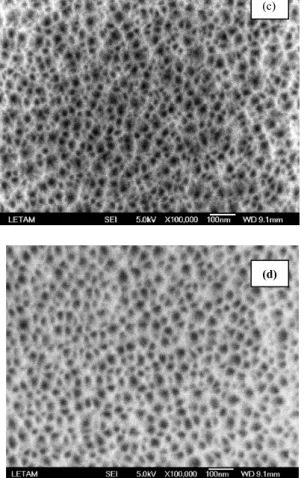
The etching direction is from top to bottom, PS has been classified depending on the size of micropores as microporous (< 5 nm), mesoporous (5-50 nm) and macroporous (> 50nm) [8]. Figure 1 shows SEM pictures of the top surface of the 60% porosity p+-type PS layer (a) and à 80% porosity (b). These micrographs allowed the size and density of pores to be estimated [11]. It could be seen that the porous layer was composed of a pore network separate by silicon crystallites and pore size varied from 7 to 30 nm revealed mesoporous layers. In figure 2 we can see that after oxidation the pore shape is conserved in spite of size reduction. It shows the SEM pictures of the top surface of the 60% (a) and a 80% (b) porosity of the p+-type oxidized porous silicon layer.
Fig.1 SEM micrographs of the top surface of 60% (a) and 80% (b) the initial porosities, 5 μm thick PS film
.
(a)
A cross section in figure 3 shows an anisotropic microstructure: the pores are perpendicular to the surface of the silicon substrate and were considered as cylindrical with numerous side branches which have almost the same size as the pore mean diameter. The thickness of the sample can be estimated to 5µm.
Fig.2 SEM micrographs of the top surface of 60% (c) and 80% (d) initial porosities, 5 μm thick oxidized PS film
Fig.3 SEM micrograph of the cross section of the 5 μm thick PS film. The porosity was initially about 60%.
Mechanical properties of nonoxidized (NO) and oxidized (O) porous silicon layers 5 μm-thick (t) for an applied load of
F=500 nm/20s according to the indentation dept h with h<t/10
for ten indentation per sample were summarized in table 1.
A. Elastic modulus
The influence of the substrate is important at penetration depth h > 10% of the film thickness [12]. Elastic modulus changes with the relative penetration depth, indicating that the indenter deforms not only the film but also the substrate, and the substrate influence is more pronounced at higher loads. Fig. 4 shows the influence of the indentation load on the measured elastic moduli for ten indentations.
Reduced modulus of PS5NO was found to be between 15 and 45.50 GPa. The Elastic modulus tends to increase with increasing applied load exhibiting significant dependence on the indentation load. The measures revealed that as the indentation depth (511 nm, 2840 nm and 6728 nm) increases the elastic modulus increases gradually.
0 800 1000 15 20 25 30 35 40 45 50 Elast ic m odul us ( G P a) Indentation load(mN)
Fig. 4Elastic modulus as a function of indentation load for PS5NO of 80% porosity.
As shown in table 1, all the results confirm a decrease of the elastic properties in function of the porosity for both oxidized and nonoxidized PS layers; 24.68 GPa and 14.98 GPa for a 60% and 80% porosity, 37.56 GPa and 21.39 GPa for oxidized PS. The measured elastic modulus is found to be drastically dependent on the porosity and is lower than those of the Si substrate where the value measured with a maximum load of 1mN is 130.35 GPa ±12.4 %.
For oxidized porous silicon some part of the Si “skeleton’’ x has been oxidized and transformed into SiO2, occupying
volume 2.27x [13] (Bonding of silicon with oxygen produces a 2.27 time volume rise of the solid skeleton). Thus, Si volumetric fraction after oxidation will be f- x, and that of pores will be
P
=
1
−
(
f
−
x
)
−
2
.
27
x
, f is considered as the silicon volumetric fraction. For the PS nonoxidizedin
P
f
= 1
−
with Pin the initial porosity before oxidation. (c)TABLE I
Hardness, elastic modulus, and initial porosity for porous silicon . Sample Pin (%) HM (GPa) HIT (GPa) HV (Kgfmm-2) E/(1-ν 2) (GPa) PS1NO 60 1025.95±2.91 1573.38±4.27 148.68±4.27 24.68±1.23 PS2O 60 2150.99±2.08 4510.19±2.35 426.21±2.35 37.56±2.04 PS5NO 80 448.76±5.13 590.66±6.06 55.82±6.06 14.98±3.49 PS6O 80 913.39±2.19 1404.98±2.76 132.77±2.76 21.39±1.03
It is then clear that elastic modulus for oxidized PS was found to be greater than that of nonoxidized porous silicon. PS is used as a host matrix by infiltrating pores with solids and liquids, as semiconductors, polymers or several organic molecules. S.P. Duttagupta [14] studied microhardness of PS films of different porosities, by infiltrating the pores with polymers. An increase in the hardness was observed without affecting photoluminescence (PL) intensity.
In our case, pores are filled with SiO2 then, the task of
stabilization of PS mechanical parameters can be solved thanks to the oxidation step.
B. Hardness
Fig. 5 shows the influence of the indentation depth on the hardness of oxidized and nonoxidized PS film at higher load (1000 mN) to confirm the ISE.
The measured hardness increases with increasing indentation depth. The “u-shaped” profile observed here is typically observed in the mechanical properties of low-dielectric-constant films [15, 16]. The First region is due probably at a cap layer formed on the surface by the natural oxidation; the second region shows the effect of the Si substrate. Clearly, the Hardness decreases with increasing porosity and an improvement of the mechanical properties is allowed with the oxidation as shown in figure 5. The measured hardness is found to be drastically dependent on the porosity and is lower than those of the Si substrate where the value measured with a maximum load of 1mN is 1374.44 Kgfmm -2 ± 25.13% (13.74 GPa). 0,0 0,5 1,0 1,5 2,0 2,5 3,0 3,5 4,0 1300 1400 1500 1600 2100 2200 2300 2400 2500 2600 2700 P=60% PS1NO PS2O Ha rd ne ss H M (Nm m -2 ) h(um) 0 1 2 3 4 5 6 450 500 550 600 650 700 750 800 850 900 950 1000 1050 1100 P=80% PS5NO PS6O H ar d ne ss H M (Nm m -2) h(um)
Fig. 5 Hardness HM of oxidized and nonoxidized PS film at higher load (1000 mN)
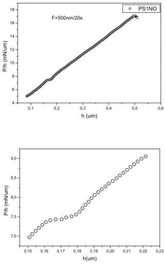
Figure 6 shows the load / indentation depth (P/h) versus indentation depth (h) curves. The relation between P/h and h should be linear if the material is homogeneous with a constant slop [17, 18]. However, this linear relation will change if the material under indentation changes.
0,1 0,2 0,3 0,4 0,5 0,6 4 6 8 10 12 14 16 18 F=500nm/20s PS1NO P /h (m N/ um ) h (um) 0,15 0,16 0,17 0,18 0,19 0,20 0,21 0,22 0,23 7,0 7,5 8,0 8,5 9,0 P /h (mN /um) h(um)
Fig. 6 Load indentation depth (P/h) versus indentation depth of the 5μm thick PS1NO film
In Figure 6 there is a sudden transition of the slop around the change indicating the presence of the contamination with natural oxidation.
Figure 7 reveals a good linearity especially for the oxidized porous film at high load for the square of the load
P
[18] versus indentation depth curves. This result proves that the indentation load / size effect on hardness exists in the applied load range [17]. 0 1 2 3 4 5 0 5 10 15 20 25 30 35 F=1000mN/20s PS1NO P 1/ 2 (m N 1/ 2 ) h(um) 0,0 0,5 1,0 1,5 2,0 2,5 3,0 3,5 4,0 0 50 100 150 200 250 300 F=1000mN/20s PS2O P 1/ 2 (m N /u m ) h (um)Fig.7 Load indentation depth
P
versus indentation depth of the 5μm thick PS1NO and PS2O filmIV. CONCLUSIONS
The mechanical properties of porous silicon of 60% and 80% initial porosities, 5 μm thick oxidized and nonoxidized films are measured.
The porosity plays an important role in affecting the mechanical properties as well as the surface morphology of PS films.
Hardness and elastic modulus changes with the relative penetration depth .
The measured hardness is found to be drastically dependent on the porosity and is lower than those of the nonporous Si. Elastic modulus and hardness for oxidized PS were found to be greater than that of nonoxidized porous silicon.
The linearity of P/h versus h can be used as an indication of characterization of the mechanical deformation of the porous film. The task of stabilization of PS mechanical parameters can be solved thanks to the oxidation.
ACKNOWLEDGMENT
One of the authors (K.R) wants to thank Pr. T. Rouxel for her proposal of a research stay at Laboratory LARMAUR, University of Rennes 1. The authors whish to thank J. Le
Lannic (CMEBA, University of Rennes 1), Pr A. Ougazzadene (LMOPS, University of Metz) and Dr N. Maloufi (LETAM, University of Metz ) for HR SEM or SEM.
REFERENCES
[1] N. Koshida, N. Matsumoto, Fabrication and quantum properties of nanostructured silicon, Mater. Sci. Eng. R 40 (2003)169-205
[2] L.T. Canham, T.I. Cox, A. Loni and A.J. Simons, Progress towards silicon optoelectronics using porous silicon technology, Appl. Surf. Sci.102 (1996) 436.
[3] A. Loni, L.T. Canham, M.G. Berger, R. Arens-Fisher, H. Munder, H. Luth, H.F. Arrand, T.M. Benson, Porous silicon multilayer optical waveguides, Thin solid Films, 276, (1996) p 143.
[4] N.M. Kalkhoram, Porous silicon- based optoelectronic devices: processing and characterisation, Mater. Res. Soc. Symp. Proc. 283 (1993) 365.
[5] S. Ben-Tabou de Leon, A. Sa’ar, R. Oren, M. E. Spira and S. Yitzchaik, Neurons culturing and biophotonic sensing using porous silicon, Appl. Phys. Lett. 84, (2004), 4361
[6] O. Belmont, D. Bellet, Y. Brechet, Study of the cracking of highly porous p+ type silicon during drying, J. Appl. Phys. 79 (1996) 7586 [7] V. Mulloni, L. Pavesi, Electrochemically oxidised porous silicon
microcavities, Material Science and Engineering : B ,69-70 (2000) 59-65
[8] O. Bisi, Stefano Ossicini, L. Pavesi, Porous silicon: a quantum sponge structure for silicon based optoelectronics, Surface Science Reports 38 (2000) 1-126
[9] D. Chicot, J. Lesage, Absolute hardness of films and coatings , Thin Solid Films, 254 (1995) 123
[10] W.C. Oliver, G.M. Pharr, An important technique for determining hardness and elastic modulus using load and displacement sensing indentation experiments, J. Mat. Res. 7 (1992) 1564-1583.
[11] P. Pirasteh, J. Charrier, A. Soltani, S. Haesaert, L. Haji, C. Godon, N. Errien, The effect of oxidation on physical properties of porous silicon layers for optical applications, App. Surf. Sci. 253 (2006) 1999-2002 [12] W.C. Oliver, R. Hutchings, J.B. Pethica, Measurement of hardness at
indentation depths as low as 20 nanometres, ASTM STP 669, 90 (1986) [13] E.V. Astrova, V. A.Tolmachev, Effective refractive index and
composition of oxidized porous silicon films, Material Science and Engineering: B69-70, (2000) 142-148.
[14] S.P. Duttagupta, X.L. Chen, S.A. Jenekhe, P.M. Fauchet, Microhardness of porous silicon films and composites, Solid State communications, Vol.101, No.1, (1997) 33-37.
[15] L. Chen, K. Zeng, Comparison of mechanical properties of porous and non-porous low-kdielectric films, Microelectronic. Eng. 71 (2004) 221 [16] M. Fujikane, S. Nagao, X.W. Liu, D. Chrobak, A. Lehto, S. Yamanaka,
R. Nowak, Evaluation of carbon-doped low-k multilayer structure by nanoindentation, Journal of Alloys and Compounds 480 (2008), 293-297
[17] Byung-Koog Jang, Influence of low indentation load on Young’s modulus and hardness of 4% Y2O3-ZrO2 by nanoindentation, J. Alloys Compounds, 426 (2006) 312-315
[18] K. Rahmoun, A. Iost, V. Keryvin, G. Guillemot, N.E. Chabane Sari, A multilayer model for describing hardness variations of aged porous silicon low-dielectric-constant thin films, Thin Solid Films, Volume 518, Issue 1, 2 November 2009, Pages 213-221