SHERBROOKE
Faculte de genie
Departement de genie electrique
SIMULATION AND DESIGN METHODOLOGY FOR HYBRID SET-CMOS LOGIC AT ROOM TEMPERATURE OPERATION
SIMULATION ET METHODOLOGIE DE CONCEPTION DE CIRCUITS LOGIQUES HYBRIDES SET-CMOS OPERANTS
A
TEMPERATURE AMBIANTEJury: Dr. Dominique Drouin Dr. Jacques Beauvais Dr. Rejean Fountain Dr. Serge Charlebois Dr. Chunhong Chen These de doctorat Speciality : genie electrique
Rutu PAREKH
Published Heritage Branch Direction du Patrimoine de I'edition 395 Wellington Street Ottawa ON K1A0N4 Canada 395, rue Wellington Ottawa ON K1A 0N4 Canada
Your file Votre reference ISBN: 978-0-494-89687-7 Our file Notre reference ISBN: 978-0-494-89687-7
NOTICE:
The author has granted a non
exclusive license allowing Library and Archives Canada to reproduce, publish, archive, preserve, conserve, communicate to the public by
telecommunication or on the Internet, loan, distrbute and sell theses
worldwide, for commercial or non commercial purposes, in microform, paper, electronic and/or any other formats.
AVIS:
L'auteur a accorde une licence non exclusive permettant a la Bibliotheque et Archives Canada de reproduire, publier, archiver, sauvegarder, conserver, transmettre au public par telecommunication ou par I'lnternet, preter, distribuer et vendre des theses partout dans le monde, a des fins commerciales ou autres, sur support microforme, papier, electronique et/ou autres formats.
The author retains copyright ownership and moral rights in this thesis. Neither the thesis nor substantial extracts from it may be printed or otherwise reproduced without the author's permission.
L'auteur conserve la propriete du droit d'auteur et des droits moraux qui protege cette these. Ni la these ni des extraits substantiels de celle-ci ne doivent etre imprimes ou autrement
reproduits sans son autorisation.
In compliance with the Canadian Privacy Act some supporting forms may have been removed from this thesis.
While these forms may be included in the document page count, their removal does not represent any loss of content from the thesis.
Canada
Conformement a la loi canadienne sur la protection de la vie privee, quelques
formulaires secondaires ont ete enleves de cette these.
Bien que ces formulaires aient inclus dans la pagination, il n'y aura aucun contenu manquant.
Nanoelectronics holds some answers about how we can increase the capabilities of electronics devices while reducing their weight and power consumption. The heterogeneous 3D integration and functional integration of nanoelectronic devices, memory elements, and interconnects are potential solutions to future silicon technology challenges which result from increased power dissipation and thermal heating due to continuous scaling. Single electron transistor (SET) technology is such a promising and elegant technology. A recent breakthrough at Universite de Sherbrooke (UdeS), Canada has enabled to show the first true demonstration that a metallic SET can operate under normal electronic circuit conditions and even at temperatures exceeding 130° C due to device capacitances in sub attofarad range. SETs must normally be cooled at temperatures much below the normal operating temperatures of a standard microelectronic circuit in order to benefit from their unique nanoscale properties like ultra-low power dissipation, nano-scale feature size and unique characteristics of Coulomb Blockade oscillations. As a consequence, a major undertaking for the project "SEDIMOS" between UdeS, Institute of nanotechnology, Lyon (INL), France and STMicroelectronics, France is underway to further explore fabrication and working of hybrid SET-CMOS circuits. The purpose of this thesis is to research the possibility of realizing hardware support for hybrid SET-CMOS circuits by a systematic approach of design, analysis and simulation.
The metallic SET transistors considered in this work are fabricated within the chip interconnect layers using CMOS back-end-of-line (BEOL)-compatible processing. The CMOS process integration can be divided into front-end-of-line (FEOL) and BEOL processes. The FEOL includes processes required to form isolated CMOS transistors whereas BEOL is the second portion of the IC fabrication where the devices get interconnected through the wiring using multiple layers of dielectrics and metals. Therefore, metallic SET circuits can be easily stacked above the CMOS platform presenting a low cost, low thermal budget, improving the overall yield at high-volume production of highly integrated systems. This considerably decreases the interconnect parasitics and increases the density of functions while maintaining the overall acceptable performance.
SET technology for its implementation in integrated circuits can be alleviated by intelligent circuit design. Although a complete replacement of CMOS by SETs is unlikely in the near future, an augmentation of CMOS with SETs is desirable if interfacing from and to CMOS works well. Interfacing from CMOS to SET circuitry is simple as the current and voltage levels are small and in accessible range. But interfacing CMOS from SET circuits is delicate due to SET logic's low current driving capability for CMOS and its interconnect. There is no concrete research on the interface issue wherein a SET-only circuitry drives a CMOS and its interconnects.
For such hybridization to become possible, it is necessary to demonstrate the SET logic driving capability for CMOS with sufficient current drive and output voltage. The core SET logic can be designed to operate at low voltage, but at the interface the output of the SET logic must be in a voltage range that can be fed to a CMOS input for proper logic functionality. It is hence necessary to develop and adopt a systematic design methodology for such hybrid circuits at a specific technology node for room temperature operation. In this thesis we will look at a generalized design methodology that can be applied to (a) develop a fabrication model with parasitic effect of a hybrid SET-CMOS and SET-only circuits, (b) design and analyze the SET based fundamental building block in hybrid SET-CMOS or SET-only circuit and (c) simulate such a circuitry to assess its merits. More specifically, we will address the interfacing issue of such hybrid circuits in which we exploit the maximum capability of a SET logic in terms of driving capability, voltage response and power for a room temperature operation.
The main objective of this Ph.D. thesis can be divided into 4 parts: (1) developing an efficient computer aided design tool for simulating large scale SET and SET-CMOS circuits; (2) developing an organized design methodology for hybrid SET-CMOS logic with interconnect parasitic effects at a technology node meeting a given voltage requirement and room temperature operation; (3) study electrical parameters like voltage, gain, driving capability, and power of hybrid SET-CMOS as well as SET-only circuits, and (4) present a discussion to improve performance of SET-logic by SET device physical parameter variation and circuit architecture in hybrid SET-CMOS and SET-only circuits.
some properties beyond those of CMOS devices. The first stage is the heterogeneous integration at chip level around a CMOS core. In such a circuitry, the SET introduces new functionalities such as reconfigurable logic, random number-based circuits, and multiband filtering circuits that can be combined with CMOS based general purpose processors or I/O signal restoration. The second stage of application is to use a new information processing technology focussed on a "new switch" exploiting a new state variable to provide functional scaling substantially beyond that attainable solely with ultimately scaled CMOS.
La nanoelectronique se presente aujourd'hui comme une approche interessante afin d'augmenter les capacites des dispositifs electroniques tout en reduisant leurs poids et consommation energetique. L'integration heterogene 3D fonctionnelle de dispositifs nanoelectroniques, elements de memoire et d'interconnexions est en effet une solution potentielle pour les futurs defis qui vont se poser a la technologie silicium en raison de l'augmentation des puissances a dissiper et de l'echauffement thermique du a la miniaturisation. La technologie des transistors a un electron (ou SET - Single Electron Transistor) est prometteuse et elegante. Une percee recente a l'Universite de Sherbrooke (Canada) a permis de presenter la premiere vraie demonstration d'un SET metallique operant sous des conditions de circuit electronique normal, et meme a des temperatures depassant 130°C, en raison des capacites du dispositif inferieures a l'attofarad. Les SET doivent en effet normalement etre refroidis a des temperatures bien inferieures a celles d'operation des circuits microelectroniques « standards » afin d'afficher leurs proprietes d'echelle nanometrique, telles qu'une tres faible puissance consommee, une dimension nanometrique et une unique caracteristique, les oscillations de Coulomb. Dans ce contexte, la raison d'etre majeure du projet « SEDIMOS » entre l'Universite de Sherbrooke, l'lnstitut des Nanotechnologies de Lyon (INL), France et STMicroelectronics, France est d'ouvrir la voie pour la fabrication et le fonctionnement des circuits hybrides SET-CMOS par une approche methodique de la conception, de l'analyse et de la simulation.
Les SET metalliques presentes dans ce travail sont fabriques a l'interieur des couches d'interconnexion de la puce grace un procede compatible avec l'unite de fabrication finale du CMOS. Le procede d'integration CMOS peut etre divise entre unite de fabrication initiale (Front End Of Line :FEOL) et unite de fabrication finale (Back End Of Line : BEOL). Le FEOL inclut les precedes requis pour former des transistors CMOS isoles tandis que le BEOL est la seconde phase de la fabrication du circuit integre lors de laquelle les dispositifs sont interconnectes en utilisant de multiple couche de metaux et d'isolants. En consequence, des circuits de SET metalliques peuvent etre aisement ajoutes par dessus la plate-forme CMOS, offrant un cout
d'une production de masse de circuits hautement integres. Ceci diminue considerablement les effets parasites dus aux interconnexions et augmente la densite d'integration tout en maintenant des niveaux de performance acceptables.
Plusieurs problemes, tel un faible courant, un faible gain en tension et un delai important, qui entravent l'implementation de la technologie SET dans les circuits integres peuvent etre contournes ou reduits par une conception intelligente de ces circuits. Bien qu'un remplaeement complet des CMOS par des SET soit peu probable dans un futur proche, une augmentation de l'integration hybride SET-CMOS est souhaitable si l'interfa9age depuis et vers les CMOS est satisfaisant. L'interfa9age depuis les CMOS vers les circuits SET est simple puisque les niveaux de courant et de tension sont faibles et accessibles. En revanche l'interfa9age de CMOS depuis des SET est rendu delicat par leur faibles niveaux de courant compares aux CMOS et a leurs connexions. II n'existe a l'heure actuelle aucunes recherches concretes sur les problemes qui se posent pour le cas ou un circuit de SET uniquement piloterait un CMOS et ses connexions.
Pour rendre possible une telle hybridation, il est necessaire de demontrer que les capacites d'attaque de la logique SET vers des CMOS offrent un courant et une tension de sortie suffisants. Le cceur du circuit logique SET peut etre en effet con9u pour operer a de faibles tensions, mais a l'interface la sortie du circuit SET doit etre dans une gamme de tension suffisante pour entrer dans un circuit CMOS. II est par consequent necessaire de developper et d'adopter une methodologie de conception systematique pour de tels circuits hybrides operant a temperature ambiante. Dans cette these, nous nous pencherons sur une methodologie de conception generaliste pouvant etre appliquee a (a) le developpement d'un modele de fabrication integrant les effets parasites de circuits hybrides SET-CMOS et uniquement SET, (b) la conception et l'analyse du bloc de fabrication fondamental SET dans des circuits SET-CMOS et SET seulernent et finalement (c) la simulation d'un tel circuit pour evaluer sa valeur. Plus specifiquement, nous aborderons les problemes d'interfa9age de tels circuits hybrides dans lcsquels nous exploiterons au maximum les possibilites de la logique SET en termes de capacite d'attaque, de reponse en tension et de puissance pour une operation a temperature ambiante.
developpement d'un outil de conception assistee par ordinateur pour la simulation de circuits SET et SET-CMOS a grande echelle; (2) Le developpement d'une methodologie de conception organisee adaptee a la logique hybride SET-CMOS avec leurs effets parasites operant a une tension specifiee et a temperature ambiante; (3) L'etude des parametres electriques tels que les tension, gain, capacite d'attaque et puissance des circuits hybrides SET-CMOS et SET uniquement; et finalement (4) La presentation d'une discussion sur Amelioration des performances de la logique SET grace a la modification des parametres physiques des SET et de l'architecture des circuits SET-CMOS et SET.
Le resultat de cette recherche motive l'application de la logique SET en deux etapes realisant certaines fonctions allant au-dela de celles des dispositifs CMOS traditionnels. La premiere est l'integration heterogene au niveau de la puce autour d'un coeur CMOS. Dans un tel circuit, les circuits SET introduiraient de nouvelles fonctionnalites telles que de la logique reconfigurable, des circuits bases sur des nombres aleatoires et des circuits de filtrage multi-bande pouvant etre combines avec des processeurs a usage general base sur du CMOS ou la restauration de signal E/S. La deuxieme etape serait une nouvelle technologie de traitement de l'information concentree sur un « nouveau commutateur » exploitant une nouvelle variable d'etat afin d'atteindre un degre de miniaturisation fonctionnelle depassant ce qui est atteignable par un CMOS ultime.
who has been my constant inspiration, throughout my life who is not here physically to see my success
My heart and soul feel greatly honored to find this opportunity to be in thankfulness before almighty for his constant innumerable blessings and also for bestowing me enough strength and courage to complete my project work.
It is my pleasure to express my profound thanks to my supervisor, Prof. Jacques Beauvais and Prof. Dominique Drouin for providing an opportunity and facilities to undertake my PhD research work in the emerging field of nanoelectronics. Language seems to be inadequate in expressing my sincere and deepest sense of gratitude for their utmost cooperation, moral support, encouragement, technical advice, and help rendered in various ways during my doctorate studies. Their constructive criticism, meticulous suggestion and keen interest were instrumental during the tenure of my research work and proved wonderful guide helping out every instance of difficulty during my training. I am grateful to my research committee members, Prof. Rejean Fountain and Prof. Serge Charlebois who generously shared their insights.
I gratefully acknowledge FQRNT doctorate research scholarships and the scholarship from La foundation de l'Universite de Sherbrooke,
I would like to appreciate Arnaud Beaumont post doctorate fellow at CRN2 laboratories, UdeS, for his valuable suggestions and thoughtful discussion. I gained knowledge working with him at CRN2 laboratories, UdeS during different stages of nanofabrication. I will always cherish the time spent in the CRN2 laboratories with the colleagues and technical staff. I would like to pay my heartiest thanks Pierre Langlois, engineer microelectronics for his generous and cooperative support in CAD framework. I am thankful to the partners SEDIMOS project, STMicorelectronics, Crolles ,France, INL, INSA, Lyon, France and IBM Bromont, Canada for their collaborative research.
I am indebted to many of my friends and colleagues and to one and all who directly or indirectly have lent their helping hand in this venture. A special thank to my colleague Romain
Ecoffey and Kiran for their guidance.
Last and most, no words can express my gratitude towards my parents for their sacrifice in making me what I am today. Special thanks to my uncle, Hasmukh Shah, for his unlimited support during my stay at Sherbrooke and kept me focussed on my interest. This thesis is much theirs as it is mine.
ABSTRACT i
RESUME iv
ACKNOWLEDGEMENTS vii
LIST OF FIGURES xii
LIST OF TABLES xvii
LIST OF SYMBOLS xviii
LIST OF ACRONYMS xix
CHAPTER 1. Introduction 1
1.1 Future of microelectronics and nanoelectronics 1
1.2 Potential nanoelectronics devices and application areas 4
1.3 Single electron transistor and its hybridization 6
1.3.1 Concept of single electron transistor 7
1.3.2 SET hybridization 12
1.4 Open questions and Project objectives 15
1.5 Thesis frame work 19
CHAPTER 2. SET Background 21
2.1 Introduction 21
2.2 SET theory 21
2.2.1 Orthodox theory 22
2.2.2 Critical voltage 24
2.2.3 Co-tunneling 26
2.3 SET Models and Simulation 28
2.4 SET fabrication technologies 32
2.5 The nanodamascene fabrication process 38
2.6 SET logic 42
2.6.1 CMOS -type logic 42
2.6.2 Merged MOSFET-SET logic 44
2.6.3 Multigate SET 45
2.6.4 Multiple-Valued logic (MVL) 47
2.7 SET Memory 48
2.8 Benefits and problems of SET technology 52
2.8.1 Benefits 52
2.8.2 Problems ! 53
CHAPTER 3. SET Inverter design, analysis and simulation 58
3.1 Introduction 58
3.2 SET Inverter design methodology - Unipolar input-output voltage response 59 3.2.1 Define the fabrication and/or operating parameters 61
3.2.2 Circuit description 64
3.2.3 SET logic parameters design tradeoffs 65
3.2.4 Mathematical analysis to derive the characteristic equations 69
3.2.5 Estimation of maximum output voltage 79
3.2.6 Supply voltage analysis and gain calculation 81
3.2.7 Derivation of circuit parameters 87
3.3 SET inverter design methodology - Bipolar Input-Output voltage response 90
3.3.1 Circuit operation 90
3.3.2 Definition of the operating parameters 92
3.3.3 Derivation of the characteristics equation 92
3.3.4 Definition of the operating modes 93
3.3.5 Derivation of unknown parameters 94
3.4 SET inverter Simulation results 94
3.4.1 Unipolar Input-Output voltage response 94
3.4.2 Bipolar Input-Output voltage response 95
3.5 Summary 95
CHAPTER 4. SET-CMOS Hybridization 97
4.1 Introduction 97
4.2 Motivation 97
4.3 SET-CMOS hybridization Challenges 98
4.3.1 Design 98
4.3.2 Modeling and Simulation 99
4.3.3 Fabrication 99
4.4 Hybrid SET-CMOS simulators 102
4.5 SET-CMOS co-simulation in Cadence 102
4.5.1 Methodology 102
4.5.2 22 nm CMOS model Validation 104
4.5.3 SET logic simulation validation 106
4.6 Circuit simulation examples 107
4.6.1 Additional SET logic gates 108
4.6.2 SET combined with other circuit elements 108
4.7 Summary 110
CHAPTER 5. Integrated SET-CMOS circuit architecture, design and simulation Ill
5.1 Introduction Ill
5.2 Case study - Hybrid inverter in cascade 112
5.2.1 Circuit and Fabrication Model 112
5.2.2 Interconnect parasitic calculation 114
5.2.4 Design considerations 119
5.2.5 PVT variation and simulation results 124
5.3 SET logic drivability 128
5.3.1 Circuit diagram and fabrication model 128
5.3.2 Layout and parasitic calculation 130
5.3.3 SET logic fanout simulation results 134
5.4 Comparison between SET and CMOS logic 138
5.5 Enhanced SET logic driving capability 140
5.6 Discussions and Summary 142
Chapter 6. Conclusions 144
6.1 Summary and conclusion 144
6.2 Future research directions 148
Chapitre6. Conclusion (French version) 150
6.1 Resume et conclusion 150
Figure 1.1 Problems in the Scaling of MOSFETs [Oda et Ferry, 2006] 1
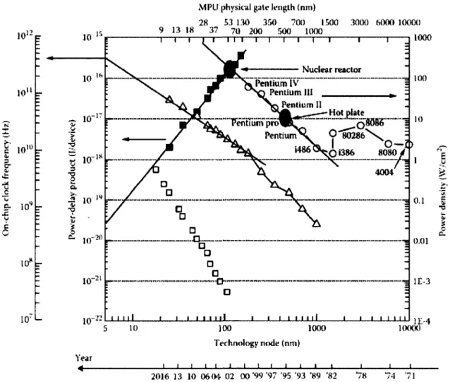
Figure 1.2 Power dissipation as a function of generation node. Power density on the surface of
current and past microprocessor generations (open circles), on-chip clock frequency (open triangles), power-delay products for a single device (solid squares), estimated power density for the basic switch with linear driving function (open squares). [Goddard III et al., May
2007] 2
Figure 1.3 Nanoelectronics Technology Development Paths [ITRS, 2009b] 3
Figure 1.4 Equivalent circuit of a multigate SET 7
Figure 1.5 Gate-voltage vs. drain current characteristics of a multigate SET 8
Figure 1.6 Stability diagram of a SET 9
Figure 1.7 (a) Schematic of single electron transistor used to simulate characteristics curves (b)
Ids vs Vds SET characteristics as the gate voltage Vgs varies from 0 V to 1.6 V in 0.4 V steps,
(c) & (d) Coulomb oscillations in I<jS vs Vgs as Vds varies from 0 to 2 V in 0.2 V steps.
Circuit parameters: Cs = Cd = Cj = 0.03 aF, Cg = 0.045 aF, Cb = 0.05 aF, R, = 1 Mil,
T = 300 K 11
Figure 1.8 Schematic diagram of future SET/CMOS hybrid LSI [Uchida et al., 2002] 13
Figure 2.1 (a) SET junction sketch (b) circuit symbol for SET junction 22
Figure 2.2 Thevenin equivalent of the circuit seen from a tunnel junction 25
Figure 2.3 (a) inelastic tunneling (b) elastic tunneling 27
Figure 2.4 SET model comparison, MIB [Mahapatra et al., 2004] and Xuan et al. [Xuan et al.,
2009]. (a) SET inverter schematic with simulation parameters (b) transient characteristics at different capacitive load (c) delay curves with different capacitive load 31
Figure 2.5 (a) SEM of a SET in SOI. (b) Schematic diagram [Ali et Ahmed, 1994] 35
Figure 2.6 (a) Schematic of a SET by PADOX (b) Typical conductance oscillations of a SET
as a function of gate voltage at various temperatures and at a drain voltage of 10 mV
[Takahashi et al., 2000a] 36
Figure 2.7 Fabrication process of single electron transistor based on silicon nanocrystal [Dutta
Figure 2.8 SET schematic 38
Figure 2.9 (a) Photo mask for 36 SETs with MIM and TLM structures (b), (c), (d) Zoomed
images of (a) (SEDIMOS project documentation) 39
Figure 2.10 SET trench formation (SEDIMOS project documentation) (a) First EBL (b) Si02
dry etch 40
Figure 2.11 SET Ti island and gate formation (SEDIMOS project documentation) (a) Second
EBL (b) Ti deposition (c) Lift -off. 41
Figure 2.12 SET tunnel junction formation, oxidation (SEDIMOS project documentation) 41
Figure 2.13 SET Source and Drain formation (SEDIMOS project documentation), (a) Ti
deposition (b) CMP 42
Figure 2.14 (a) SET inverter circuit (b) Implementation of SET inverter [Heij et al., 2001] (c)
Input-output characteristics of the inverter are plotted for two values of the induced charge difference. The solid lines are simulations using the orthodox theory for single-electron
tunneling [Heij et al., 2001] 43
Figure 2.15 Complementary SET gates, (a) NAND gate (b) NOR gate 44
Figure 2.16 Merged SET-MOSFET inverter circuit 45
Figure 2.17 Equivalent circuit of (a) a multigate SET and (b) its operation principle. Drain
current Id at small drain voltage depends on the number of electrons in the SET island, which is determined by the summation of the products of each Cgj and Vjnj. Id is minimum
when the number of electrons in the island is an integer [Takahashi et al., 2000b] 46
Figure 2.18 (a) SEM images of 2-input-gate XOR SET structure (b) current switching characteristics of a structure when the input-gate voltages (Vinl and Vin2) were switched between 0 and 0.2 V. The measurements were made at 40 K and a drain voltage of 10 mV
[Takahashi et al., 2000b] 46
Figure 2.19 (a) Schematic of the universal literal gate [Inokawa et al., 2001b] (b) Id - Vjn
characteristics, which are almost completely independent of Vout since the VdS of the SET is
kept nearly constant at Vgg minus V,h, the threshold voltage of the MOSFET (c) Expected
transfer (Vout - Vjn) characteristics 47
Figure 2.20 Complementary SET static memory cell (flip-flop) [Korotkov et al., 1995] 48
Figure 2.21 (a) Multiple-valued memory schematic (b) 2-terminal I-V characteristics of the
combined SET-MOSFET circuit with the SET gate shorted to the MOSFET drain [Inokawa
Figure 2.22 (a) A multiple-valued single electron SRAM cell with two depletion-mode
MOSFETs (Ml and M2 ) and one enhancement-mode MOSFET (M3). (b) An
example of the SRAM layout [Inokawa et al., 2003] 50
Figure 2.23 (a) Schematic of a cell CAM cell (b) Architecture of a
two-bit-per-cell CAM [Degawa et al., 2005] 51
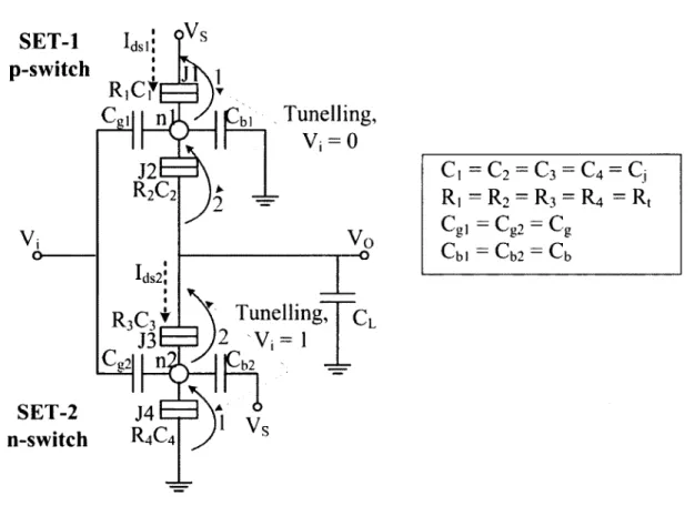
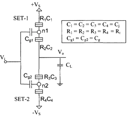
Figure 3.1 SET (2 gates) schematic 62
Figure 3.2 SET inverter circuit. Assumed parameters: Vs = Vj "high' - 800 mV, Vj "low" = 0
V, gain - 1, T = 300 K, Rt = 1 MQ. Derived parameters: Cj = 0.03 aF, Cg = 0.045 aF, Cb
= 0.05 aF (all within fabrication range) 64
Figure 3.3 (a) SET inverting voltage gain (at T = 300 K) & maximum operating temperature
(e2/2Qr = 40 KbT ) as a function of gate capacitance Cg, device parameters: Cj = 0.03 aF, Cb
= 0.05 aF (b) SET inverter maximum operating temperature as a function of tunnel junction capacitance Cj (e2/2Cx = 40 KbT ), device parameter Cb = 0.05 aF, (all capacitances within
fabrication range) 67
Figure 3.4 SET inverter delay & -3 dB Bandwidth as a function of tunnel resistance Rt, device
parameters: Q = 0.03 aF, Cg = 0.045 aF, Cb = 0.05 aF, T = 300 K, Vs - Vj "high" = 800 mV,
Vj "low" = 0 V, gain = 1, CL = 40 aF 68
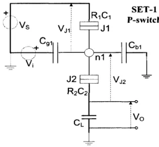
Figure 3.5 SET-1 and SET-2 (figure 3.2) stability diagram with oscillations characteristics .... 69 Figure 3.6 The p-switch (a) circuit diagram (b) stability diagram (c) transfer characteristics... 71
Figure 3.7 The p-switch, circuit to calculate the tunnel junction voltage 74
Figure 3.8 Then-switch (a) circuit diagram (b) stability plot 76
Figure 3.9 The n-switch, circuit diagram to calculate the tunnel junction voltage 78
Figure 3.10 SET inverter transfer characteristics 79
Figure 3.11 SET inverter circuit - Bipolar input-output voltage response. Assumed parameters:
±Vs = ± 400 mV, gain = 1, T = 300 K, Rt = 1 MQ. Derived parameters: ± Vj = ± Vo = ±
200 mV, Cj = 0.05 aF, Cg = 0.1 aF (all capacitances within fabrication range) 91 Figure 3.12 SET inverter unipolar transient analysis. Supposed parameters: Vs = Vj "high" =
800 mV, Vj "low" = 0 V, gain = 1, T = 300 K, R, = 1 MQ; Derived parameters: Cj = 0.03 aF,
Cg - 0.045 aF, Cb = 0.05 aF 94
Figure 3.13 SET inverter bipolar transient analysis. SET parameters: Supposed parameters:
±VS = ± 400 mV, gain = 1, T = 300 K, Rt = 1 MQ; Derived parameters: ±Vj = ±Vo = ±200
Figure 4.1 SET build-up BEOL compatible 3D technology 100
Figure 4.2 Wafer level 3D technology [Lu et al., 2007], (a) via-last, oxide-to-oxide bonding, (b)
last, adhesive (polymer) bonding, (c) first, copper-to-copper bonding, and (d)
via-first, metal/adhesive redistribution layer bonding 101
Figure 4.3 Hybrid circuit simulation flow flowchart 103
Figure 4.4 The nominal Ids-Vds curves of 22 nm planar bulk CMOS devices 105
Figure 4.5 NMOS (22 nm PTM planar bulk model) gate length = 21 nm and width = lum
simulated Ids-Vds curves compared with ITRS predicted NMOS saturation drive current for
21 nm technology node 105
Figure 4.6 SET inverter transient analysis. SET parameters: Vs = Vj "high" = 800 mV, Vj "low"
- 0 V, gain = 1, T = 300 K, Rt = 1 MQ, Cj = 0.03 aF, Cg = 0.045 aF, Cb = 0.05 aF 106 Figure 4.7 SET inverter transient analysis. SET parameters: Supposed parameters: ±VS = ±
400 mV, gain = 1, T = 300 K, R, = 1 MQ; Derived parameters: ±Vj = ±V0 = ±200 mV, Cj
= 0.05 aF, Cg = 0.1 aF 107
Figure 4.8 Transient analysis (a) NAND gate (b) NOR gate. Circuit 2.15 parameters: Vs = 800 mV, Vgi = gnd, Vg2 = 800 mV, A = input 1 and B = input 2 as in graph above 108 Figure 4.9 (a) SET-MOSFET inverter (b, c) simulation waveform. Circuit parameters: Vs =
Vj„ "high" = 800 mV, Vin "low" = 0 V, T = 300 K, R, = 1 MQ, Cj = 0.03 aF, Cg = 0.045 aF,
Cb = 0.05 aF, PMOS 22 nm planer bulk model 109
Figure 4.10 (a) Schematic of the universal literal gate (b) Id - Vin characteristics, (c) transfer
characteristics. Circuit parameters: Vg = 800 mV, Rt = 1 MQ, Cj = 0.09 aF, Cg = Cb = 0.19
aF, Vg = 330 mV, 310 mV, 280 mV, 270 mV (from blue to black lines), MOSFET 22 nm
planar bulk model 110
Figure 5.1 Hybrid SET-CMOS cascaded inverter with interconnect parasitics. (a) Model (b)
Circuit diagram 113
Figure 5.4 Transient analysis (figure 5.1 (b)). Parameters: Cj = 0.07 aF, Cg = 0.045 aF, Cb =
0.05 aF, Rt = 1 MQ, T = 300 k, Vs = Vj "high" = 800 mV, Vj "low" - 0 V, SET inverter
gain 0.56, parasitic same as calculated in section 5.2.2 121
Figure 5.5 Hybrid SET-FET inverter (figure 5.1 (b)) simulation result for varying tunnel
junction resistance. Parameters same as in figure 5.4. (a) -3 dB bandwidth vs interconnect
Figure 5.6 SET inverter Fanout (a) Circuit diagram (b) Circuit with parasitic (used for
simulation) (c) Model for SET layer on CMOS carrier (22 nm node). Metallic SET features BEOL fabrication and hence offers low costs and low thermal budgets without using effective silicon area. For functional and heterogeneous 3D integration of nanoelectronic devices, SET circuits can be stacked above the CMOS platform. For SET-CMOS hybridization, CMOS is essential for I/O, signal restoration and to maintain compatibility
with established technology 129
Figure 5.7 Layout to study SET inverter driving capability consisting of SET inverters with Ti
interconnect. Interlayer capacitance is marked blue and green. Blue is between Ti interconnect and green is between Ti interconnect and the source of SET which is also Ti. Resistance for interconnect is considered throughout the length of Ti wire 131
Figure 5.8 Interconnect capacitance layer 132
Figure 5.9 (a) SET interconnect layout for minimum interlayer capacitance (b) SET interconnect
layout for maximum interlayer capacitance 133
Figure 5.10 Schematic of a single SET inverter driving 8192 SET inverters with Ti interconnect
parasitic 135
Figure 5.11 Simulation result for the circuit in figure 5.6 (b). SET parameters same as derived
in 3.2.7. (a) D.C. analysis (b) Transient analysis 135
Figure 5.12 SET fanout simulation in Cadence environment, effect of varying load on delay &
bandwidth. SET parameters: Vs = Vj "high" = 800 mV, Vj "low" = 0 V, gain = 1, T = 300
K, R, = R2 = R3 = R4 = 1 MQ, Ci = C2 = C3 = C4 = 0.03 aF, Cg) = Cg = 0.045 aF, Cb) = Cb2
= 0.05 aF 136
Figure 5.13 Simulation setup to compare SET inverter and a CMOS inverter 138
Figure 5.14 Simulation results to compare SET and CMOS logic, Transient analysis 139
Figure 5.15 Circuit diagram to increase SET logic driving capability, parallel connected SET
inverters driving CMOS plus interconnect load 141
Figure 5.16 Delay analyses to improve SET logic efficiency for the circuit in figure 5.15.
Parameters: Cj = 0.07 aF, Cg= 0.045 aF, Cb = 0.05 aF, R, = 1 MQ, T=300 k, Vs = Vin "high"
= 800 mV, Vin "low" = 0 V, CMOS inverter - 22 nm BSIM predictive model [Cao et Zhao,
Table 1.1 Emerging nanodevices 4
Table 1.2 SET-CMOS high performance circuit examples 14
Table 3.1 SET device feasible parameter range and capacitance calculation 63
Table 5.1 Dimensions at 22 nm for different layers in CMOS IC 114
Table 5.2 Ti interconnect parasitic calculation 116
Table 5.3 Power consumption by SET and CMOS inverter in hybrid circuit (figure 5.1 (b))... 119 Table 5.4 Delay measurement to show improvement in SET logic performance by design
considerations 123
Table 5.5 SET device (figure 3.1) capacitance calculation 130
Table 5.6 Interlayer and lateral crosstalk capacitance calculation for Ti interconnect 134
Table 5.7 Power calculation for SET inverter driving capability circuit in figure 5.6 (b) 138
c
Capacitance [F]Cj,
c
s
Junction capacitance at the source [F] Cj,c
d
Junction capacitance at the drain [F]Cg
Control gate capacitance [F]Cb Tuning gate capacitance [F]
c
s
Sum of capacitances [F]CL Load capacitance [F]
Rt) R-s Tunnel resistance at the source [Q] Rt, Rd Tunnel resistance at the drain [£2]
Rk Quantam resitance ~ 26 kQ
Vds Voltage between drain and source [V] Vgs Voltage between gate and source [V] Vs Positive supply voltage [V]
Vi Input voltage [V]
V0 Output voltage [V]
Tunnel junction voltage [V] Vc Critical voltage [V]
Av SET interter voltage gain
Ids SET drain to source current [A]
Ec Charging energy [eV]
KB Boltzmann constant
T Absolute temperature [K]
e elementary charge
t time (s)
h Plancks constant
F free energy [eV]
ATBs Asymmetric Tunnel Barriers
CAD Computer Aided Design
CAM Content-Addressable Memory
CMOS Complementary Metal Oxide Semiconductor CMP Chemical Mechanical Polishing
CNT Carbon NanoTube
CRN2 Nanofabrication and Nanocharacterization research center
EBL Electron Beam Lithography
EOT Equivalent Oxide Thickness FET Field Effect Transistor
FQRNT The Fonds quebecois de la recherche sur la nature et les technologies GUI Graphical User Interface
IC Integrated Circuit
IMOS Ionization MOSFET
INL Institut des Nanotechnologies de Lyon.
ITRS International Technology Roadmap for Semiconductors LSI Large Scale Integration
MC Monte Carlo
ME Master Equation
MOSFET Metal Oxide Semiconductor Field Effect Transistor MTJs Multiple Tunnel Junctions
MtM More than Moore
MVL Multiple Valued logic
NDR Negative Differential Resistance PADOX PAttern Dependant OXidation
SEDIMOS Single Electron Device Integration On CMOS Technology SEM Scanning Electron Microscope
SIMOX Separation by IMplantation of OXygen
SOI Silicon On Insulator
TFET Tunnel Field Effect Transistor UdeS Universite de Sherbrooke
1.1 Future of microelectronics and nanoelectronics
The Moore's law has guided targets for the semiconductor industry for the last 40 years. The international technology roadmap for semiconductors (ITRS) predicts the technical capability the industry needs to stay on Moore's law. For several decades planar CMOS technology has been the workhorse for IC designers. It has been scaled as per Moore's law resulting in ever decreasing device size and in a number of technology nodes, the present being 32 nm. The ITRS predicts that the end of MOSFET scaling will arrive in 2024 with a 7.5 nm process [ITRS, 2009a]. Getting to 7.5 nm presents some long term difficult challenges such as continued scaling of multigate devices in aspects of equivalent oxide thickness (EOT), junctions, parasitic resistance, contact silicidation, mobility enhancement, and a number of problems as shown in figure 1.1. In addition to below mentioned scaling problems, the most worrisome
JUNCTION
GATE Lithography Gate depletion Gate resistance Shallow Junction formation
Junction resistance Contact resistance GATE DIELECTRIC Gate-dielectric tunneling Dopant penetration WIRING CHANNEL Wire resistance Interconnect capacitance Elect romigration Crosstalk noise
Random dopant distribution Inversion-layer capacitance Punch-through
Direct source-drain tunneling
Figure 1.1 Problems in the Scaling of MOSFETs [Oda et Ferry, 2006]
technological challenges would be increased power dissipation, integration density, shrinking noise margin in addition to cost increase in lithography. Despite the decrease in power for a single device, increase in power dissipation is governed by technology miniaturization, which allows for higher integration density and faster switching speed as shown in figure 1.2.
10l2tr 10' c 10" ft. 3 c* o> 10 10" 10* i—
MPU physical gate length (nm)
28 53 130 350 700 1500 9 13 18 37 70 200 500 1000 TTT—I—T 50(H) (>1)00 10000 1000 = 100 Nuclear reactor Pentium IV Pentium 1IJ Pentium II Hot plate Pentium pro Pentium^ O'80286>sS.
I
o
I486 i386 8080 400* : i i 111 i 111 « 0.01 - IE-3 1E-4 10000 Year 4— Technology node (nm) J I—J I I I I I L JL 2016 13 10 0604 02 00'99 '97 '95 '93 '89 '82 18 74 '71Figure 1.2 Power dissipation as a function of generation node. Power density on the surface of
current and past microprocessor generations (open circles), on-chip clock frequency (open triangles), power-delay products for a single device (solid squares), estimated power density for the basic switch with linear driving function (open squares). [Goddard III et al., May 2007]
From this, it is evident that CMOS scaling will likely become very difficult with a need to augment the capability of CMOS by introduction of novel devices and new information processing architectures. Post-CMOS devices must further reduce the cost and increase the performance of IC's. The parallel rise of new technologies shall evolve new manufacturing and design paradigms in addition to new devices. The advancement is anticipated in 2 phases. First phase would be heterogeneous integration of new technology with CMOS to add functionality to that attainable by ultimate CMOS. The second phase would advance this technology to realize a new multifunctional scalable platform. Research in nanoelectronics envisions extending CMOS
and proposes new devices and technologies that perform either processor or memory functions or both in universal devices.
The direction for further progress and research in future ICs can be separated into 3 main domains (figure 1.3), (i) "More Moore", (ii) "More than Moore", and (iii) "Beyond CMOS". Moore's law applies only to (i), while (ii) and (iii) abstains from it and aggressive scaling is no longer the driving constraint. "More Moore" considers CMOS miniaturization at lower cost, higher performance and lower power dissipation, as seen by the semiconductor market trend for the previous 40 years. The second trend "More than Moore" (MtM) encompasses the hetero geneous integration of digital and non-digital functionalities into compact systems. "Beyond CMOS" is characterized as the capability to scale the performance of ICs beyond the ones attained by ultimately scaled CMOS. Some examples are carbon-based nanoelectronics, spin-based devices, and ferromagnetic logic.
More than Moore
Function diversification route (non-scaling) of electronic devices: Integration of non-digital components into electronic devices
| Functional Diversification (More than Moore),
More Moore SILICON NANQ-CMOS Miniaturization (scaling) route along CMOS technology for CPU, Memory, Logic Stntort AnaloprRF K Pm«1vm lnt»«»ctlftg wtth p+opt* *nd »nvironmtnl Noo-iOgfW cofftoftf Systom~in-p*cM*9* (StP) mformtoort Ptoc—tino CHgtw content Syst*n-ot*<hip (SoC) 32nm Beyond CMOS Heterogenous integration for High Value Systems System-on-chip (SOC) + System-in-package (SiP) = digital + non-digital Beyond CMOS NON-SILICON CMOS
Alternative disruptive non-CMOS technologies to achieve same or improved performance of electronic devices
1.2 Potential nanoelectronics devices and application areas
Nanoelectronics typically encompasses devices and technology in which the critical dimension is less than 100 nm and governed by new physical phenomenon (quantization of channel charge in MOSFET or Coulomb blockade effect in quantum dot). The device exhibits unparalled electrical or optical or mechanical properties due to its nanoscale dimensions and hence encourages the discovery of new paradigms for information processing. It focuses on engineering aspects to produce such components and applies it to micro or nanodevices / systems for various applications. ITRS organizes emerging nanodevices into 3 categories as below [ITRS, 2009c],
Table 1.1 Emerging nanodevices Category 1
MOSFETs, Extending the channel of MOSFETs to the End
of the Roadmap Category 2 Unconventional FETS, Charge-based Extended CMOS Devices Category 3 Non-FET, Non Charge-based 'Beyond CMOS' Devices
CNT FETs Tunnel FET Collective Magnetic Devices
Graphene nanoribbons I-MOS Spin Transfer Torque Logic
III-V Channel MOSFETs Spin FET Moving domain wall devices
Ge Channel MOSFETs SET Pseudo-spintronic Devices
Nanowire FETs NEMS switch Nanomagnetic (M:QCA)
Non-conventional Negative Cg MOSFET Molecular Switch
Geometry Devices Excitonic FET Atomic Switch
Mott FET
[ 1 ] E x t e n d i n g t h e c h a n n e l o f M O S F E T s t o t h e e n d o f t h e r o a d m a p : Nanodevices in this
category lists MOSFET structures that use field effect functionality to modulate the flow of current. They may use alternate channel material offering a higher quasi-ballistic charge carrier velocity and higher mobility than strained silicon or different geometry with parameters relevant to high and general performance logic. Introduction of materials like strained Ge, SiGe, III-V compound semiconductors, CNTs and graphene offers rich physics that may enable development
of a new information-processing device. The technology is fraught with several very difficult material, process and device challenges.
[2] Extended CMOS (Charge-Based): These set of devices specially offer co-integration
with CMOS platform, to extend the functionality of ultimately scaled CMOS. A hybrid integrated system of nanoelectronic devices is built to enhance CMOS. They offer lower power dissipation by providing a steeper sub threshold turn-on current voltage characteristic (S < 60 mV/decade). One such device is the tunnel FET (TFET). In TFETs, the channel current is modulated via a source-channel tunnelling process in a FET-like device structure. Limitations of the TFET include low on current (Ion), development of device modeling and a hypersensitivity to structural and material variations.
The second device is the impact ionization MOSFET (IMOS) wherein, impact ionization generation of channel charge modulates the channel current. Because of its higher-impact ionization-generation rates and reduced breakdown voltages, there is an increase in the device drivability and scalability. The challenge with this device is the possibility of high density integration. The third device, negative gate capacitance (Cg) MOSFET is obtained by replacing the insulator of a MOSFET gate stack with a ferroelectric insulator to implement a step-up voltage transformer that will amplify the gate voltage. The device operates with low-voltage and low power because of the sub threshold slope lower than the classical limit of 60 mV/decade. The challenges include, the negative capacitance if achieved, is not enough to realize a high performance switch and the response time of the polarization in ferroelectric gate dielectric.
The next in this category is the spin transistor, divided into 2 groups, FET and spin-MOSFET with different operating principle. The source and drain of both devices are composed of a ferromagnetic material. The switching operation in spin-FET is achieved by spin precession or dephasing of spin-polarized charge carriers injected into the channel while in spin-MOSFET, relative magnetization configurations of the source and drain are used to modify the output. Although the spin-MOSFET has not been realized, the key challenge is injecting a high percentage of spin-polarized electrons from a half-metal source into the channel, and how these devices interconnect. One more addition to the list is NEMS switch facing a major challenge for
volt level operation at GHz switching speed. Finally the device of our concern, the single
electron transistor (SET) can potentially deliver high device density and power efficiency at
good speeds if the issues of large threshold voltage variation and low current drivability can be solved. In this work, we have investigated and showed for the first time a systematic approach to
analyse, design, and simulate large scale SET / hybrid SET-CMOS circuit at 22 nm node validating SET logic driving capability with CMOS comparable output voltage and GHz frequency at room temperature.
|3] Beyond CMOS (Noncharge-Based) Devices: Logic devices evaluated in this section
are novel devices for more specialized tasks like associative processing, communication, multi valued logic and ferromagnetic elements for non-volatility, radiation hardness and error tolerance. They demand architectures other than von Neumann. They are collective spin device, moving domain wall devices, atomic switches, molecular devices, pseudospintronic devices, Bilayer pseudoSpin Field-Effect Transistor (BiSFET), nanomagnetic logic devices. Each of these devices offers a common advantage of reduced power dissipation, but each has several challenges.
1.3 Single electron transistor and its hybridization
Many potential alternatives to beyond CMOS technologies for logic applications include ID structures, channel replacement materials, single-electron transistor, molecular devices, ferromagnetic devices, and spin transistors. Such device circuitry will encounter limitations in interfacing with the external world, and hence must be integrated with conventional CMOS for I/O, functional and technology based limitations. The terascale level of integration of such devices with CMOS helps to realize substantial gains in power dissipation, performance, or density. While many of these promising technologies are on the horizon, they are abounded with variability, manufacturing challenges, and confined by existing CMOS manufacturing infrastructure. The candidate technology must have scalable potential greater than CMOS, low energy consumption for anticipated device density, room temperature operation, switching speed that can compete or outperform CMOS. From recent research, literature studies and ITRS update
2010, the use of a SET as a potential building block for future hybrid circuits is confirmed and justified These CMOS-SET hybrid systems represent an opportunity to leverage the immense infrastructure and computational power of modern CMOS while also taking advantage of the SET's unique functionalities. From this research, it will not be an exaggeration to say that, in a longer term, a new SET based information-processing technology might become dominant by adding new functionality (both logic and memory) in back-end-of-line (BEOL) CMOS process.
1.3.1 Concept of single electron transistor
After introduction of a SET transistor by Likharev in 1987 [Likharev, 1987] there have been many publications related to its applicability in LSI systems. Thesis and books [Visscher, 1996; Mahapatra et Ionescu, 2006a; Wasshuber, 2001] are recommended for historical reviews, further reading and approaches to SET, since we present only the theory that is relevant to the functional behaviour of a SET. The unit cell of a SET is a nanoscale sized tunnel junction (barrier) which consists of two conductors separated by a thin oxide. The device as shown in figure 1.4 contains a small island together with one or more gate electrode coupled capacitively to the island. The source and the drain electrodes are attached to the island via a tunnel barrier. Here, Cs and C<j are the tunnel junction capacitances and Rs and Rd are the tunnel junction
Source
Gates
O O O 'glC
g2 a g3Island
C
SR
S" C
dR
dTunnel Junction
Drain
Figure 1.4 Equivalent circuit of a multigate SET
ITRS 2011 reports that SET has been dropped from Emerging Research Devices due to insufficient research activity.
resistances. The operation principle of a SET is a charge balance between the gate electrode and the island coupled by a capacitor Cgj. This research is focussed on a room temperature operating
metallic SET with capacitively coupled gate (C-SET) fabricated by the nanodamesence process at UdeS [Dubuc et al., 2008]. In this thesis, we shall consider symmetrical C - SET, meaning Cs
= Cj = Cj and Rs = R(/ - R,, with one control gate Cgi = Cg and a tuning gate Cg2 = Ch- More
details on fabrication and operation of the metallic SET is covered in chapters 2 and 3 respectively.
The current through the SET consists of electrons tunnelling through the source to the island and from the island to the drain terminal. To understand its working principle, the source and the drain terminals are grounded. By applying a voltage Vgi to the ith gate, a charge of CgjVgj
is accumulated at the gate electrode resulting in a total charge of XCgjVgi at the gate. If the total
charge of -ne ("n" is the number of electrons, "e" is the elementary charge) on the island is balanced with that in the gate, then £CgiVgj = ne is satisfied. In this condition, since the number
of electrons, n is stable, no current flows through the island. This is known as the Coulomb blockade. Further increase in the gate voltage increases total charge on the gates and the charges become unbalanced. With ]TCgiVgj = (n+l/2)e, the electrostatic potential for n electrons and n+1
electrons becomes equal, which implies n or n+1 electrons in the island. When a small voltage is applied between the source and drain electrodes, electrons flow from the source to the island
>
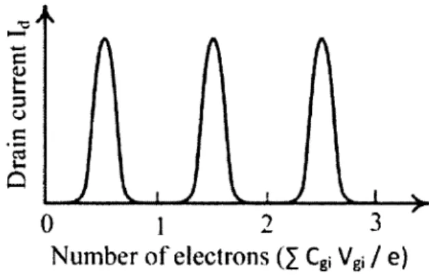
0 ) 1 2 3
Number of electrons (I C
gi V
gi/ e)
leaving n+1 electrons in the island. The number of electrons in the island returns to n, once an electron has tunnelled from the island to the drain. The current hence flows due to single electron tunnelling by repeating these steps. With further increase in the gate voltage, n+1 electrons becomes stable. This causes periodic characteristics of the source-drain conductance as a function of the gate voltage, as depicted in figure 1.5.
It is possible to define the transport regions of a SET as a function of the drain-source voltage, Vd and the gate voltage Vg (with capacitance Cg). Such a conductance plot as a function
of both Vd and Vg is known as a stability diagram, as shown in figure 1.6. In the diagram, the
Coulomb blockade occurs inside the diamonds, hence called Coulomb diamonds. They are the stable regions with the number of electrons (n) in the island with a periodicity of e/Cg along the
\ Unstable
JK region
non-inverting gain (Avi)
^ Unstable region Ids - const/""
diverting gain (A|)
n = -l n = 0
Stable region^/ y ^ Stable region Stable rc gion
Unstable region Unstable
region
~0
Figure 1.6 Stability diagram of a SET
Vg axis of the stability diagram. Outside of Coulomb diamonds the number of electrons
fluctuates between certain integers in the island. In the adjacent regions, a fluctuation by only one electron charge is possible. As there are electrons passing through the island one after the other, these are the regions of single-electron tunnelling. The slope of the graph 1.6 defines the maximum inverting voltage gain (A]) and the non inverting gain (AVi) which are defined by SET
Inverting gain, Ai = Cg / Cj
Non-inverting gain, Avi = Cg / (Cg + Cj)
(1.1)
(1.2)
These equations identify the possibility to obtain Ai greater than 1 by designing and fabricating Cg > Cj. Hence, similar to CMOS logic, logic circuits based on SET inverter with gain greater than one can be made. More details based on designing SET logic with parameters like gain,
temperature, delay and bandwidth shall be discussed in chapter 3.
Figure 1.7 (b) shows a simulation result of Ids - Vds characteristics and figure 1.7 (c) and (d) shows the IdS - Vgs of a SET circuit (figure 1.7 (a)) with the parameters derived in section
3.2.7 at 300 K using the simulation method developed in section 4.5. The Ids - Vds is plotted as
Vgs is varied from 0 V to 1.6 V. The width of the Coulomb gap reduces from a maximum to zero. In the Ids - Vgs characteristics of figure 1.7 (c) and (d), the current as seen in the coulomb
oscillations increases in magnitude as VdS increases. The period is AVg = e/Cg = 3.55 V. Such
periodic function is not possible in conventional devices and it is useful in logic circuits like adder or parity check circuits.
As an emerging technology and with the advancements in fabrication technology, SET offers a greater scaling potential than CMOS as the device properties depend basically on the nanoscale sized tunnel junction. The operation principle confirms that the performance of SETs will improve as their size is reduced, in contrast to MOSFETs that require complicated structures and dopant profiles as the device size is reduced. It is expected that the circuit design with such a device shall be characterized by "functional integration" which will reduce the number of interconnections and devices in a basic building block. A SET circuit consumes less energy than CMOS and can be fabricated with conventional lithography technology in silicon. The literature study limits its operation to cryogenic temperatures. Although SET device is a fast switching device (when driving load less than its total capacitance), all recent research limits its full potential due to low current drivability.
(a)
Source Drain < 150 600 • 400-200-<
c 0-v » -200- -400-j -600-.*>(b)
V = 0 V ds = 0.2 V = 0.4 V = 0.6 V -V = 0.8 V ds = 0.8 V- v ,
= 1 V V, (V) as v < c 600 500 400 300-200 V = 0 V V = 0.4 V ** V = 0.8 V s* V = 1.2 V V Si = 1.6 V —t 2 (C) V (V) gs v ' V,K = 1.2 V V„ = 1.4 V V* = 1.6V Vas = 1.8 V 2 VSETs can be applied to general purpose Boolean logic, but significant circuit and architecture study will be required to exploit its full potential. Because of the SETs capability for room temperature operation [Dubuc et al., 2007], they have a promising application in high density memory and logic circuits with conventional silicon LSI processing techniques. Companies like Hitachi Inc., Toshiba, and Agilent Technologies have already demonstrated single-electron memory and have in their roadmap a planned production in the 2010 to 2015 time frame. Other possible applications of SETs include: metrology for precision measurements, logic circuits, Microwave detector, and magneto electronics.
1.3.2 SET hybridization
It is believed that through the integrated approach of CMOS-hybrid systems, new dimensions of functionality and value in integrated circuits and systems can be achieved. The SET and CMOS have complementary properties. The SET disadvantages of low current drive and high output impedance can be compensated by CMOS high gain and current drive, high input impedance, and mature fabrication technology. At the same time the CMOS drawback of scaling further to sub-10 nm physical limits (particularly, the tunneling currents increases with the increase in the temperatures and gate voltages, resulting in significant contribution to the subthreshold current even at 300 K) and power density can be overcome by nanoscale SET device functionality, or programmability due to coulomb blockade oscillations and its ultra low power dissipation. Moreover, room temperature operation of a SET is not a major issue now [Dubuc et al., 2007], Hence the near future foresees SET-CMOS hybridization [ITRS, 2009a; Wasshuber, 2003; Ionescu et al., 2002]. This brings new functionalities with few devices, unmirrored in pure CMOS through SET-CMOS hybridization done in BEOL.
SET Low-power
Logic
CMOS
Memory High-speed CMOS Logic
Single-electron Programmable Logic Array
(PLA)
Figure 1.8 Schematic diagram of future SET/CMOS hybrid LSI [Uchida et al., 2002]
To study the feasibility of hybrid SET-CMOS circuit at room temperature, SET logic and CMOS inverter were fabricated on the same chip and its operation demonstrated at Advanced LSI Tech Lab, Toshiba Corp, Yokohama, Japan [Uchida et al., 2002], They presented future prospect on hybrid SET/CMOS LSI (figure 1.8) wherein, SETs are used in a programmable low power block and CMOS is used in a high speed I/O circuit block. Table 1.2 illustrates SET-CMOS high performance circuits with novel functionality which cannot be attained by any other alternative. The proposed hybrid SET-CMOS logic circuits offer high current drivability, reduced number of conventional devices, low power dissipation and much less area compared to CMOS. For room temperature operating SETs, such a high performance hybrid circuit should not be far from the reality.
Table 1.2 SET-CMOS high performance circuit examples.
Quantizer [Inokawa et al., 2003] Multi peak NDR device / Multiple
value logic / SRAM cell
[Inokawa, Fujiwara et Takahashi, 2001c] I — I I
dd CLK
•wr J
MOSFET uk. r MOSFET transfer-gate MOSFET SET3-bit ADC [Inokawa et al., 2003]
CLK we m* M1 m' h «en
quantizer
2C, 1C. c±Parallel SETMOS with three-gate SET transistor as
AND, NOR and XOR gate [Deng et al., 2009] 1 bit Full adder [Sui et al., 2010]
^ "it—i dci OUT V PS-SET ci to in-a •GJ ._) |—i v, CI
1.4 Open questions and Project objectives
Heterogeneous 3D integration and functional integration of nanoelectronic devices, memory elements, and interconnects are possible solutions to future silicon technology challenges which are limited by increased power dissipation and thermal heating due to continuous scaling. We have seen that the SET is a potential building block for future hybrid nano-CMOS circuits. In such a circuitry, the SET can perform new functionalities such as reconfigurable logic, random number-based circuits, and multiband filtering circuits that can combine with CMOS based general purpose processors or I/O signal restoration [ITRS, 2009a], It is hence necessary to develop and adopt a generalized but systematic design methodology for such hybrid circuits at a specific technology node for room temperature operation. Moreover, SET use in commercial ICs is questionable, specifically at the SET-CMOS interfacing unit. In order to make such hybridization possible, it is necessary to prove SET logic driving capability for CMOS with sufficient current drive and output voltage. The core SET logic can be designed to operate at low voltage, nevertheless, at the interface the output of the SET logic must be in a voltage range that can be fed to a CMOS input for proper logic functionality. More importantly, a recent breakthrough at UdeS [Dubuc et al., 2007] has enabled to show the first true demonstration that a metallic SET can operate under normal electronic circuit conditions and even at temperatures exceeding 130° C. Indeed, this type of device must normally be cooled at temperatures much below the normal operation temperatures of a standard microelectronic circuit in order to benefit from its unique nanoscale properties. The SET transistors are fabricated using CMOS BEOL-compatible processing; hence the SET circuits can be easily stacked above the CMOS platform. This decreases the interconnect parasitics and increases the density of functions, improving yield at lower cost and thermal budget of highly integrated systems.
As a consequence, a new undertaking of a project "SEDIMOS" between UdeS, Institute of nanotechnology (INL), Lyon, France and STMicroelectronics, France has been signed, to further explore fabrication and working of SET and SET-CMOS hybrid circuits. The purpose of this thesis is to research the possibility of realizing hardware support for such circuits by first, presenting a design and simulation method for a large scale integrated circuit. The designed logic can be used as a building block for other logic applications. The design methodology and
simulation method presented in this thesis can be adapted to any SET or hybrid SET-CMOS circuit. Following it, we have investigated the case of a SET-CMOS interface which exploits full potential of SET performance in terms of its CMOS driving capability and CMOS comparable output at GHz frequency voltage for room temperature operation, then provided design criteria and circuit architecture for delay improvement. The overall idea is to provide working model which proves SET logic efficiency in SET-only as well as hybrid environment, proving SET candidacy as an alternate device to CMOS in the long run.
Previous research and study related to SET technology and its future can be divided in 4 main categories. The first category which accounts for most of the research effort is in the field of device physics and device fabrication. The second research category focuses on the application of SET devices like logic and memory. The third category with a little amount of publications is at the level of circuits and system design. The fourth one, which accounts to the least amount of published research, is in the area of SET hybridization with the existing CMOS technology. Many unresolved issues in bringing this technology together need attention. The work presented here falls under 3rd and 4th categories. We present a vision that accounts to SET
technology hybridization and in long term as an independent technology. The SET-CMOS hybridization embraces the current and future scaling of CMOS by co-integration of SET to enhance new functionality and modality.
To study SET and its hybrid circuits, there have been simulation methods developed, but with some or other constraints in regard to design or simulation. The SET logic circuit simulation was limited to either: few devices and lacked in depth parametric analysis, tradeoffs in electrical and SET physical parameters and interconnect parasitics in addition to spice coding. A more
efficient simulation method which .can simulate large SET / hybrid SET-CMOS circuits, with speed and accuracy is required to study the full potential of such circuits. Hence the primary requirement of this study was to develop such a method in Cadence environment.
According to the literature study and as mentioned above the major obstacles for SET implementation both in SET only and hybrid circuits which restricts its application to commercial ICs are; its room temperature operation, low driving capability, and a very low
output voltage compared to CMOS. The SET electrical response depends on its physical fabricated parameters. It is difficult and a challenge to design SET parameters to attain CMOS like voltage and delay at room temperature in hybrid as well as SET-only circuits. No work demonstrated this capability nor suggested it could be possible. In order to achieve the designed response, difficult challenges related to implementation of SET or hybrid SET-CMOS based nanoelectronics can be divided into those related to:
1. Develop an efficient simulation method for large scale SET as well as hybrid SET-CMOS circuits,
2. Implement design consideration for SET-CMOS hybrid circuits based on SET physics and circuit theory and tradeoffs between different electrical and fabrication parameters to optimise hybrid SET-CMOS logic parameters,
3. Develop a design methodology (analytical) for hybrid SET-CMOS logic for its use in commercial ICs,
4. Design, simulation, and parameter optimization of integrated SET-CMOS hybrid circuits to study its efficiency,
5. Study hybrid SET-CMOS logic performance and driving capability in terms of delay, -3 dB bandwidth, gain, considering the interconnect parasitics effect at room temperature operation.
This leads to the following research questions:
1. Can we develop a simulation method for a SET and hybrid SET-CMOS logic in Cadence environment used for present LSI simulation? If yes, then is it possible to simulate such circuits at higher technology nodes, not supported by Cadence library? If made possible, validate the Cadence SET simulation by standard SET simulator (SIMON) along with CMOS definition at future node.
![Figure 2.4 SET model comparison, MIB [Mahapatra et al., 2004] and Xuan et al. [Xuan et al., 2009]](https://thumb-eu.123doks.com/thumbv2/123doknet/5410467.126269/54.914.187.703.125.996/figure-set-model-comparison-mib-mahapatra-xuan-xuan.webp)
![Figure 2.7 Fabrication process of single electron transistor based on silicon nanocrystal [Dutta et al., 2000]](https://thumb-eu.123doks.com/thumbv2/123doknet/5410467.126269/60.915.187.751.141.474/figure-fabrication-process-single-electron-transistor-silicon-nanocrystal.webp)
![Figure 2.14 (a) represents CMOS-type SET inverter proposed by Tucker [Tucker, 1992] together with experimental realization of the same by Heji et al [Heij et al., 2001] based on metallic tunnel junctions (figure 2.14 (b) and (c))](https://thumb-eu.123doks.com/thumbv2/123doknet/5410467.126269/66.916.133.787.678.961/figure-represents-inverter-proposed-experimental-realization-metallic-junctions.webp)