HAL Id: hal-00431019
https://hal.archives-ouvertes.fr/hal-00431019
Submitted on 10 Nov 2009HAL is a multi-disciplinary open access archive for the deposit and dissemination of sci-entific research documents, whether they are pub-lished or not. The documents may come from teaching and research institutions in France or abroad, or from public or private research centers.
L’archive ouverte pluridisciplinaire HAL, est destinée au dépôt et à la diffusion de documents scientifiques de niveau recherche, publiés ou non, émanant des établissements d’enseignement et de recherche français ou étrangers, des laboratoires publics ou privés.
WITH LOW VOLTAGE
Fabienne Pennec, David Peyrou, Dimitri Leray, Christina Villeneuve-Faure,
Anthony Coustou, Pierre-François Calmon, Patrick Pons, Robert Plana,
Fréderic Courtade
To cite this version:
Fabienne Pennec, David Peyrou, Dimitri Leray, Christina Villeneuve-Faure, Anthony Coustou, et al.. DC CONTACT MODELING OF ELECTROSTATICALLY ACTUATED SWITCHES WITH LOW VOLTAGE. 20th MicroMechanics Europe Workshop (MME 2009), Sep 2009, Toulouse, France. pp.B01, ID 113. �hal-00431019�
---
DC
CONTACT MODELING OF ELECTROSTATICALLY ACTUATED
SWITCHES WITH LOW VOLTAGE
F. Pennec
1, D. Peyrou
1, D. Leray
1, C.Villeneuve
1, A. Coustou
1, P. Calmon
1, P. Pons
1,
R.Plana
1and F. Courtade
21
LAAS – CNRS – Toulouse University, 7 av. du Colonel Roche-31077 Toulouse cedex 4
2
CNES - 18 av E. Belin, 31401 Toulouse cedex 9 -- FRANCE
---Abstract
We have developed an original reverse engineering method for generating rough surfaces on ANSYS platform, by using the actual shape of the contact surface. We used this method to predict the real contact area between rough surfaces as a function of the applied force. The number of asperities in contact, their sizes and distribution allow us to discriminate the more appropriate electric contact model in diffusive and/or ballistic electron transport. The method is tested on RF MEMS switches with resistive contact and low actuation voltage. The simulated contact resistances are very close to the experimental resistance measurements and allow us to validate the numerical tool.
Keywords : DC contact MEMS switch, ANSYS,
roughness, contact resistance
I- Introduction
The mainstream toward a more propelled miniaturization and the increasing need to reduce the actuation voltage (for electronic compatibility) give more and more importance to surface effects of RF MEMS microswitches. The study of metal-to-metal contact becomes crucial to guarantee great performances of DC contact microswitches. It is not easy to create an effective switch design with low actuation voltage, large contact distance (for high isolation), by maintaining a reasonable restoring force (for contact reliability) and contact force (for low resistance) [6]. Being aware of this problem, a dedicated tool was developed in order to aid finding an electrostatically actuated switch design. The goal of this tool is to ensure the quality of the metal-to-metal contact, that is, a low contact resistance (for reduced insertion losses) by determining the mechanical contact area and then calculating the electrical resistance due to the flow of electrical current through the contact spots generated on the rough contact surface. A numerical method using
ANSYS [9] is thus developed to predict the real contact area as a function of the contact force between rough surfaces starting from real shape of the surfaces that come in contact. Then using analytical expressions it is possible to extract the electrical contact resistance.
To test our numerical tool, we design and fabricate some DC series switches with low actuation voltage and measure the insertion losses in order to extract the electrical contact resistance. This value is compared with the simulated results issued from the finite element analysis.
II- Design of microswitches
The design of the DC contact RF MEMS switch structures is illustrated on figure 1. Large actuation and mobile electrodes have been designed to reduce widely the actuation voltage. The MEMS switch is a bilayer cantilever beam [8] with a 0.05µm thick layer of evaporated gold under a 4 µm thick layer of electroplated gold layer.
Actuation electrode
Beam cantilever
structure Signal line
Arm length
Electrode width
(a) Top view of the switch
Substrate
Contact dimple Gap heigth
(b) Side view of the switch
Figure 1 : schematic drawing of RF MEMS switch structure
--- The series DC contact switches have been designed
with a 5µm height air gap in order to achieve an actuation voltage close to 12V. These designs are consistent with good RF performances.
A 30 µm gap is created on the signal line to allow a high isolation in the up state. When a voltage is applied between the actuation electrode and the cantilever, a short circuit is generated between ends of signal line.
To prevent possible stiction due to a full metal to metal contact between the membrane and the metal signal line, local contact bumps are added right under the metal membrane beam.
III- Results
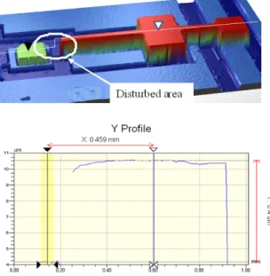
An example of cantilever profile is given in figure 2 after sacrificial layer etching and CO2 drying. The cantilever height is about 6µm instead of 5µm.
Figure 2. Optical profilometer measurement for a DC serie switch after release
The actuation voltage has been evaluated for several cantilevers between 12V and 15V and is consistent with the cantilever height. However, at 15 V, the force was not strong enough to ensure a high quality contact. Therefore 20V have been applied to insured the best contact performance. The losses have been measured and can be modeled with 1.1Ω contact resistance for each DC contact. In order to evaluate the contact force generated by the applied voltage, finite element calculations are
performed with CoventorWare [7]. The contact force is thus evaluated to 5µN for an applied voltage of 21V.
IV- methodology of contact analysis
The atomic force microscope is used to capture three dimensional data points of contact surfaces on the line and under the suspended beam. The figure 3 shows both 5x5µm² topographies. The AFM instrument stores 512 data points per scanned line and so the resolution step is equal to 9.8nm.
a b
Figure 3: AFM Roughness measurements on the signal line (a) and on the contact bump (b)
Then using Matlab functions we convert the closed surfaces from a stereolithographic format to an ANSCII file (figure 4) compatible with ANSYS Parametric Design Language (APDL). We can choose to keep the resolution step from the 3D capture or to filter the files in order to obtain larger steps of roughness definition.
The roughness on the bump is very low compared to the one on the line and we also neglect the thinner details on the membrane by defining a step of 220nm.
a b
Figure : Matlab treatment of both contact surfaces: line (a) and membrane (b)
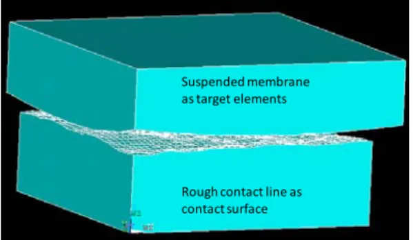
The rough surfaces are obtained in ANSYS by creating key points from the imported files. Since the key points are not coplanar, ANSYS uses Coons patches to generate the surfaces, and then we use a bottom up solid modeling to create the block volumes.
--- Suspended membrane as target elements Rough contact line as contact surface
Figure 5: flexible-to-flexible contact model built in ANSYS
The contact force is applied on the top surface of the membrane and we define some elastoplastic material properties for gold material (Table 1).
Table 1: gold material properties
Young Modulus E Poisson Ratio ν Yieldstress σ0 Tangent modulus Et
80000 MPa 0,42 300 MPa 10000 MPa
A first finite element analysis is run with a resolution step of the line roughness close to 117nm (figure 5). To perform the finite element contact analysis, we choose the combined method based on penalty and lagrangian methods called the augmented lagrangian method. The post processing generates the distribution of the contact pressure on the contact surface. The last version of ANSYS (version 11) presents an option allowing us to know directly the contact area on each element.
The figure 6 shows the distribution of the contact pressure on the contact surface of the line for an applied force equal to the generated contact force by the device.
Figure 6: distribution of the contact pressure on the rough contact line
One single contact spots appears on the contact surface with an equivalent radius of 33.3nm. This value is very close to the electron mean free path of gold (le~38nm). In this case, the electrical contact resistance is due to a quasi-ballistic transport of electron through the contact area [5].
When ballistic electron transport dominates, the formula of Sharvin’s resistance [2] is applied:
a
K
R
cBπ
ρ
3
4
=
wherea
l
K
=
eis the Knudsen number.
When diffusive electron transport dominates, the constriction resistance [1] is modeled analytically using:
a
R
cD2
ρ
=
Then Wexler [4] interpolates between the ballistic and diffusive electron transport regions:
cD cB
W
R
K
R
R
=
+
Γ
(
)
Where Γ(K) is a slowly varying Gamma function of unity order [3].
Finally we calculated Rc=0.49Ω.
The following step consists in defining locally the surface topography around the contact asperity. Our objective is to use the thinner step of resolution (9,8nm). This length is very small compared to the sample dimensions (5x5µm²) and thus we reduce also its dimensions to 1.5 x 1.5µm², by checking that these reductions don’t affect the mechanical contact results.
The contact analyses fail for the smaller steps (19.6 and 9.8nm) due to a too large number of degrees of freedom in the model. In order to reduce the number of elements, we choose to treat the suspended membrane as rigid and to define an equivalent contact material for the rough line. This model reduction implies some discrepancies on the mechanical results due to the elastoplastic properties of gold material.
--- Membrane rigide = plot de contact Ligne de contact rugueuse Rigid membrane as target elements Rough contact line as contact surface
Figure 7: rigid-to-flexible contact model built in ANSYS
V- Results and discussions
We present the results on the figure 8.
0 0,1 0,2 0,3 0,4 0,5 0,6 0,7 0,8 0,9 1 0 20 40 60 80 100 120 140 Co n ta ct r e si stanc e ( Ω ) discretization step (nm) flexible‐to‐flexible contact rigid‐to‐flexible contact
Figure 8: Contact resistance values as a function of the step of roughness definition for to contact
models
A smaller discretization step of roughness on the line (59nm) implies the emergence of three spots on the contact surface. Thus a smaller step allows the apparition of higher asperities. From a length of 20nm, the contact area is reduced to one single spot again but at another location than the initial spot. This case highlights the importance if thinner details of roughness in the contact model on the mechanical contact results.
In general, a lower step produces a smaller contact area and thus a larger contact resistance. With the limit length of 9,8nm, the value of the electrical resistance reaches 0.86Ω. The rigid-to-flexible contact model over-evaluates the contact area of about 30% for the 120, 60 and 40 nm steps. If we
take into account this consideration for the 10nm step, we obtained a contact resistance equal to 1.12Ω which is very close to the experimental measurements.
VI- Conclusions
The numerical tool succeeds to predict that a contact resistance of 1Ω can be obtained under actuation of the structure. This value is sufficiently low to guarantee good RF performances of the micro-switch. The experimental measurement performed on test structures allow to validate the novel numerical tool.
The method will be a very efficient tool for investigating the impact of materials, roughness, technological process end and the repeatability of the RF MEMS contact.
VII- References
[1] R. Holm, “Electric Contacts – Theory and Applications”, 4th ed. Berlin, Germany: Springer-Verlag, 1967.
[2] Y. V. Sharvin, Sov. Phys. JETP 21, 655 (1965).
[3] A. Mikrajuddin, F. Shi, H. Kim, K. Okuyama, “Size-dependant electrical constriction resistance for contacts of arbitrary size: from Sharvin to Holm limits”, in Proc. Mater. Sci. Sem., Vol. 2, 1999, pp. 321-327.
[4] G. Wexler, “the size effect and the nonlocal Boltzmann transport equation in orifice and disk geometry”, in Proc. Phys. Soc., Vol. 89, 1966, pp. 927-941.
[5] R.A. Coutu, J.R. Reid, R. Cortez, R.E. Strawser and P. Kladitis, “Microswitches with Sputtered Au, AuPd, Au-on-AuPt, and AuPtCu Alloy Electric Contacts”, IEEE transactions on Components and Packaging Technologies, vol. 29, No.2, June 2006.
[6] Oberhammer J 2004 Novel RF MEMS Switch and Packaging Concepts Ph.D. thesis, ISBN 91-7283-831-0, Stockholm 30, 31
[7] http://www.coventor.com
[8] K Yacine, F. Flourens, Biaxial initial stress
characterization of bilayer gold RF-switches,
European Symposium on Reliability of Electron Devices, Failure Physics and Analysis No16, vol. 45, no 9-11 (8 ref.), pp. 1776-1781,2005 [9] ANSYS: http://www.ansys.com/