HAL Id: hal-00485271
https://hal.archives-ouvertes.fr/hal-00485271
Submitted on 20 May 2010
HAL is a multi-disciplinary open access
archive for the deposit and dissemination of
sci-entific research documents, whether they are
pub-lished or not. The documents may come from
teaching and research institutions in France or
abroad, or from public or private research centers.
L’archive ouverte pluridisciplinaire HAL, est
destinée au dépôt et à la diffusion de documents
scientifiques de niveau recherche, publiés ou non,
émanant des établissements d’enseignement et de
recherche français ou étrangers, des laboratoires
publics ou privés.
InAs quantum wires on InP substrate for VCSEL
applications
Jean-Michel Lamy, Cyril Paranthoën, Christophe Levallois, Abdulhadi
Nakkar, Hervé Folliot, Olivier Dehaese, Alain Le Corre, Slimane Loualiche,
Olivier Castany, Laurent Dupont
To cite this version:
Jean-Michel Lamy, Cyril Paranthoën, Christophe Levallois, Abdulhadi Nakkar, Hervé Folliot, et al..
InAs quantum wires on InP substrate for VCSEL applications. Indium Phosphide & Related Materials
IPRM, 2008, Versailles, France. pp.1, �10.1109/ICIPRM.2008.4703028�. �hal-00485271�
InAs quantum wires on InP substrate for VCSEL applications
J. M Lamy, C. Paranthoen*, C. Levallois, A.
Nakkar, H. Folliot, O. Dehaese, A. Le Corre, S.
Loualiche
Laboratoire FOTON-INSA, UMR 6082
Rennes, France
* [email protected]
O. Castany, L. Dupont
Laboratoire FOTON-ENSTB, UMR 6082
Brest, France
Abstract—Quantum dash based vertical cavity
surface emitting lasers (VCSEL) on InP
substrate are presented. Single and close
stacking layers were successfully grown with
molecular beam epitaxy. Optimized quantum
dash layers exhibit a strong polarized 1.55 µm
photoluminescence
along
the
[1-10]
crystallographic axis. Continuous wave laser
emission is demonstrated at room temperature
for the first time on a quantum dash VCSEL
structure on InP susbtrate. The quantum dash
VCSEL laser polarization appears stable on the
whole sample and with excitation, no switching is
observed. Its polarization is mainly oriented
along [1-10], an extinction coefficient of 30 dB is
measured.
Those
preliminary
results
demonstrate the interests of quantum dashes in
the
realization
of
controlled
and
stable
polarization VCSEL devices
Keywords : quantum dashes, polarization, VCSEL, InP
I. INTRODUCTION
Vertical cavity surface emitting lasers (VCSEL) have been shown to be cost effective light sources for the optical network. They present the opportunity to benefit from an efficient coupling with optical fibers thanks to their circular beam, a spectral purity, and a high modulation bandwidth (typically 2-5 Gb/s) [1]. Because of this circular symmetry, the isotropic gain afforded by quantum wells (QWs) and the polarization independent reflectivity of Bragg mirrors, conventional QW VCSELs suffer from an optical output polarization instability, leading to an increase of the bit error data rates in optical telecommunication networks [2-3]. Several approaches have been conducted in order to control the VCSEL output polarization The use of a surface grating
mirror [4], an asymmetric cavity [5], an external polarized optical excitation [6], have shown improved performances. Apart technological tricks, previous work have shown that the use of an asymmetric gain within the active region may lead to a rather control of the VCSEL polarization,. Optical polarization extinction ratios (OPER) as high as 20-30 dB have been measured. This has been demonstrated using the growth of QWs on (311)B high index surface [7], or with the growth of quantum wires on a specific (775)B oriented substrate [8]. Recently, several groups have reported the growth of quantum wires like structures on InP substrate, presenting efficient performances in laser devices and semiconductor optical amplifier (SOA) [9], as well as some optical polarization anisotropy [10]. Because most industrially fabricated VCSEL are realized on (001) oriented substrate, we have focused on the realization of VCSEL devices based on quantum wires on InP(001), for applications in the telecommunication wavelength window.
In this paper, we present the growth on (001) oriented InP substrate of elongated InAs nanostructures, namely quantum dashes (QDHs), emitting at 1.55 µm, and presenting an important anisotropy in optical polarization. VCSEL structures based on QDHs have been realized and tested, continuous wave laser emission is demonstrated at room temperature for the first time at telecommunication wavelength with these nanostructures. The stability of the VCSEL polarization is discussed.
II. QDHS GROWTH AND OPTICAL CHARACTERIZATIONS
A. QDHs growth
Samples have been grown on (001) nominally oriented InP substrate, using gas-source molecular beam epitaxy. The nanostructures are spontaneously formed after the deposition at 480°C, of 2.1 InAs MLs on lattice matched Ga0.2In0.8As0.435P0.565 quaternary alloy. For optical characterizations, samples are capped following the double cap procedure, in order to control the wavelength emission. More details on double cap procedure can be found in previous papers [11].
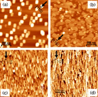
Figure 1. 1*1 µm² AFM images of a single layer of InAs nanostructures grown on InP(001) substrate with 13.4 (a), 1.5 (b), 0.3 (c) sccm AsH3 overpressure. (d)
is a 1*1 µm² AFM image of the sixth layer (0.3 sccm AsH3) of a QDHs
stacking sample with a 15 nm spacer layer thickness. Arrows indicate the [1-10] direction
Figure 1 (a), (b) and (c) represents 1*1 µm² Atomic force microscopy (AFM) images of samples grown after the deposition of 2.1 MLs of InAs with various AsH3 overpressure, from 13.4, 1.5 down to 0.3 sccm respectively. For the 13.4 sccm AsH3 flux, large islands with an average diameter of 60 nm are formed, with a 5.109 cm-2 density. The islands appear also to be slightly aligned along the [1-10] crystallographic axis, which corresponds to a favorable direction for diffusion of In adatoms. By decreasing the As overpressure, the aspect of the nanostructures change from big islands to small and elongated QDHs along the [1-10] crystallographic direction, mainly explained because of an increase of In adatom diffusion length,. In this last case, the linear density is measured to be close to 3.109 cm-1, height, width and typical length being respectively 2.5, 25 and 200-300 nm as measured by AFM.
In VCSEL structures, an important aspect is the optimization of the modal gain. It consists in the maximization of the active region material gain, and in increasing the overlapping between this region and the internal electric field of the cavity. Closely stacked of high density QDHs layers are thus required. Figure 1(d) represents the AFM image of the last QDH layer of a six QDH layers sample, separated with a 15 nm spacer layer thickness. This spacer layer thickness has been carefully reduced and optimized, in order to conserve the wire like morphology, without any degradation of photoluminescence intensity. Thanks to the strain induced mechanical coupling, a high QDH density is maintained (3.3 109 cm-1), close to the density of a single layer. Also, the length
of the QDHs slightly increases compared to a single layer, from 300 nm up to 500-700 nm.
B. Optical characterizations
Figure 2 presents the room temperature photoluminescence (RT PL) spectrum of a six QDH layers sample (15 nm spacer layer thickness). A polarizer has been inserted between the sample and the monochromator for polarization resolved measurements. The wavelength emission is well centred at 1.55 µm, the inhomogeneous broadening linewidth, related mainly to the QDHs height dispersion, is 130 nm. Compared with a single layer (not shown here), no significant degradation is observed in the PL linewidth and intensity.
Regarding the optical polarization properties of QDHs sample PL, the PL appears to be strongly polarized along the [1-10] direction, which corresponds to the elongated direction of the QDH structures. 1.2 1.3 1.4 1.5 1.6 1.7 1.8 0.00 0.05 0.10 0.15 0.20 0.25 0.30 0.35 25 . 0 I I I I PR ] 110 [ ] 0 1 1 [ ] 110 [ ] 0 1 1 [ = + − =
P
L
I
n
te
n
s
it
y
(
a
rb
.
u
n
it
s
)
λ
(µm)
polarizer along [1 1 0] polarizer along [1 1 0] 300KFigure 2. RT PL of a six QDHs layers sample, separated with a GaInAsP spacer layer of 15nm, as function of the polarizer orientation (collinear with [110] or [1-10] direction).
The polarization rate (PR) has been used for comparing the polarization of various samples. It is defined as follows: ] 110 [ ] 0 1 1 [ ] 110 [ ] 0 1 1 [
I
I
I
I
PR
+
−
=
(1)Where I[110] corresponds to the maximum intensity of the PL when the polarizer has been aligned along the [110] direction, and I[1-10] when the polarizer has been aligned along the [1-10] direction.
For a conventional structure based on seven lattice matched InGaAs quantum wells (QWs) on InP, we measured (not shown here) a low PR of 7 %. This difference in polarization properties of QWs has been explained to depend from As/P hetero-interface mixing [12]. On the QDH sample, we deduce
a significantly larger PR of 26 %. The origin of such important value may also come from As/P hetero-interface, but we believe the main factor should be the related to the morphology anisotropy of elongated QDH nanostructures.
III. VCSEL PROCESSING
VCSEL devices containing QWs or QDHs have been realized. The active region consists in three groups of 6 QDH layers (or InGaAs QWs lattice matched on InP), each group being located at a stationary electric field maximum intensity position of the microcavity. The microcavity has been designed with two dielectric Bragg mirrors, in order to benefit from a better reflectivity and thermal conductivity in comparison with epitaxial Bragg mirrors available on InP substrate [13]. The dielectric materials used are amorphous silicon and amorphous silicon nitride deposited with a magnetron sputtering system. The lower Bragg mirror of 6 periods is deposited directly on the sample. An Au-In eutectic bonding is employed to transfer the sample on a silicon substrate. The InP substrate is removed by mechanical polishing and chemical etching. The process ends up with the deposition of an upper Bragg mirror of 6 periods.
IV. VCSEL CHARACTERIZATIONS
A continuous wave (CW) YAG laser emitting at 1.064µm is used to optically pump the structure. The pump beam is focused on a circular spot of about 10µm. A Peltier cooler system is used to regulate the VCSEL temperature close to 15°C. 10 15 20 25 30 35 40 0 1 2 3 4 5 6 1.600 1.605 1.610 1.615 1.620 0.0000 0.0001 0.0002 0.0003 0.0004 0.0005 O u tp u t in te n s it y ( a rb . u n it .) Wavelength (µm)
O
u
tp
u
t
in
te
g
ra
te
d
i
n
te
n
s
it
y
(
a
rb
.
u
n
it
.)
Optical pump power (mW)
Figure 3 : Integrated intensity versus optical pump power (in continuous mode) of a 3*6 QDHs VCSEL. Insert is the spectrum (linear scale) recorded at a 30 mW pump power
Figure 3 is the integrated output intensity emitted from the QDH structure versus the pump power. Below an incident power of 27 mW, the integrated intensity is still rather low and linearly increases with the pump power. The spectrum is
centred close to 1.6 µm, and the linewidth is reduced compared to the PL peak, mainly because of microcavity effects. Above 27 mW, a fast increase of the output intensity is observed, as well as a reduction of the spectrum linewidth (inset of figure 3), corresponding to a laser emission. Although QDH structure is widely used in laser and SOA applications on InP substrate (see reference [9] and [10]), this report is the first demonstration of a CW VCSEL emission with QDHs at RT. For incident power larger than 32mW, the output intensity saturates and even starts to decrease, mainly because of thermal effects.
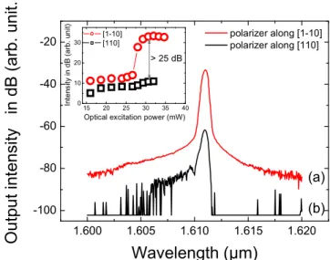
For polarization resolved measurements, an optical polarizer has been settled between the VCSEL and the spectrum analyser . Figure 4 represents the output laser spectra of the QDHs VCSEL, depending on the polarizer orientation. Above laser threshold, the QDH VCSEL emission is strongly polarized along the [1-10] direction. The OPER, defined as the ratio of the laser intensity polarized along [1-10] and the intensity polarized along [110], reaches a maximum value of 30 dB. On QW VCSELs, we measure a lower OPER of 5-20 dB. 1.600 1.605 1.610 1.615 1.620 -100 -80 -60 -40 -20 15 20 25 30 35 40 0 10 20 30 > 25 dB
Optical excitation power (mW)
In te n s it y i n d B ( a rb . u n it ) [1-10] [110] (a) polarizer along [1-10] polarizer along [110]
O
u
tp
u
t
in
te
n
s
it
y
i
n
d
B
(
a
rb
.
u
n
it
.)
Wavelength (µm)
(b)Figure 4 : RT CW laser emission spectra of a 3*6 QDHs VCSEL as function of the polarizer orientation ( (a) along [1-10], (b) along [110]), at an excitation power of 30 mW. Inset represents the VCSEL light output integrated intensity versus the optical excitation power, depending on the direction axis of the polarizer, along [110] (squares) and along [1-10] (circles)
The main difference between the QDH and QW VCSEL structures comes from the stability of the polarized laser emission. Indeed, as previously reported [2], the polarization of QWs VCSEL randomly switches from [110] to [1-10]. On the whole sample (1 cm²), we observed that the QWs VCSEL may be polarised along [110] or [1-10] in a random way. With the QDHs VCSEL, on the whole sample (1 cm²) the laser emission is still strongly polarized along [1-10], with an OPER varying from 20 to 30 dB. Also, on QWs VCSEL, we observed, as already reported (see reference [4]), that the device starts lasing on a certain polarization, and as the excitation increases the laser rapidly switches in polarization. Figure 4 inset represents the polarization
resolved output intensity versus pump power characteristics of the QDHs VCSEL, for the [110] and [1-10] direction. The device is mainly polarized along [1-10], and the output intensity polarization is still well established, and no switching is observed.
CONCLUSION
We have successfully grown QDH nanostructures and realized a QDH VCSEL emitting at the telecommunication wavelength. QDHs exhibit a strong polarized luminescence along the [1-10], corresponding to a polarization rate of 26%. A VCSEL device based on QDHs has been realised. CW lasing is demonstrated at RT, which consists in the first demonstration of a laser emission for a QDH VCSEL on InP substrate. This VCSEL exhibits a stable polarized laser emission on the whole sample without any switching, an OPER as high as 30 dB is measured. Those preliminary results which differ from conventional QW VCSEL, underline interests of QDH for the realization of a new type of fully control polarized emission VCSEL.
ACKNOWLEDGMENT
This project is supported by the National Agency of Research (ANR), through the project “λ-Access”.
REFERENCES
[1] M. B. Tayahi, S. Lanka, J. Wang, J. Catsten, L. Hofmann, and S. Sukanta, “High volume production of single mode VCSEL” Proc. SPIE, vol 6132, 613202, 2006.
[2] C. J. Chang-Hasnain, J. Harbison, L. T. Florez and N. G. Stoffel, “Polarization characteristics of quantum well vertical cavity surface emitting lasers”, Electron. Lett., vol 27, pp 163-165, 1991.
[3] H. Uenohara, K. Tateno, T. Kagawa, Y. Ohiso, H. Tsuda; T. Kurokawa and C. Amano, “Investigations of data transmission characteristics of polarisation-controlled 850 nm GaAs-based VCSELs grown on (311)B substrates”, Electron. Lett., vol 35, pp 45-46, 1999.
[4] J. M. Ostermann, P. Debernardi and R. Michalzik, “Surface grating VCSELs with dynamically stable output polarization”, IEEE Photon. Technol. Lett., vol 17, pp 2505-2057, 2005.
[5] K. D. Choquette and R. E. Leibenguth, “Control of vertical cavity laser operation with anisotropic transverse cavity geometries”, IEEE Photon. Technol. Lett., vol 6 , pp 40-42, 1994.
[6] S. Bandyopadhyay, Y. Hong, P. S. Spencer, and K. A. Shore, “VCSEL polarization control by optical injection”, J. Lightwave. Technol, vol 21, pp 2395-2404, 2003.
[7] Y.L. Okuno, J. Geske, K.G. Gan, Y.J. Chiu, S.P. DenBaars and J.E. Bowers, Appl. Phys. Lett,., vol 82, pp 2377-2379, 2003.
[8] Y. Ohno, S. Shimomura, S. Hiyamizu, Y. Takasuka, M. Ogura, K. Komori, “Polarization control of vertical cavity surface emitting laser structure by using self-organized quantum wires grown on (775)B oriented GaAs substrate by molecualr beam epitaxy”, J. Vac. Sci. Technol. B, vol 22, pp 1526-1528, 2004.
[9] J. P. Reithmaier, A. Somers, S. Deubert, R. Schwertberger, W. Kaiser, A. Forchel, M. Calligaro, P. Resneau, O. Parillaud, S. Bansropun, M. Krakowski, R. ALizin, D. Hadass, A. Bilenca, H. Dery, V. Milhelashvili, G. Eisenstein, M. Gioannini, I. Montrosset, T. W. Berg, M. van der Poel, J. Mork and B. Tromborg, “Inp based lasers and optical amplifiers with wire/dot like active regions”, J. Phys. D, vol 38, pp 2088-2102, 2005.
[10] Z. C. Lin, C. Y. Lu, C. P. Lee, “Self-assembled InAs quantum wires lasers”, Semicond. Sci. Technol., vol 21, pp 1221-1223, 2006. [11] C.Paranthoen, N.Bertru, O.Dehaese, A.Le Corre, S.Loualiche,
B.lambert, “Height dispersion control of InAs/Inp quantum dots emitting at 1.55µm”, Appl. Phys. Lett., vol 78, pp 1751-1753 ,2001.
[12] S. Cortez, O. Krebs, and P. Voisin, “In-plane optical anisotropy of quantum well structures: From fundamental considerations to interface characterization and optoelectronic engineering”, J. of Vac. Sci. Technol. B , vol 18, 2232-2234, 2000
[13] C. Levallois, A. Le Corre, S. Loualiche, O. Dehaese, H. Folliot, C. Paranthoen, F. Thoumyre, and C. Labbe, « Si wafer bonded of a-Si/a-SiNx distributed Bragg reflectorsfor 1.55-µm-wavelength vertical cavity surface emitting lasers”, J. Appl. Phys, vol 98, pp 43107, 2005.