HAL Id: hal-00789958
https://hal.inria.fr/hal-00789958
Submitted on 19 Feb 2013
HAL is a multi-disciplinary open access
archive for the deposit and dissemination of
sci-entific research documents, whether they are
pub-lished or not. The documents may come from
teaching and research institutions in France or
abroad, or from public or private research centers.
L’archive ouverte pluridisciplinaire HAL, est
destinée au dépôt et à la diffusion de documents
scientifiques de niveau recherche, publiés ou non,
émanant des établissements d’enseignement et de
recherche français ou étrangers, des laboratoires
publics ou privés.
Performance Upper Bound Analysis and Optimization of
SGEMM on Fermi and Kepler GPUs
Junjie Lai, André Seznec
To cite this version:
Junjie Lai, André Seznec. Performance Upper Bound Analysis and Optimization of SGEMM on Fermi
and Kepler GPUs. CGO ’13 - 2013 International Symposium on Code Generation and Optimization,
Feb 2013, Shenzhen, China. �hal-00789958�
Performance Upper Bound Analysis and Optimization
of SGEMM on Fermi and Kepler GPUs
Junjie Lai
INRIA, France [email protected]Andr´e Seznec
INRIA, France [email protected]Abstract
In this paper, we present an approach to estimate GPU ap-plications’ performance upper bound based on algorithm analysis and assembly code level benchmarking. As an example, we analyze the potential peak performance of SGEMM (Single-precision General Matrix Multiply) on Fermi (GF110) and Kepler (GK104) GPUs. We try to an-swer the question of how much optimization space is left for SGEMM and why. According to our analysis, the na-ture of Fermi (Kepler) instruction set and the limited issue throughput of the schedulers are the main limitation factors for SGEMM to approach the theoretical peak performance. The estimated upper-bound peak performance of SGEMM is around 82.5% of the theoretical peak performance on GTX580 Fermi GPU and 57.6% on GTX680 Kepler GPU. Guided by this analysis and using the native assembly lan-guage, on average, our SGEMM implementations achieve about 5% better performance than CUBLAS in CUDA 4.1 SDK for large matrices on GTX580. The achieved perfor-mance is around 90% of the estimated upbound per-formance of SGEMM on GTX580. On GTX680, the best performance we achieve is around 77.3% of the estimated performance upper bound. We also describe how to use na-tive assembly language directly in the CUDA runtime source code.
Categories and Subject Descriptors C.1.4 [Processor
Ar-chitectures]: Parallel Architectures; C.4 [Performance of Systems]: Modeling techniques; F.2.1 [Numerical Algo-rithms and Problems]: Computations on matrices
General Terms Measurement, Performance
Keywords Kepler GPU, Fermi GPU, SGEMM, CUDA,
Performance Upper Bound Analysis
Permission to make digital or hard copies of all or part of this work for personal or classroom use is granted without fee provided that copies are not made or distributed for profit or commercial advantage and that copies bear this notice and the full citation on the first page. To copy otherwise, to republish, to post on servers or to redistribute to lists, requires prior specific permission and/or a fee.
CGO 13 23-27 February 2013, Shenzhen China. 978-1-4673-5525-4/13/$31.00 c 2013 IEEE. . . $15.00
1.
Introduction
Nowadays, vendors are putting more and more comput-ing cores per die and the GPU architecture is evolvcomput-ing rapidly. Fermi and Kepler GPUs are the present genera-tions of NVIDIA GPUs [13, 14]. There are many studies about optimizing specific kernels on Fermi GPU. However, since the architecture is changing with each generation, we may need to repeat the optimization work again very soon. Unfortunately, no practical performance upper bound eval-uation is available to the developers. In practice, developers apply several optimization techniques based on the analysis to the algorithm or serial code, and their expert experience. Then developers may modify the optimizations with feed-back provided by tools like NVIDIA Visual Profiler [3]. However, they can not be sure how far the obtained per-formance is from the best achievable perper-formance. In this paper, we present an approach to project performance up-per bound using algorithm analysis and assembly code level benchmarking.
To understand GPU performance result, there exist many works about how to project/predict CUDA applications’ per-formance using analytical or simulation methods. Meng et al. [10] proposed a GPU performance projection framework based on annotated code skeletons. Hong and Kim [6] intro-duced the MWP-CWP model to predict CUDA application performance using PTX code. Bakhoda et al. [5] developed a detailed GPU simulator and the simulator also uses the PTX code as input. Recently, Sim et al. [17] extended the MWP-CWP model and utilize the assembly code of CUDA kernel to predict performance. The quantitative GPU performance model proposed by Zhang and Owens [20] is also based on the native assembly code. Since very little information about the underlying GPU architecture is disclosed, it be-comes very unlikely to build accurate simulators for each new GPU generation. Luckily, the results [6, 10, 17, 20] show that we can have very good approximation of GPU performance using analytical approaches. However existing GPU performance models all rely on certain level of an ap-plication’s implementation (C++ code, PTX code, assembly code. . . ) and do not answer the question of how good the current optimized version is and whether further
optimiza-tion effort is worthwhile or not. Different from existing GPU performance models, our approach does not project the pos-sible performance from certain implementations, but the per-formance upper bound that an application cannot exceed.
Researchers are also interested in the outcome of differ-ent optimization combinations on GPUs. The roofline model [19] is well known for estimating the optimization effects. The recent work by Sim et al.[17] studied the effects of dif-ferent optimization techniques on GPUs using the similar approach as the roofline model. However, the chosen opti-mizations normally rely on the initial code version and dif-ferent optimizations are likely to have complex impacts on each other. Our approach tackles the problem from the posite angle as the roofline method. We first assume an op-timistic situation on GPUs (no shared memory bank con-flict, global memory accesses are all coalesced, all the auxil-iary operations like address calculations are neglected, etc.). Then we try to predict a performance upper bound when mapping an application on the GPU based on the constraints introduced by the architecture, the instruction set and the application itself, or the constraints that we are not able to eliminate using optimization techniques. With a tight perfor-mance upper bound of an application, we have an evaluation on how much optimization space is left and can decide the optimization effort. Also, with the analysis, we can under-stand which parameters are critical to the performance and have more insights into the performance result. Hence, with these knowledge, it would be easier for the community to move to the new architecture.
As an example, we analyze the potential peak perfor-mance of SGEMM (Single-precision General Matrix Multi-ply) on Fermi (GF110) and Kepler (GK104) GPUs. GEMM
1operation is essential for Level 3 BLAS (Basic Linear
Al-gebra Subprograms) [2] routines and generally represents the practical best performance of a computer system. If we compare the performance of SGEMM from CUBLAS with the theoretical peak performance, on Fermi, it achieves around 70% and on Kepler, only around 42% of the theoreti-cal peak performance. There are already some articles about optimizing GEMM kernels on Fermi GPU [11] [18], and an auto-tuning framework has also been presented [7]. In this research, the focus is to answer the question of how much optimization space is left for SGEMM and why. We also show that the analysis can help optimization efforts since it uncovers critical parameters. Only single precision SGEMM is evaluated, since we could only access the GTX580 Fermi and the GTX680 Kepler Geforce cards, which have much poorer double precision performance than Tesla products. It is not really worth the effort to study the DGEMM per-formance on Geforce GPU. In November 2012, NVIDIA has announced the new Tesla K20X Kepler GPU (GK110) 1GEMM performs the matrix-matrix operation C := alpha ∗ op(A) ∗
op(B) + beta ∗ C. alpha and beta are scalars, and A, B and C are matrices. op(X) is op(X) = X or op(X) = XT.
and the documented SGEMM efficiency is around 73% of the theoretical peak performance [15]. The K20X Kepler GPU (GK110) architecture is different from the GTX680 (GK104) and uses a different instruction set (each thread can utilize maximum 255 registers on the new architecture while the limit is 63 on GTX680 GPU). With a Tesla GPU card, it should not be difficult to extend the analysis to SGEMM and DGEMM on the Tesla GPU using our approach.
This paper is organized as follows: Section 2 introduces our target GPU architectures. Section 3 introduces our as-sembly level benchmarking approach. Section 4 presents our analysis for performance upper bound of SGEMM on Fermi and Kepler GPUs. In Section 5 assembly code level opti-mization methods and performance result of SGEMM are presented. Section 6 concludes this study.
2.
GPU Architecture Characteristics
NVIDIA GPUs are composed of a cluster of independent SMs (Streaming Multiprocessor). Each SM includes sev-eral SPs (Streaming Processor), which is the basic comput-ing component, scheduler, SFUs (Special Functional Unit), LD/ST (Load/Store) Units, register file and a unified shared memory/L1 cache. The SPs inside one SM are similar to a lane of SIMD engines and they share the memory resource of the SM like the registers and shared memory.
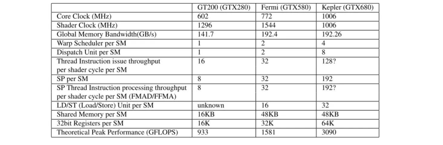
A comparison of the three generations of NVIDIA GPUs is illustrated in Table 1. From GT200 to Kepler GPU, the number of SPs increases dramatically, from 240 (GTX280, 65nm) to 1536 (GTX680, 28nm) [13, 14]. However, if we consider the memory resource (registers and shared mem-ory) per SP, the on-die storage per SP actually decreases. Previous generations have two clock domains in the SM, the core clock for the scheduler and the shader clock for the SPs. The shader clock is roughly twice the speed of the core clock. On Kepler (GK104) GPU, shader clock no longer ex-ists, the functional units with SMs run at the same core clock. However, to compare the different generations more easily, we still use the term shader clock on Kepler GPU. In the rest of this paper, all throughput data is calculated with the shader clock.
A typical CUDA [12] program normally creates thou-sands of threads to hide memory access latency or math pipeline latency. The threads are grouped into 1D to 3D blocks, and further into 1D or 2D grids. Each block is as-signed to one SM at execution time. The warp is the basic ex-ecution and scheduling unit of a SM, and is composed of 32 threads. We define a warp instruction as the same instruc-tion shared by all threads in the same warp, and a thread instruction as the instruction executed by one thread. So a
warp instruction launches 32 operations or consists of 32
thread instructions. On the SM, only a limited set of threads can run concurrently (active threads). On one hand, the in-creased SPs require more active threads to hide latency. On the other hand, the register and the shared memory resource
GT200 (GTX280) Fermi (GTX580) Kepler (GTX680) Core Clock (MHz) 602 772 1006
Shader Clock (MHz) 1296 1544 1006 Global Memory Bandwidth(GB/s) 141.7 192.4 192.26 Warp Scheduler per SM 1 2 4 Dispatch Unit per SM 1 2 8 Thread Instruction issue throughput 16 32 128? per shader cycle per SM
SP per SM 8 32 192
SP Thread Instruction processing throughput 8 32 192? per shader cycle per SM (FMAD/FFMA)
LD/ST (Load/Store) Unit per SM unknown 16 32 Shared Memory per SM 16KB 48KB 48KB 32bit Registers per SM 16K 32K 64K Theoretical Peak Performance (GFLOPS) 933 1581 3090
Table 1. Architecture Evolution limits the number of active threads. For the same
applica-tion, the active threads that one SP supports actually de-creases because of the reduced memory resource per SP from Fermi GPU to Kepler GPU. More instruction level parallelism within one thread needs to be explored (Section 4.3).
For Fermi (and Kepler GK104) instruction set, there is a hard limit of maximum 63 registers per thread (for GT200 generation the limit is 127 registers per thread) since in the instruction encoding, only 6 bits are left for one register.
3.
CUDA Programming with Native
Assembly Code
For performing this study, we have to develop some software components and reverse engineer many characteristics of the hardware. We use the GPU assembly code directly with an assembly tool Asfermi[1]. Asfermi was first developed to work on Fermi GPU. We patch Asfermi to support Kepler GPU (GK104) and manage to use native assembly language directly in the CUDA runtime source code.
3.1 Using Native Assembly Code in CUDA Runtime
API Source Code
Programming in assembly code on NVIDIA GPUs is not publicly supported by the company. However, our analysis is requiring such programming. With an assembly tool for Fermi GPU called Asfermi [1] and a little hacking into the CUDA programming compiling stages, we manage to use hand-tuned GPU assembly code in CUDA projects using CUDA runtime APIs .
There are several advantages of using assembly code or native machine code directly instead of using high level lan-guages like C++. First, we can carefully control the register allocation since the register resource per thread is very lim-ited and sometimes the compiler may spill many registers for programs utilizing much register resource per thread like SGEMM. Second, the instruction order can be carefully de-signed to better prefetch data from global memory and mix different instruction types to get better throughput. Third,
SIMD-like instructions (LDS.64 or LDS.128) could be used intentionally to reduce the instruction number. Also, we can control the exact behavior of the machine code. For exam-ple, the compiler might choose to use wider load instructions (LDS.64 or LDS.128) based on the data alignment in shared memory. However, using wide load instructions does not al-ways benefit the performance (Section 4.1).
3.2 Kepler GPU Binary File Format
Asfermi was first developed to work on Fermi GPU. We patched Asfermi to support CUDA sm 30 (GK104 Kepler GPU). However, although the CUDA program using assem-bly code kernel can still run correctly on Kepler GPU, the performance is very poor. The reason is that new control in-formation is embedded into the CUDA binary file to help processor scheduling. According to the GTX680 white paper [14], the compiler places the scheduling information along with the actual instructions in the CUDA binary file.
The scheduling information (we call it control notation) is placed before each group of 7 instructions and has the format of 0xXXXXXXX7 0x2XXXXXXX. 0x7 and 0x2 are iden-tifiers and the rest of the notation is separated into 7 fields and associated with each following instruction. It is similar to the explicit-dependence lookahead used in Tera computer system [4]. Unfortunately, NVIDIA does not disclose the en-coding of the control notation. We do not know how to gen-erate the control notation exactly as the nvcc compiler. In our implementation of SGEMM on Kepler GPU, as a com-promise, we use the same control notation for same kind of instructions and try to find the best combination of those no-tations for major instruction types. However, our decryption of the notations is still not enough.
3.3 Math Instruction Throughput on Kepler GPU
Understanding and modeling the behavior of math instruc-tions on Kepler GPU is a major difficulty. We use two ap-proaches to test the throughput of math instructions. First, a kernel is written in C++ code and compiled into binary with control notations embedded by nvcc. Second, a ker-nel is written in assembly code directly and the controlling
FADD R0, R1, R0 128.7 FADD R0, R1, R2 132.0 FADD R0, R1, R3 66.2 FMUL R0, R1, R0 129.0 FMUL R0, R1, R2 132.0 FMUL R0, R1, R3 66.2 FFMA R0, R1, R4, R0 129.0 FFMA R0, R1, R4, R5 132.0 FFMA R0, R1, R3, R5 66.2 FFMA R0, R1, R3, R9 44.2 IADD R0, R1, R0 128.7 IADD R0, R1, R2 132.4 IADD R0, R1, R3 66.2 IMUL R0, R1, R0 33.2 IMUL R0, R1, R2 33.2 IMUL R0, R1, R3 33.2 IMAD R0, R1, R4, R0 33.2 IMAD R0, R1, R4, R5 33.1 IMAD R0, R1, R3, R5 33.2 IMAD R0, R1, R3, R9 26.5
Table 2. Examples of Math Instruction Throughput on Ke-pler GPU with Various Operand Register Indices
notations are embedded with our parsing tool. Each thread executes the same 8192 math instructions. Each block has 1024 threads without synchronization and 40960 blocks are spawned to keep the GPU busy.
Instruction FFMA performs single precision fused multiply-add operation (FFMA RA, RB, RC, RD performs the
opera-tionRA := RB∗ RC + RD). With the first approach, the
instruction throughput of FFMA R9, R8, R9, R5 is measured as 129.2 operations per shader cycle2. With the second ap-proach and the control notation of 0x25, the throughput is 132.0 operations per shader cycle (The actual shader clock cannot be obtained during execution. All throughput data is calculated by boost clock of 1058MHz[14]).
Some math instructions’ throughput is illustrated in Ta-ble 2 measured with the second approach. In these cases, the scheduling function units on one SM can only issue about maximum 132 thread instructions per shader cycle, which is much lower than the SP’s processing throughput (192 thread instructions per shader cycle). If some of the three source registers are the same (like FFMA RA, RB, RB, RA), with some carefully designed code structures, the FFMA throughput can approach around 178 thread in-structions per shader cycle. However, considering ’useful’ FFMA’s throughput, that is (FFMA RA, RB, RC, RA), the maximum single precision performance for many applica-tions like SGEMM on GTX680 GPU (GK104) cannot ex-ceed around 68.75% (132/192) of the claimed performance (3090GFlops) by NVIDIA.
Our benchmark result also shows that the instruction throughput is related to register indices. According to some other experiments, we speculate that the registers reside on four banks. Take the instruction FFMA RA, RB, RC, RD for instance, if there are two different source registers on the same bank, the throughput drops by 50%, and if all three source registers RB, RC, RD are different registers on the same bank, the throughput is around 33.3% of the best 2The actual implementation is not 8192 FFMA R9, R8, R9, R5 instructions
per thread but 4 independent FFMA instructions like FFMA R9, R8, R9, R5 unrolled by 2048 times. Shared Memory L L L L � TB∗ BR � TB∗ BR Prefetch Prefetch A C B
Figure 1. SGEMM Implementation
case. We name the four banks as even 0 (Rindex%8 < 4
&& Rindex%2 == 0), even 1 (Rindex%8 ≥ 4 &&
Rindex%2 == 0), odd 0 (Rindex%8< 4 && Rindex%2 ==
1), and odd 1(Rindex%8≥ 4 && Rindex%2 == 1). Since
we implement SGEMM with assembly code directly, the register indices have to be carefully chosen to make sure there is no bank conflict. The detailed optimization is illus-trated in section 5.4.
4.
Analysis of Potential Peak Performance of
SGEMM
The general analysis approach can be similar for all appli-cations while the detailed analysis process may differ from application to application. Our method is applicable for ap-plications which use a few major instruction types and a sim-ple execution path. Many high-performance computing ker-nels have this characteristic, especially linear algebra rou-tines. Our analysis requires characteristics of the architec-ture such as register file size, maximum number of registers per thread, shared memory size, instruction throughput for different instruction mix, etc. Those characteristics need to be collected on the real hardware and are independent of the effective application.
First, we should analyze the instruction types and per-centage of a routine. Second, we should find the critical parameters which affect the different instructions’ mixing percentage. Third, we analyze how the instruction through-put changes when we vary these critical parameters. Fourth, we can use the instruction throughput with critical parame-ters’ optimal combination to estimate the performance up-per bound. With this approach, not only we can have the performance upper bound estimation, know how much per-formance gap is left and decide the optimization effort, but we can also understand what parameters are essential to the performance and how to distribute our optimization effort.
For SGEMM, all well-implemented SGEMM kernels actually utilize shared memory on the GPU to reduce the global memory pressure as illustrated in Figure 1. First, data is loaded from global memory to shared memory and then threads within one block can share the loaded
data in the shared memory. For Fermi (GF110) and Kepler (GK104) GPUs, arithmetic instructions like FFMA cannot take operands from the shared memory. Since LDS instruc-tions are needed to load data first from shared memory into registers, most of the instructions executed in SGEMM are FFMA and LDS instructions. For instance, in our SGEMM implementation with 1024x1024 matrix size, 80.5% of in-structions executed are FFMA inin-structions and 13.4% are LDS.64 instructions. So essentially, in our analysis, we de-fine a few key parameters and study the instruction through-put mixing FFMA and LDS.X instructions while varying these parameters.
The rest of this section is our analysis of SGEMM’s performance upper bound. We show that the analysis can give good insights about how to optimize a specific kernel (SGEMM) and help us to understand the performance result.
4.1 Using Wider Load Instructions
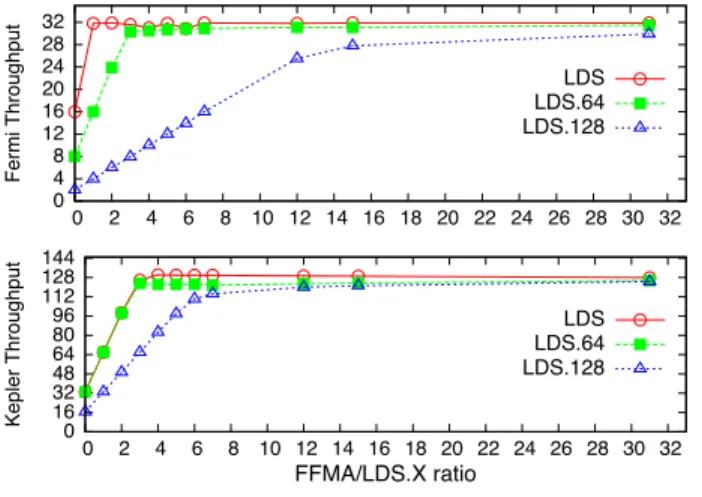
To achieve better performance, it is essential to minimize auxiliary instructions’ percentage. By auxiliary instructions, we mean non-math instructions, especially LDS instruc-tion. The assembly code for CUDA sm 20 (GF110 Fermi GPU) and sm 30 (GK104 Kepler GPU) provides SIMD-like LDS.64 and LDS.128 instructions to load 64bit and 128bit data from the shared memory. Using wider load instructions can reduce the total number of LDS instructions.
According to our benchmarks, on Fermi GPU, the peak throughput for LDS instruction is 16 32bit-operations per shader clock per SM. Using LDS.64 instructions does not increase the data throughput and the LDS.128 instruction normally leads to 2-way shared memory bank conflict on Fermi GPU. LDS.128 has the throughput of only 2 thread instructions per shader cycle on one SM. On Kepler GPU, the throughput for LDS operation is measured as 33.1 64bit operations per shader clock per SM. Using the 32bit LDS operation actually decreases the data throughput in half com-paring with using LDS.64 instructions and properly used LDS.128 instruction does not introduce penalty.
0 4 8 12 16 20 24 28 32 0 2 4 6 8 10 12 14 16 18 20 22 24 26 28 30 32 Fermi Throughput LDS LDS.64 LDS.128 0 16 32 48 64 80 96 112 128 144 0 2 4 6 8 10 12 14 16 18 20 22 24 26 28 30 32 Kepler Throughput FFMA/LDS.X ratio LDS LDS.64 LDS.128
Figure 2. Thread Instruction Throughput Mixing FFMA and LDS.X
Figure 2 illustrates the instruction throughput of mixing FFMA and LDS.X instructions. While gradually increasing the ratio of FFMA instructions to LDS instructions, the over-all instruction throughput approaches the FFMA’s peak pro-cessing throughput. The instruction ratio of FFMA to LDS.X depends on the algorithm parameters such as register block-ing size. Apparently, the overall performance does not al-ways benefit from using wider load instructions. However, the compiler might choose to use the wider load instructions based on the data alignment in the shared memory. With the native assembly language, it is possible for us to carefully design the data layout and use the best instruction type.
4.2 Register Blocking
As in Table 1, the scheduler of GT200 GPU can issue one warp instruction like FFMA per core cycle and since there are 8 SPs per SM, SPs need 4 shader cycles to process one warp instruction. Apparently, as the issue throughput is higher than the SP’s processing throughput, math instruc-tions executed in SPs cannot saturate the scheduler’s issue throughput. So the scheduler has some ’free cycles’ to issue instructions to other functional units.
On Fermi GPUs, SM are redesigned with 2 warp sched-ulers and 32 SPs. Each warp scheduler, equipped with one dispatch unit, issues instructions to 16 SPs. With an issue rate of one warp instruction per shader cycle, the schedulers’ ability could be fully utilized by 32 SPs. The theoretical peak performance for math instructions comes from the SPs’ per-formance. The percentage of other instructions becomes an issue when there are many auxiliary instructions: there are fewer cycles left for schedulers to issue useful instructions like FFMA. 0% 20% 40% 60% 80% 100% 2 4 6 8 10 12 14 0% 10% 20% 30% 40% 50% 60% 70% 80% 90% 100%
FFMA Instruction Percentage
Register Blocking Factor
75% 85.7% 92.3% LDS LDS.64 LDS.128
Figure 3. FFMA Instruction Percentage in SGEMM Main-loop with Different Register Blocking Factors
In the worst case, without any register reuse, 2 LDS in-structions are needed to fetch data for 1 FFMA instruction in the SGEMM main loop. In that case, only 1/3 of the instruc-tions are floating point operainstruc-tions. Blocking is a well-known technique to better utilize memory hierarchy for scientific programs [8, 9]. To increase the percentage of math instruc-tions, register blocking is needed. We illustrate the
percent-age of FFMA instructions varying register blocking factors in Figure 3.
If 6-register blocking is used (which is the case of our SGEMM implementation on Fermi GPU), the FF-MA/LDS.X ratios are 3:1, 6:1, and 12:1 if shared memory accesses are implemented with LDS, LDS.64 and LDS.128 respectively. The percentage of FFMA instructions is 75%, 85.7% and 92.3%. On Fermi GPU, the overall instruction throughputs for one SM in these cases are 31.3, 30.4 and 24.5 thread instructions per shader clock. Because using LDS.128 instruction may lead to extra penalties, even if all the accesses to shared memory are implemented with LDS.128, in the best case we can only achieve around 71% (24.532 ∗ 92.3%) of SMs’ single precision floating point per-formance. Also, in many cases, a lot of padding in shared memory has to be used to get proper data alignment. Appar-ently, it is not worth the programming effort to mix FFMA with LDS.128 for SGEMM on the Fermi GPU.
4.3 Active Threads on SM
Normally, the more active threads one SM executes, the higher performance the GPU can achieve. Since register and shared memory resource is limited per SM, only a limited set of warps can be executed concurrently (TSM).
TSM∗ RT ≤ RSM (1)
The registers that each thread can utilize (RT) is less
than or equal to 63 on Fermi and Kepler GPUs (RM ax).
Furthermore, the register budget of the active warps cannot exceed the SM’s register amount (RSM) (Equation 1).
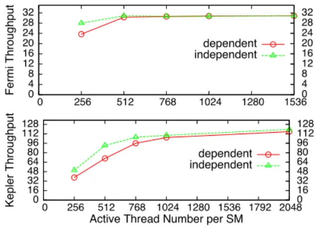
0 4 8 12 16 20 24 28 32 0 256 512 768 1024 1280 1536 0 4 8 12 16 20 24 28 32 Fermi Throughput dependent independent 0 16 32 48 64 80 96 112 128 0 256 512 768 1024 1280 1536 1792 2048 0 16 32 48 64 80 96 112 128 Kepler Throughput
Active Thread Number per SM dependent independent
Figure 4. Instruction Throughput Mixing FFMA and LDS.64 with Ratio of 6:1
Figure 4 illustrates the instruction throughput mixing FFMA and LDS.64 instructions with ratio 6:1 under dif-ferent number of active threads on one SM. We tested two cases. In the first case ( ’independent’ in Figure 4), 6 FFMA and 1 LDS.64 instructions are all independent. In the second case ( ’dependent’ in Figure 4), 6 FFMA instructions are dependent on one LDS.64 instruction. The second case is closer to the actual implementation of SGEMM. On Fermi
GPU, with 512 active threads, the instruction throughput of the second case is already close to the best situation. On Ke-pler GPU, however, with fewer than 1024 active threads, the Kepler GPU is very sensitive to the dependences between instructions.
4.4 Register and Shared Memory Blocking Factors
Larger register blocking size can introduce more register reuse within one thread and higher percentage of FFMA instructions. However, the register blocking size is limited by the register resource on the SM and the instruction set constraint. With a register blocking factorBR, if we only
consider the registers needed for blocking, we can describe the resource constraint as Equation 2.
BR2 + BR+ 1 < RT ≤ RM ax (2) This loose condition for register blocking factorBRcan
be used to roughly estimateBR.BR2 is the register set needed
to hold C sub-matrix per thread,BR is one column/row of
A or B sub-matrix. For instance, with maximum 63 registers per thread,BR≤ 7.
As depicted in Figure 1, TB ∗ BR2 is the size of the
C sub-matrix per block (each block has TB threads) and
p
TB∗ BR2 ∗ L is the size of a sub-matrix for A or B (L is
the stride). To overlap the data transfer and the computation, extra registers are needed to fetch data from global memory to shared memory since no direct data transfer is provided
between the two memory space. The strideL needs to be
chosen such that each thread loads the same amount of data (Equation 3).
(√TB∗ BR∗ L)%TB= 0 (3)
Considering data prefetching from global memory and a few registers to store the addresses of matrices in global memory and shared memory (Raddr), the overall strict
con-straint for register blocking factor can be described as Equa-tion 4.
BR2+
2 ∗√TB∗ BR∗ L TB
+BR+1+Raddr≤ RT ≤ RM ax (4) Since shared memory is allocated in block granularity, forBlk active blocks, Blk∗ 2 ∗√TB∗ BR∗ L is needed
to store prefetched global memory data (Equation 5). The
shared memory blocking factor can be defined asBSh =
p
TB∗ BR2. With the shared memory blocking factorBSh,
the performance bounded by global memory bandwidth can be roughly estimated using Equation 6.
Blk ∗ 2 ∗√TB∗ BR∗ L ≤ ShSM (5) PM emBound #GlobalM em bandwidth = 2 ∗ BSh2 2 ∗ BSh∗ 4 (6)
4.5 Potential Peak Performance of SGEMM
The instruction factorFI is the ratio of FFMA instructions
LDS.X instructions here). It depends on the choice of LDS.X instruction and register blocking factorBR (Figure 3). For
instance, if LDS.64 is used with register blocking factor 6, FI = 0.5.
The throughput factorFT is a function of register
block-ing factor (BR), number of active threads (TSM), throughput
of SPs (#SP T P), LD/ST units (#LDS T P) and dispatch
units (#Issue T P)) (Equation 7). The functionf for Fermi and Kepler GPUs is illustrated in Figure 2 and in Figure 4 (only shows LDS.64) and obtained through benchmarks varying these parameters.
FT = f (BR, #Issue T P, #SP T P, #LDS T P, TSM) (7) With the register blocking factor BR, the instruction
factor FI and the throughput factor FT, the performance
bounded by SMs’ processing throughput is estimated as Equation 8 and the overall performance is as Equation 9.
PSM Bound=
BR2 B2
R+ BR∗ 2 ∗ FI
∗ FT∗ Ptheoretical (8) Ppotential= min(PM emBound, PSM Bound) (9) With the previous analysis, we can estimate the perfor-mance upper bound of SGEMM on Fermi and Kepler GPUs. On the Fermi GPU for instance, because of the hard limit of 63 registers (RM ax) per thread, considering prefetching and
using the strict condition of Equation 4, the maximum block-ing factor is only 6. The detailed register allocation is illus-trated in Section 5.2. With the register blocking factor of 6, the register resource per SM can support up to 512 threads. Using Equation 3, we choose 256 threads per block.
To easily program the data prefetching, according to Equation 3, L could be 8, 16, 24, . . . . Considering the con-dition in Equation 4, we choose L as 16. With a 6-register blocking factor, mixing LDS or LDS.64 with FFMA in-structions, the throughput can achieve close to 32 thread instructions per shader clock per SM. Using a LDS.64 in-struction can increase the FFMA inin-struction percentage to 85.7% from 75% (using LDS). Though LDS.128 instruction can provide higher percentage of FFMA instructions, the instruction processing throughput is too low.
According to Equations 6, 8 and 9, the performance is bounded by SMs’ processing throughput, and the potential peak is about 82.5% (62+6∗2∗0.562 ∗
30.8
32 ) of the theoretical
peak performance for SGEMM. The main limitation comes from the nature of the Fermi instruction set and the limited issue throughput of schedulers.
It is similar to estimate the performance upper bound of SGEMM on Kepler GPU as Fermi GPU. The Kepler GPU (GK104) instruction set is very close to that of Fermi GPU. It means that the limit of 63 registers per thread still exists. Thus, 6-register blocking is also applicable. And the register resource can support 1024 active threads per SM (64K 32bit registers per SM). We can choose either 256 or 1024 threads per block. Similarly, if we use LDS.64 instructions, the FFMA instruction percentage is 85.7%. If
we use LDS.128 instructions (need padding or data layout transform), the FFMA instruction percentage is 92.3%.
Similarly, according to Equations 6, 8 and 9, the perfor-mance is bounded by SM’s processing throughput, and the potential peak is about 54.6% (62+6∗2∗0.562 ∗
122.4 192 ) of the
theoretical peak performance for SGEMM using LDS.64 in-structions. Using LDS.128 instructions, the potential peak is about 57.6% (62+6∗2∗0.2562 ∗
119.9
192 ) of the theoretical peak.
The main limitation factors are still the nature of instruction set and the limited issue throughput of schedulers.
5.
Assembly Code Level Optimization
The estimated performance upper bound is a limit that an actual implementation cannot exceed. It can be a little opti-mistic since we only consider the major performance degra-dation factors. Besides the considered parameters, there might be other aspects which can limit the performance. The ’real’ upper bound or the best possible performance is between the estimated upper bound and the achieved perfor-mance.
Depending on whether to apply transpose operation on in-put matrix A or B, there are 4 variations for GEMM kernel. Figure 5 illustrates the performance of four SGEMM vari-ations from CUBLAS and our implementation (ASM) with 2400x2400 and 4800x4800 matrices. On GTX580 GPU, we achieve around 74.2% of the theoretical peak performance, i.e., about 90% of the estimated performance upper bound, which we think is good enough. In our analysis, we only study the two main instruction types. There are other auxil-iary instructions which do not devote to the GFLOPS. And also, we do not consider the effect of barriers which will harm the performance too. We show that the ’real’ upper bound is within this 10% and future optimization is unlikely to achieve a lot of speedup. On Kepler GPU, although we cannot provide the optimal controlling information as dis-cussed in section 3.2, we achieve around 77.3% of the esti-mated upper bound. Similar to Fermi GPU, there are some factors we do not consider in our analysis. The larger gap between our achieved performance might be due to our very limited knowledge of the undisclosed scheduling informa-tion of Kepler GPU, which is critical to performance or to some hidden characteristics that we are not able to dis-cover due to limited documentation. Figure 6 illustrates the performance comparison on Fermi GPU between our im-plementation (assembly), CUBLAS from CUDA 4.1 and MAGMA library [11]. Figure 7 is the performance compari-son on Kepler GPU between our implementation (assembly), CUBLAS from CUDA 4.2 and MAGMA library.
The rest of the section briefly describes our optimizations on assembly code level of SGEMM.
5.1 Optimization of Memory Accesses
Assembly code level optimization of memory accesses is similar to high level language optimization. Global memory
700 800 900 1000 1100 1200 1300 1400 1500
Fermi_2400Fermi_4800Kepler_2400Kepler_4800
GFLOPS
CUBLAS ASM
Figure 5. SGEMM Performance of CUBLAS and Our Im-plementation on Fermi and Kepler GPUs
400 600 800 1000 1200 500 1000 1500 2000 2500 3000 3500 4000 4500 400 500 600 700 800 900 1000 1100 1200 G Flops Matrix Size assembly cublas_4.1 magma_sgemm_fermi
Figure 6. SGEMM NN Performance on GTX580
400 600 800 1000 1200 1400 500 1000 1500 2000 2500 3000 3500 4000 4500 400 500 600 700 800 900 1000 1100 1200 1300 1400 G Flops Matrix Size assembly cublas_4.2 magma_sgemm_fermi
Figure 7. SGEMM NN Performance on GTX680 requests from the threads within a warp could be grouped (coalesced) into one or more memory transactions depend-ing on the compute capability of the device and the memory accessing pattern. To access global memory efficiently, gen-erally it is better to let threads in a warp access continuous data elements in global memory to get coalescing. Consid-ering the majority of instructions in the SGEMM main loop are FFMA and LDS, and it is critical to reduce the number of LDS instructions (using LDS.64 or LDS.128), sub-matrices in shared memory should be grouped such that each thread accesses continuousBRdata elements. Also, proper padding
needs to be applied to reduce shared memory access conflicts and satisfy the alignment restriction of the LDS instruction.
5.2 Register Spilling Elimination
The register resource is 32K 32-bit registers per SM for the Fermi GPU and each thread can use a maximum of 63 registers. The register R1 is normally occupied as stack pointer. According to our analysis, the number of per-thread registers with prefetching is at leastB2
R+
2∗√TB∗BR∗L
TB +
BR+ 1 +Rindex. With the register blocking factor of 6 for
Fermi GPU, the register allocation of our implementation is
as the following. Note that we use 32bit addressing to save address registers.
1.B2
R, 36 registers to save intermediate result for C matrix.
2. 2∗
√
TB∗BR∗L
TB , 12 registers to prefecth A and B from
global memory.
3.BR+ 2, 6 registers to load A from shared memory and
2 registers to load B from shared memory during the main loop. Using 2 registers for B is because LDS.64 instruction is used.
4. 2 registers. Track of A, B in global memory during the prefetching.
5. 1 register to store the loop end condition.
6. 2 registers. Track of A, B in shared memory during the prefetching.
7. 2 registers. Track of A, B in shared memory in the main loop.
In all, 63 registers are used. Since we do not need thread stack, R1 is used to store the loop end condition in our code. Therefore, we are able to fully eliminate the register spilling.
5.3 Instruction Reordering
Generally, we try to interleave different instruction types to get better balance between functional units within one SM and better instruction throughput. We apply the following simple reordering optimizations:
1. In the main loop, between the 2 barriers are all shared memory accesses. By moving address calculation from start of the loop to mix with the shared memory accesses, we can achieve better performance.
2. Interleaving prefetching from global memory with FFMA and LDS instructions can benefit performance.
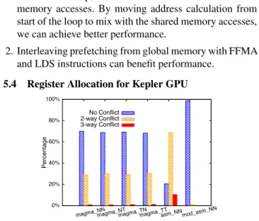
5.4 Register Allocation for Kepler GPU
0% 20% 40% 60% 80% 100%
magma_NNmagma_NTmagma_TNmagma_TTasm_NNmod_asm_NN
Percentage
No Conflict 2-way Conflict 3-way Conflict
Figure 8. Register Conflict of FFMA Instruction As we describe in Section 3.3, to get the best throughput, the 3 source registers of FFMA instructions should reside on 3 different banks if they are different. In our current implementation, 6-register blocking is used. 6 registers are used to load A from the shared memory and 2 registers to load B from the shared memory in the main loop. 36 different registers (R26∼R61) hold the C sub-matrix. In this implementation, register spilling is eliminated.
R6 R7 R27 R28 R33 R30 R35 R36 R29 R26 R31 R32 R37 R34 R41 R38 R43 R44 R49 R46 R39 R40 R45 R42 R47 R48 R51 R52 R57 R54 R59 R60 R53 R50 R55 R56 R61 R58 R8 R9 R10 R11 R18 R19 E1 O1 E1 O1 E1 O1 O E1/ O0 O E1/ O0 O E1/ O0 O1 /E0 E O1 /E0 E O1 /E0 E O E1/O0 O E1/O0 O E1/O0 O1 /E0 E O1 /E0 E O1 /E0 E O E1/O0 O E1/O0 O E1/O0 O1 /E0 E O1 /E0 E O1 /E0 E E0 O0 E0 O0 E0 O0 A C B Col A Row B Sub-matrix C Register Allocation
Constraints Final Register Mapping
R6 R7 R6 R7
Figure 9. Register Allocation As in Figure 8, around 30% of the FFMA instructions
in the MAGMA [11] SGEMM binary for the Kepler GPU (nvcc generated) have the 2-way register bank conflict and 1% of the FFMA instructions have the 3-way register bank conflict. In our first version of SGEMM NN on GTX680, which achieves around 1100GFLOPS, 68.8% of the FFMA instructions have the 2-way register bank conflict, and 10.6% of the 3-way conflict. After applying the optimization, the modified version, which achieve around 1300GFLOPS, has only 1.2% of the 2-way FFMA register bank conflict and the 3-way conflict is fully removed.
Our optimization is depicted in Figure 9. In the SGEMM main loop, at each stage, one column from matrix A and one row from matrix B are processed. To use the register block-ing and the LDS.64 instructions, at least 6 and 2 different registers are needed for column A and row B. Of course, there are many possible implementations, here we describe one possibility. We select registers from E0 and O0 for col-umn A. Row B uses registers from E1 and O1. Then we use the first table in Figure 9 as the constraints of register allo-cation. In the final mapping stage, we make sure that 36 reg-isters of C sub-matrix have 9 regreg-isters on each bank and had our register allocation as the second table, which does not have any register bank conflict to compute the 36 elements from the C sub-matrix.
5.5 Opportunity for Automatic Tools
Our study emphasizes that for Fermi and Kepler GPUs, it is essential to study the impact of algorithm parameters on instruction throughput to get insight into the performance result. The main optimization opportunity comes from the allocation of registers. For example, the four SGEMM vari-ations of MAGMA library compiled with nvcc spill at least 10 registers (40 Bytes) on the Kepler GPU. When the active thread number is 512, at least 20KB L1 cache is needed to make sure that the spilled data stays in the L1 cache. How-ever, since normally the unified 64KB shared memory/L1 cache is configured as 48KB shared memory and 16KB L1 cache, some data will be spilled out of L1 cache. As the ac-tive threads increase, more data is spilled out of L1 cache and the performance will be harmed. We already show that with
careful design, register spilling could be eliminated. We also show that around 30% of FFMA instructions in the nvcc-generated SGEMM binary from MAGMA library have reg-ister bank conflict. We propos a simple solution in Section 5.4. It is possible for optimizers to detect the loop structure and remove the conflicts with proper register allocation.
An automatic tuning tool normally needs to explore a large design space and evaluate the performance of many configurations [7, 10, 16]. It may take a significant amount of time. Normally, the automatic tuning tool is application-dependent and each includes several efficient optimizations for the specific application. To build the tool relies on the de-velopers’ understanding of the application and optimization experience. With the proposed analysis approach, we can better understand which parameters are critical to the per-formance. The estimated upper bound actually corresponds to a set of parameters and optimization options. This knowl-edge can help an automatic tool to explore the design space in a relatively small region. And of course by comparing the performance of an automatic tool’s output code and the esti-mated performance upper bound, we can judge whether the optimized version is good enough.
In our analysis, to study the instruction throughput mix-ing FFMA and LDS.X instructions, we manually write some benchmarks varying several key parameters such as instruc-tion type choice (LDS.X), the mixing ratio, the blocking fac-tor, the instructions’ dependence, active threads and study these parameters’ impact on the instruction throughput. For many applications with few major instruction types, a sim-ilar approach can be used to estimate the performance up-per bound. The difference would be the chosen instruction types and their mixing pattern (mixing ratio, dependence, etc.). Systematic and automatic development of a set of mi-crobenchmarks to help to estimate the performance upper bound of other applications is possible. A family of assem-bly level microbenchmarks could be defined and evaluated in order to provide a small database of performance refer-ences that could be used by the auto-tuning tool, and also the developer to transform the code for performance. Generally, the assembly level microbenchmarks can also help to
un-derstand the difference between different GPU architectures. For example, the benchmarks illustrated in Figure 4 show the increasing need for active threads on Kepler GPU. As-sembly level benchmarking requires an asAs-sembly tool chain which is missing from the official support. We manage to make it work on Fermi GPU. But on Kepler, there are some issues like the hidden scheduling information, which we can-not fully decrypt.
6.
Conclusion
In this work, we have proposed an approach to analyze GPU applications’ performance upper bound. Different from ex-isting works on GPU performance models, our approach re-lies on application analysis and assembly level benchmark-ing. As an example, we analyze the potential peak perfor-mance of SGEMM on Fermi and Kepler GPUs. We show that the nature of the Fermi (Kepler) instruction set and the limited issue throughput of schedulers are the main limita-tion factors for SGEMM to approach the theoretical peak performance. The general guideline is to reduce the auxil-iary instructions and increase the FFMA instruction’s per-centage. Proper register allocation, shared memory data lay-out and memory access pattern need to be carefully designed to minimize the impact of memory accesses on performance. We also show that our analysis can help to decide some crit-ical algorithm parameters and show how much optimization space exists. Guided by the analysis, we further optimize the four SGEMM kernel variations and achieve better perfor-mance on Fermi GPU (around 5% on average for large ma-trices) than highly optimized routine provided by NVIDIA.
7.
Acknowledgments
Many thanks to CJ Newburn, our shepherd and the anony-mous reviewers for their insightful comments on improving this paper. This work is supported by French National Re-search Agency (ANR) through COSINUS program (project
PETAQCD NoANR-08-COSI-010).
References
[1] Asfermi. http://code.google.com/p/asfermi/. [2] Netlib. http://www.netlib.org/blas/.
[3] Nvidia. Visual Profiler, https://developer.nvidia. com/nvidia-visual-profiler.
[4] R. Alverson, D. Callahan, D. Cummings, B. Koblenz, A. Porterfield, and B. Smith. The tera computer system. In Proceedings of the 4th international conference on Supercom-puting, ICS ’90, New York, NY, USA, 1990. ACM.
[5] A. Bakhoda, G. Yuan, W. Fung, H. Wong, and T. Aamodt. Analyzing cuda workloads using a detailed gpu simulator. In Performance Analysis of Systems and Software, 2009. ISPASS 2009. IEEE International Symposium on, april 2009. [6] S. Hong and H. Kim. An analytical model for a gpu
architec-ture with memory-level and thread-level parallelism aware-ness. In Proceedings of the 36th annual international
sym-posium on Computer architecture, ISCA ’09, New York, NY, USA, 2009. ACM.
[7] J. Kurzak, S. Tomov, and J. Dongarra. Autotuning gemm kernels for the fermi gpu. Parallel and Distributed Systems, IEEE Transactions on, PP(99):1, 2012.
[8] M. D. Lam, E. E. Rothberg, and M. E. Wolf. The cache per-formance and optimizations of blocked algorithms. SIGPLAN Not., 26(4):63–74, Apr. 1991.
[9] A. C. McKellar and E. G. Coffman, Jr. Organizing matrices and matrix operations for paged memory systems. Commun. ACM, 12(3):153–165, Mar. 1969.
[10] J. Meng, V. A. Morozov, K. Kumaran, V. Vishwanath, and T. D. Uram. Grophecy: Gpu performance projection from cpu code skeletons. In Proceedings of 2011 International Conference for High Performance Computing, Networking, Storage and Analysis, SC ’11, New York, NY, USA, 2011. ACM.
[11] R. Nath, S. Tomov, and J. Dongarra. An improved magma gemm for fermi gpus, 2010.
[12] NVIDIA. Nvidia cuda c programming guide 4.2.
[13] NVIDIA. Fermi Whitepaper. http://www.nvidia. com/content/PDF/fermi_white_papers/ NVIDIA_Fermi_Compute_Architecture_ Whitepaper.pdf, 2009.
[14] NVIDIA. GTX680 Whitepaper. http://www.geforce. com/Active/en_US/en_US/pdf/GeForce-GTX-680-Whitepaper-FINAL.pdf, 2012.
[15] NVIDIA. NVIDIA Tesla K20/K20X GPU
Accel-erators Application Performance Technical Brief. http://www.nvidia.com/docs/IO/122874/ K20-and-K20X-application-performance-technical-brief.pdf, Nov. 2012.
[16] S. Ryoo, C. I. Rodrigues, S. S. Stone, S. S. Baghsorkhi, S.-Z. Ueng, J. A. Stratton, and W. mei W. Hwu. Program op-timization space pruning for a multithreaded gpu. In CGO ’08: Proceedings of the sixth annual IEEE/ACM international symposium on Code generation and optimization, New York, NY, USA, 2008. ACM.
[17] J. Sim, A. Dasgupta, H. Kim, and R. Vuduc. A performance analysis framework for identifying potential benefits in gpgpu applications. In Proceedings of the 17th ACM SIGPLAN sym-posium on Principles and Practice of Parallel Programming, PPoPP ’12, New York, NY, USA, 2012. ACM.
[18] G. Tan, L. Li, S. Triechle, E. Phillips, Y. Bao, and N. Sun. Fast implementation of dgemm on fermi gpu. In Proceed-ings of 2011 International Conference for High Performance Computing, Networking, Storage and Analysis, SC ’11, pages 35:1–35:11, New York, NY, USA, 2011. ACM.
[19] S. Williams, A. Waterman, and D. Patterson. Roofline: an in-sightful visual performance model for multicore architectures. Commun. ACM, 52(4), Apr. 2009.
[20] Y. Zhang and J. D. Owens. A quantitative performance anal-ysis model for gpu architectures. In Proceedings of the 17th IEEE International Symposium on High-Performance Com-puter Architecture (HPCA 17), Feb. 2011.