O
pen
A
rchive
T
OULOUSE
A
rchive
O
uverte (
OATAO
)
OATAO is an open access repository that collects the work of Toulouse researchers and
makes it freely available over the web where possible.
This is an author-deposited version published in :
http://oatao.univ-toulouse.fr/
Eprints ID : 18256
To link to this article : DOI: 10.1109/EMCCompo.2017.7998085
URL :
http://dx.doi.org/10.1109/ECMSM.2017.7945864
To cite this version : Boyer, Alexandre and Gonzalez Sentis, Manuel Antero
and Ghfiri, Chaimae and Durier, André Modeling methodology of the
conducted emission of a DC-DC converter board. (2017) In: EMC Compo
2017 (The 11th International Workshop on the Electromagnetic
Compatibility of Integrated Circuits), 4 July 2017 - 8 July 2017 (Saint
Petersburg, Russian Federation).
Any correspondence concerning this service should be sent to the repository
administrator:
[email protected]
Modeling methodology of the conducted emission of
a DC-DC converter board
A. Boyer
1(1) CNRS, LAAS, 7 avenue du colonel Roche Univ. de Toulouse, INSA, LAAS, F-31400 Toulouse,
France [email protected]
M. A. Gonzalez Sentis
2, C. Ghfiri
1,2, A. Durier
2 (2) IRT Saint-Exupéry, 118 route de Narbonne, CS 44248,Toulouse, France
[email protected], [email protected]
— This paper proposes a methodology to model an electronic board according to a bottom-up approach. This method is applied to build the model of a synchronous buck DC-DC converter board for conducted emission prediction purpose. The different steps to select the model terminals and the construction of the component and PCB interconnect models are described.
Keywords— conducted emission; electronic board; component; modeling; bottom-up approach; DC-DC converter
I. INTRODUCTION
These last years, simulation becomes a more and more attractive method to predict the EMC levels of electrical and electronic systems, from components to equipment level. This trend is supported by the development of numerical solving methods and modeling methodology approaches. The needs of EMC modeling of EMC are multiple: prediction of risk of non-compliance, analysis of the influence of a component, a filter, a routing strategy, or the management of obsolescence.
Electronic boards form the base unit of electronic systems. Any changes of components or routing of the board can lead to a modification of EMC levels at system level. In order to analyze the influence of a change of board equipment (e.g. due to a change of supplier) or verify that adding a certified board will not compromise the EMC compliance of the system, having an EMC model of the board constitutes an efficient solution. Such a model has to represent the influence of the components and interconnections that form the board. Moreover, it has to include the interaction with the nearby environment (e.g. a common-mode impedance with a cabinet or a coupling with other boards).
In order to meet this requirement, the development of a modeling methodological approach Electronic Board Emission Model - Conducted Emissions (EBEM-CE) is on-going [1] [2]. A first method to model a board equipment is the black-box approach. In spite of its effectiveness to produce accurate models from measurement or simulation results, the model remains valid only for the board internal configuration and external environment used for its construction. Any change in the board internal design, change of component or in the nearby environment make this model obsolete. As suggested in [2], a bottom-up approach is better. It consists in assembling together the models of the components forming
the board equipment (either available or extracted beforehand) and the PCB model (e.g. extracted from numerical simulations).
In order to evaluate this approach of modeling of an electronic board, we apply it to a board which embeds a synchronous buck DC-DC converter. The purpose is to provide a predictive model of its conduced emission (CE) in an EMC test environment. The models of the different subparts of the board are explicit. Moreover, the model has to integrate specific parts to simulate the interaction with the nearby environment. After a description of the modeling methodology and the case study, the modeling of the different subparts of the board (components and PCB) are described in part IV. The EMC test environment modeling is presented in part V. Finally, simulation and measurement results are compared in order to evaluate the relevance of the electronic board model.
II. ELECTRONIC BOARD MODELING METHODOLOGY
The electronic board model for conducted emission prediction is a white or grey box connected to the external environment model (e.g. the electronic system, EMC test environment) through terminals. It consists in an assembly of subcomponents, which are the models of electronic components and PCB interconnects that affect the generation of electromagnetic noise and its propagation to the board model terminals. They can be implemented in various formats (SPICE-compatible, VHDL-AMS, black-box model…).
The board model terminals are the physical input-output terminals which contribute to the propagation of the CE (power supply terminals, output load, communication bus...). Moreover, some non-physical terminals have to be considered. They are necessary to model the interaction that may exist between the PCB and the nearby environment, such as a grounding postsor parasitic capacitive coupling that may exist with a metallic enclosure. They have a major importance on the common-mode (CM) current generation. Contrary to physical ports, they are usually distributed over a large surface of the PCB. As long as the PCB remains electrically small, they can be assumed as local ports.
The electronic board model is built up with the individual models of components mounted on the board and PCB interconnects. Their high frequency behavior has to be
This work is supported by the IRT Saint-Exupéry Robustesse Electronique project sponsored by Airbus Operations, Airbus Group Innovations, Continental Automotive France, Hirex Engineering, Nexio, Safran Electrical & Power, Thales Alenia Space France, Thales Avionics and the French National Agency for Research (ANR).
carefully modeled to predict conducted and radiated emission issues. The models of components can be provided by the manufacturers. These last years, numerous standardization efforts have been done to develop non-confidential macro models of integrated circuits for EMC or signal integrity. For example, we can cite ICEM-CE for the modeling of CE produced by integrated circuits [3] or IBIS for the modeling of digital I/O buffers for signal integrity prediction purpose. Unfortunately, component models are not always available. Experimental characterizations, based on Z(f), V(t), I(V) are thus required to build equivalent models of components.
Board models can be extracted from simple formulations to extract electrical characteristics, but this approach is usually limited to simple interconnect structures and is not enough precise to address dense multilayered PCB. These last years, with the improvement and hybridization of electromagnetic solving methods, using 3D electromagnetic tools became very common to analyze and predict the high frequency behavior of complex PCB. Furthermore, the development of electromagnetic macromodeling tools ensure the generation of SPICE compatible models, allowing efficient co-simulation.
III. PRESENTATION OF THE CASE STUDY
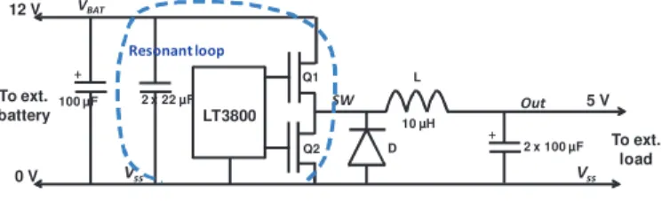
The studied synchronous buck converter is mounted on a 55x58 mm four-layer board designed to characterize conducted emissions. This type of circuit is one of the major contributors of conducted and radiated emission in electronic systems. A simplified schematic of the converter is presented in Fig. 1. It is based on the LT3800 controller from Linear Technology, configured in step-down operation to convert the 12 V voltage provided by a battery into a 5 V regulated voltage for a maximum current of 10 A. This circuit drives the gates of two power NMOSFET STB140NF75 (Q1 and Q2) mounted in D2PAK package. A Schottky diode MBR1660 (D) is mounted in parallel to the NMOSFET Q2. The switching frequency is set to 200 kHz. An external dummy load is connected to the regulated output node (Out) during the CE characterizations. 12 V ! ! To ext. load LT3800 L D !"# 5 V To ext. battery $%&' $(( 0 V )* $(( Q1 Q2 10 µH 2 x 100 µF 100 µF 2 x 22 µF !"#$%&%'()$$*
Fig. 1. Electrical diagram of the studied DC-DC converter
The DC-DC converter is powered by a battery through a long cable harness, which can produce significant radiated emission RE due to high frequency current that flows along it. The characterization of the CE produced by the DC-DC converter follows the recommendations given by CISPR16 standard. The measurements are done in a semi-anechoic chamber. The DC-DC converter is connected to the power supply source through a 1.2 m cable, placed at 5 cm over a large conductive ground reference plane, and a (50 !H+5 ")//50 " LISN compliant to CISPR16-1-2. A current monitor clamp is also added to measure the CM current that circulates along the cable harness, which is mainly responsible of
parasitic RE. These different measurements are done with a receiver configured in peak detection mode.
IV. MODELING OF THE DC-DC CONVERTER BOARD
In the following parts, the definition of the electronic board terminals and the modeling process of its different subparts are described. The proposed models are SPICE compatible.
A. Definition of the board model terminals
The DC-DC converter board has four physical terminals: two power supply terminals connected to VBAT and VSS nodes,
and two others for the connection of the external load connected to Out and VSS nodes. During the CE tests, the
board is mounted above a reference ground plane. The bottom layer of the board, which is a full ground plane, can be directly connected to the reference plane through a ground bonding, or can be left floating. A non-physical port is added to the board model to add an equivalent circuit of the coupling between the board ground plane and the reference plane of the CE test bench.
B. Modeling of the components
Various components have to be modeled to simulate the conducted emission produced by the DC-DC converter. The high frequency noise is related to switching of NMOSFET and Schottky diode on the external load. The input and output filtering capacitors and the inductor L affect the high frequency noise propagation. Unfortunately, no models of these devices were available, so equivalent models have been built from Z(f), I(V) and C(V) measurements.
1) Passive device modeling
Two-port S parameter measurements are performed with a vector network analyzer (VNA) to characterize the impedance profile in frequency domain of these devices. Electrical equivalent models are then extracted. For example, Fig. 2 presents the structures of the model of one tantalum capacitor placed at the converter output. The capacitor model contains several parallel R-C and R-L cells to reproduce the complex frequency behavior of its ESR, that dominates between 100 kHz and 10 MHz. Good agreements between measured and simulated impedance profiles are obtained up to 1 GHz.
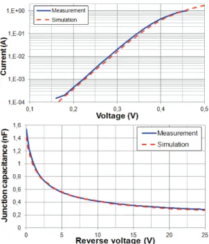
The Schottky diode modeling requires additional measurements. First, I(V) and C(V) characterizations are done with the curve tracer Agilent B1505A to extract the static characteristic of the device and the voltage dependence of its junction capacitance. The diode is modeled as a SPICE diode. An optimization algorithm based on the Levenberg-Marquardt method is used to extract the SPICE model parameters from the I(V) and C(V) curves. A good fit between measured and simulated curves is observed, as shown in Fig. 3. Finally, the parasitic inductance of the Schottky diode, which is mainly related to its package, is extracted from a two-port S parameter measurement. It is estimated to 8 nH.
Fig. 2. (Top): Model of a 100 µF tantalum capacitor (Vishay TR3C107K); (Bottom): Comparison between measurement and simulation of its impedance
Fig. 3. Comparison between measurement and simulation of the I(V) and
C(V) curves of the Schottky diode
2) Power MOSFET modeling
MOSFET modeling from measurement curves is a challenging task because of their non-linear behavior. Numerous MOS device models exist, with more or less complex formulations. The simplest one is Level 1 model and contains few parameters, but it is too trivial to reproduce accurately the complex drain current dependence to gate and drain voltages. Moreover, it does not provide an accurate modeling of gate capacitances. Complex models such as those from BSIM model family are able to reproduce the complex behavior of MOS devices with a large set of empirical parameters. The main drawback is related to the parameter
extraction process from measurements that requires complicated algorithms or expensive equipments.
For CE modeling purpose, only the I(V) characteristic, gate and junction capacitances and parasitic inductances due to the package are required. They can be obtained by measurement. In this work, we propose to model MOSFET static operation with the Sakurai-Newton model [4], which was originally developed to describe the static behavior of short channel MOS devices both in linear and saturation regions. The main advantage of this analytical model is its ability to reproduce the static behavior of MOS device with only six parameters and with a better accuracy than Level 1 model. I(V) measurements are performed on the MOSFET with a high power pulse curve tracer Tektronix 371. The drain current is measured for various drain and gate voltages. An optimization algorithm based on a Nelder-Mead method is then used to tune the parameters of the Sakurai Newton model from the measurement curves. The comparison between measured and simulated I(V) curves of the power MOSFET is presented in Fig. 4. Although the agreement is not perfect, the model reproduces correctly the evolution of the drain current according to the drain and gate voltages and the on-state channel resistance RDS(on).
Fig. 4. Comparison between measurement and simulation of the I(V) curves
of the power NMOSFET
Fig. 5. Comparison between measurement and simulation of the C(V) curves
of the power NMOSFET junction capacitors
Although the Sakurai-Newton model does not include MOSFET parasitic capacitances, they can be added to the model. The non-linear capacitances are extracted from C(V) measurements done between the different terminals of the MOSFET. The comparisons between measurements and simulations of Cds, Cgs and Cgd capacitances are presented in Fig. 5. Two-port S parameter measurements are also performed between the terminals power MOSFET to extract the parasitic inductances associated to the package. Moreover,
the junction capacitance of the MOSFET are affected by parasitic resistive losses. As highlighted in [5], they contribute to damp the ringing observed during the rising transition of the SW node. That's why they should be carefully determined.
3) Gate driver modeling
We assume that the conducted emission produced by the gate driver can be neglected compared to the contribution to the power MOSFET switching on the terminal load. The gate drivers are modeled as voltage source delivering pulse signals whose duty cycle depends on the regulated voltage. The voltage time-domain profiles during transitions are extracted from oscilloscope measurements done on the SW node. Although the gate command frequency is not perfectly stable, the modeled command does not include this intrinsic jitter.
C. Modeling of the test board
The PCB model is extracted by numerical simulation with the tool CST PCB Studio. In order to create a SPICE-compatible model, a possible approach consists in extracting a black-box model. In spite of the recent improvements of black-box modeling tools to solve passivity and stability issues, some convergence problems may arise, especially during transient simulation of non-linear devices. In this study, as the PCB is quite small and the frequency range of the noise produced by the converter is limited to 150 MHz (see measurement results in part VI), the effect of PCB interconnect can be accurately modeled by lumped RLC devices extracted from the simulation results. The most important effect to include in the model is the parasitic inductance between the Schottky diode, the MOSFETs and the input decoupling capacitors. As explained in numerous publications such as [6], these devices form a resonant loop as shown in Fig. 1. This resonant circuit is excited at each rising transition of the SW node, leading to a high frequency resonance clearly visible in the emission spectrum. The parasitic capacitance associated to VBAT, SW and Out nodes
are also included in the model.
V. MODELING OF THE CONDUCTED EMISSION TEST BENCH
Models of cable harness, LISN and external dummy loads are necessary to simulate the CE produced by the DC-DC converter. Their models are extracted from S parameters measurements made with a 2-port VNA. However, their models have to include the CM impedance that exists between these devices and the reference plane of the CE test-bench. The accurate modeling of these CM impedances is required to simulate correctly the propagation of common-mode along the cable harness and the DM to CM conversion.
The measurements are performed with these devices mounted over the reference ground plane. Both ports of the VNA are referenced to the reference plane. The S-parameter measurement results provided by the VNA are given in single-ended format, which is not particularly adapted to extract DM and CM impedances. A more appropriate representation is the mixed-mode S-parameter matrix [SMM], which can be
computed from the single-ended S-parameter matrix [S] according to (1), where [T] is the transformation matrix [7].
SDD is related to the DM impedance, SCC to the CM impedance
and SCD or SCD to the DM to CM conversion.
[
]
[ ][ ][ ]
−1 = ! " # $ % & = T S T S S S S S CC CD DC DD MM ,[ ]
! " # $ % & − = 1 1 1 1 2 1 T (1)Fig. 6. (Top): Equivalent electrical model of the LISN; (Bottom):
Comparison between measured and simulated mixed-mode impedances of the LISN
Equivalent electrical models are extracted from these measurements. The measurements of CE show that the CE is negligible above 150 MHz, as it will be shown in the part V. Thus, the model validity range is extended up to 200 MHz. Fig 6 presents the equivalent electrical model of the LISN. It reproduces quite well the DM and CM impedances, and also the DM to CM conversion.
The same set-up is used to extract the CM impedance between the equipment board and the reference plane. When no connection exists between the ground plane of the board and the reference plane, the board common-mode impedance ZCM_board is only capacitive up to 200 MHz. It depends on
the board dimensions and the distance between the board and the reference plane. The CM capacitance between a rectangular board and a large reference plane can be estimated according to the following closed-form formula[8]:
S S h S C C CCM P i r + + = + =
π
ε
ε
ε
0 15.7 0 1 . 1 (2)where Cp includes the plane capacitance between the board and the reference plane and the fringing capacitance, Ci the intrinsic capacitance of the board, S is the surface of the
board and h the height between the board and the reference plane. Fig. 7 compares the evolution of the CM capacitance according to the board height h computed either with an EM numerical simulation tool or equation (2). Measurement results extracted for three board height values are also added. An excellent agreement is obtained between both models. Their relevance is confirmed by measurement results.
Fig. 7. Comparison between measurement and simulation of the CM
capacitance between the board converter and the reference plane
For a separation distance of 5 cm, the CM capacitance of the equipment board is about 3 pF. At larger frequencies, the resonances of the cavity formed by the PCB ground plane and the reference plane of the CE test bench should be taken into account.
Another important CM impedance is formed by the parasitic capacitance between the SW node of the DC-DC converter and the reference plane. As the SW node is placed at the output of the NMOSFET, it is submitted to large dV/dt which lead to non negligible CM current. Electromagnetic simulations were done to extract the value of this parasitic capacitance with FEKO software. Its value depends on the board height to the reference plane, the SW node surface, the thickness of the board and the permittivity of the dielectric material. For a height of 50 mm, the parasitic capacitance is about 0.15 pF.
VI. SIMULATION OF THE CONDUCTED EMISSION PRODUCED BY THE DC-DC CONVERTER BOARD
In the following part, an external dummy load which consists of a 4.7 " resistor in series with an inductance of 2.5 µH. Moreover, the ground plane of the PCB is not directly bonded to the reference plane. Fig. 8 presents a block diagram of the CE simulation model, showing its different parts. Measurements are done in frequency domain with an EMI receiver. In order to take into account the effect of the IF filter of the receiver, transient simulations followed by a post-processing based on the method described in [9] are done. SPICE simulations are done with LTSPICE while post-processing is done with the freeware IC-EMC.
Fig. 9 compares the measured and the simulated transient profile of the voltage on SW node, during rising and falling transitions. The model reproduces correctly the damped oscillation at 34 MHz which appears after the rising transition. This oscillation is related to the resonant loop forming by the
Schottky diode, the MOSFETs and the input decoupling capacitors. DC-DC converter board model Cable harness model LISN model "#$%
Reference ground plane
D u m m y lo a d m o d e l $%&' $ ))+,-!"# $))+./01 $))+234 56789:30(; <=> : 3 0 (; <?> : 3 0 (; $% & ' @< ) A 9 : 3 0 (; $) ) @ <) A 9 : 3 0 (; B?>$(( )* B?>)*
Fig. 8. Conducted emission model of the synchronous DC-DC converter
Fig. 9. Comparison between measurement and simulation of the time domain voltage profile of the SW node
The measured and simulated waveforms observed at the output of the DC-DC converter at rising and falling transitions are superimposed in Fig. 10. The model reproduces correctly the measured output voltage ripple and the HF noise measured at each rising transition of the SW node. Both results prove that the model is accurate enough to reproduce the voltage waveform on the board equipment, and the conducted emission at the output of the converter.
Fig. 10. Comparison between measurement and simulation of the time domain
voltage profile of the Out node
Fig. 11 compares the measured and simulated CE at both LISN measurement terminals. Although emission standards usually limit the measurement range to 30 MHz, we extend the measurement range up to 150 MHz for simulation validation purpose. The model reproduces the asymmetry observed between 20 and 30 MHz due to DM to CM conversion. The
resonance at 34 MHz is also clearly visible. Discrepancies between measurement and simulation in low frequency can be explained by the jitter on the gate driver command, which is not modeled. Discrepancies above 30 MHz can be explained by the weakness of the LISN model.
Fig. 11. Comparison between measurement and simulation of the conducted
emission spectrum measured at LISN terminals
Fig. 12 compares the measurement and simulation of the CM currents flowing through the power cable harness. The CM current is affected by the parasitic capacitance between SW node and the reference plane. Simulation shows also the resonance at 34 MHz. Discrepancies can be explained by the weakness of cable model, especially around resonances.
Fig. 12. Comparison between measurement and simulation of the
common-mode current flowing through the power cable harness
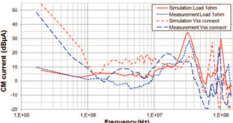
These different comparisons between measurement and simulation results prove the validity of the DC-DC converter board in a given configuration in the CE test bench and for a given terminal load. But the model is also able to simulate correctly the conducted emission when the configuration of the DC-DC converter changes. For example, CE has been measured and simulated in two other configurations: first the dummy load has been changed (4.7 to 1 "); secondly the board ground plane (Vss) has been connected to the reference plane with a bonding wire. In both case, S parameter measurements have been performed to extract equivalent models of the dummy load and the bonding wire. In Fig. 13, measured and simulated CM currents are compared for these two new configurations. In spite some differences, our model simulates correctly the evolution of the CM current, especially its increase due to the decrease of the load in the first case, and the introduction of a path for CM current in the second case. It validates our modeling approach, which simulate CE for various types of configuration (load and test bench) .
Fig. 13. Comparison between measurement and simulation of the CM current for two different configurations: (1): 1 " load; (2): Vss connected to ref. plane
VII. CONCLUSION
The paper has presented a methodology for the development of an electronic board model based on a bottom-up approach. It has been applied on the modeling of the conducted emission of a synchronous buck DC-DC converter. The model is an assembly of component and PCB interconnect models, which can be either provided by component manufacturers or extracted by measurements or simulations. An analysis of the interaction between the board and the nearby environment is required to identify additional ports to connect equivalent model of this interaction. It is essential to take into account common-mode paths.
2343C3-D3(9
[1] A. Durier, C. Marot, O. Crepel, " Using the EM simulation tools to predict the Conducted Emissions level of a DC/DC boost converter : introducing EBEM-CE model", EMC Compo 2013, Nara, Japan.
[2] A. Hamouda, Z. Riah, F. Ndagijimana, S. Serpaud, "Development of
Electronic Board Conducted Emissions Model EBEM-CE using the Bottom-Up Approach", 2014 Int. Symposium on EMC (EMC Europe 2014), Gothenburg, Sweden, Sept. 2014.
[3] IEC62433-2 - EMC IC modelling – Part 2: Models of integrated circuits for EMI behavioural simulation – Conducted emissions modelling (ICEM-CE) - Edition 2.0, January 2017, IEC.
[4] T. Sakurai, R. Newton, “A simple MOSFET model for circuit analysis”,
IEEE Trans. on Electron Devices, vol. 38, pp. 887-894, April 1991. [5] K. Kam, D. Pommerenke, A. Bhargava, B. Steinfeld, C. Lam, F.
Centola, "Quantification of Self-Damping of Power MOSFET in a Synchronous Buck Converter," IEEE Trans. on EMC, vol. 53, no. 4, pp. 1091-1093, Nov. 2011.
[6] L. Middelstaedt, A. Lindemann, M. Al-Hamid, R. Vick, “Influence of
parasitic elements on radiated emissions of a boost converter,” 2015 IEEE International Symp. on EMC on, Aug 2015, pp. 755–760. [7] D. E. Bockelman, W. R. Eisenstadt, "Combined Differential and
Common-Mode Scattering Parameters: Theory and Simulation", IEEE Trans. on Microwave Theory and Techniques, vol. 43, no 7, July 1995.
[8] F. Lafon, "Développement de techniques et de méthodologies pour la
prise en compte des contraintes CEM dans la conception d'équipements du domaine automobile. Etude de l'immunité, du composant à l'équipement", PhD Thesis, Univ. de Bretagne, 2011.
[9] C. Li, L. Zhang, T. Dong, T. Wong, H. Chen, " An EMI Receiver Model
with Consideration of the Intermediate Frequency Filter", 7th Asia-Pacific Int. Symp. on EMC, May 2016.