an author's
http://oatao.univ-toulouse.fr/22804
https://doi.org/10.1016/j.microrel.2018.02.009
Libot, Jean-Baptiste and Alexis, Joël and Dalverny, Olivier and Arnaud, Lionel and Milesi, Philippe and Dulondel,
Frédéric Microstructural evolutions of Sn-3.0Ag-0.5Cu solder joints during thermal cycling. (2018) Microelectronics
Reliability, 83. 64-76. ISSN 0026-2714
Microstructural evolutions of Sn-3.0Ag-0.5Cu solder joints during thermal
cycling
J.B. Libot
a,b,⁎, J. Alexis
a, O. Dalverny
a, L. Arnaud
a, P. Milesi
b, F. Dulondel
baUniversity of Toulouse, INP/ENIT, LGP, 47, Avenue d'Azereix, F-65013 Tarbes, France
bSAFRAN Electronics & Defense, 21, Avenue du Gros Chêne, F-95610 Eragny-sur-Oise, France
Keywords: Lead-free Microstructure Recrystallization
Electron BackScatter Diffraction Temperature cycling Damage
A B S T R A C T
Temperature-induced solder joint fatigue is a main reliability concern for aerospace and military industries whose electronic equipment used in thefield is required to remain functional under harsh loadings. Due to the RoHS directive which eventually will prevent lead from being utilized in electronic systems, there is a need for a better understanding of lead-free thermomechanical behavior when subjected to temperature variations. As solder joints mechanical properties are dependent of their microstructural characteristics, developing accurate solder joint fatigue models means to correctly capture the microstructural changes that undergo the solder alloy during thermal cycling. This study reports the Sn3.0Ag0.5Cu (SAC305) solder joints microstructural evolution during damaging temperature cycles. Electron BackScatter Diffraction (EBSD) analysis was conducted to assess the SAC305 microstructure corresponding to a specific damage level. Investigated microstructural features in-cluded theβ-Sn grain size and crystallographic orientation, as well as the grain boundary misorientation and Ag3Sn intermetallic compound (IMC) size. As-reflowed and damaged components were also mechanically
characterized using nanoindentation technique. The microstructural analysis of SAC305 solder joints prior to thermal cycling showed a highly textured microstructure characteristic of hexa-cyclic twinning with twoβ-Sn morphologies consisting of preferentially orientated macrograins known as Kara's beach ball, along with smaller interlaced grains. The main observation is that recrystallization systematically occurred in SAC305 solder joints during thermal cycling, creating a high population of misoriented grain boundaries leading to intergranular crack initiation and propagation in the high strain regions. The recrystallization process is accompanied with a progressive loss of crystallographic texture and twinning structure. Ag3Sn IMCs coalescence is another strong
indicator of SAC305 solder damage since the bigger and more spaced the IMCs are the less dislocation pinning can prevent recrystallization from occurring.
1. Introduction
Electronic equipment for aerospace and military applications can encounter a wide range of environmental stresses mainly due to ther-momechanical loadings (temperature variations) [1]. With the RoHS directive preventing the use of lead (Pb), lead-free solder joint fatigue in severe temperature environments has been widely studied amongst the electronic industry and academics [2]. While most studies focus on a macroscopic scale approach when assessing thermomechanical be-havior of solder joints, few investigations have been conducted on the effect of thermal cycling on the microstructural evolution of SAC305 solder alloy and the resulting mechanical properties. The micro-structure of SAC305 solder interconnects after reflow consists in a network ofβ-Sn dendrites surrounded by a β-Sn matrix with secondary nanoscale particles of Ag3Sn (eutectic region). Another IMC phase can
appear and depends on the surface finish. For SAC305 solders as-sembled on pure copper, Cu6Sn5will be formed while (Cu,Ni)6Sn5IMCs
develop on ENIGfinished pads [3]. Large primary IMCs can also be formed before the Sn phase during solidification (plate-like shape for Ag3Sn and rod-like for Cu6Sn5). The β-Sn dendrites orientation is
strongly correlated with the crystallographic orientations. As-solidified SAC solder joints generally consist of highly anisotropic β-Sn grains whose size is the same order of magnitude as the joint itself [4,5]. Arfaei et al. studied the influence of solder alloy, volume and pad fin-ishes on the Sn-Ag-Cu solders microstructure and their related ther-momechanical properties. Their investigation showed that two prin-cipal β-Sn grain morphologies were observed after reflow. These morphologies consist of large macrograins and smaller interlaced grains. They also performed Knoop hardness tests and found out that interlaced grains depicted a higher hardness than the macrograins
⁎Corresponding author at: 21, Avenue du Gros Chêne, 95610 Éragny-sur-Oise, France.
E-mail address: [email protected](J.B. Libot).
morphology [6]. Lehman et al. suggested that the macrograins
mor-phology forms from a single point nucleation and is the result of the rapid solidification causing recalescence and therefore inhibiting fur-ther β-Sn grain nucleation. Their work showed that the macrograin and interlaced morphologies respectively result from {101} and {301} cyclic twins [7].This initial microstructure evolves as
thermo-mechanical damage accumulates in solder joints. Recrystallization is a well-known microstructural change occurring in SAC305 solder inter-connects during thermal cycling [8]. As it seems to be the main
da-maging process involved during thermomechanical fatigue of SAC solder joints, every step leading to the creation of recrystallized grains, and eventually solder crack, need to be thoroughly understood. Re-search works have been conducted on the effects of the microstructure of as-soldered solder joints on their thermomechanical fatigue behavior. Bieler et al. studied the influence of β-Sn grains orientation on SAC solder joints thermomechanical response. They reported that a worst-case orientation, where the [001] axis of the β-Sn unit cell is parallel to the substrate, generates a maximum CTE-mismatch, therefore leading to earlier failures. Their findings showed that these randomly dis-tributed orientations seem to be responsible for the usual scattering observed with SAC solder joints [9]. The same author further
in-vestigated the effect of crystal orientations and temperature cycling on the mechanical response of SAC solder interconnects. In-situ synchro-tron X-ray measurements conducted on low-stress Plastic Ball Grid Array (PBGA) components showed that recrystallization process and IMCs coarsening occurring during thermal fatigue tests are unique to each solder joint, making lifetime estimation complex [10]. This work
suggests that there is a correlation between the evolution of the initial microstructure (i.e. β-Sn grains orientations and IMCs distribution) after reflow and recrystallization. Several authors have therefore fo-cused their research on the evolution of these microstructural features during thermal cycling. Coyle et al. conducted thermal cycles on PBGA and resistor components to assess the influence of the as-soldered mi-crostructure on the thermomechanical fatigue durability. By controlling the cooling rate, the number of solder reflows, and isothermal aging, they could indeed form different Ag3Sn IMC particles sizes and spacing.
According to this study, conducting temperature cycles with longer dwell times allow to get rid off the initial microstructure dependency [11]. Terashima et al. performed thermal cycles along with Grain
Boundary Character Distribution (GBSD) imaging and found a corre-lation between the higher number of SAC305 Common Site Lattice (CSL) boundaries and its better thermal fatigue lifetime compared to SAC105 solder joints [12]. Yin et al. conducted thermomechanical
fa-tigue tests on SAC305 solder balls and proposed a damage accumula-tion model based on the evoluaccumula-tion of microstructural features. This study showed that recrystallization occurs between 25% and 50% of the characteristic life, the remaining time being controlled by crack pro-pagation in the recrystallized area [13]. The evolving microstructure
(Ag3Sn coarsening and formation of recrystallized β-Sn grains) during thermal cycling infers an evolution of solder interconnections me-chanical properties. A work conducted by Kanda et al. established a link between the microstructure evolution and the resulting mechanical properties since it focused on the determination of the SAC305 cyclic strain-hardening exponent as a function of the Ag3Sn particles size and
temperature. Their results showed that the exponent was proportional to the reciprocal square root of the average radius of the IMCs, and the effect of temperature on the exponent could be described by the Ar-rhenius function [14]. Sahaym et al. studied the microstructural
coar-sening of Ag3Sn IMCs in SAC305 and SAC105 solder joints during
thermal cycling tests. The authors stated that strain-assisted dissolution and reprecipitation of Ag3Sn particles is accompanied with β-Sn
re-crystallization when an inelastic strain threshold is reached [15]. Sakai
et al. stated that strain hardened metals heated above TH = 0.5 can be
subjected to recrystallization [16]. SAC305 alloy begins to become
li-quid at its solidus temperature equal to 217 °C, meaning that at 20 °C and 125 °C, its homologous temperature is respectively close to
TH ≈ 0.6 and TH ≈ 0.8. In this homologous temperatures range, the
time-dependent material response, that is to say viscoplastic behavior of SAC305 solder alloy, is significant and it is therefore likely to observe recrystallization after thermal cycling between −55 °C and 125 °C. The literature survey shows the complexity of the phenomena leading to failure of lead-free electronic assemblies subjected to thermal cycling loading.
This paper aims to provide a better understanding of the SAC305 microstructure evolution during thermomechanical fatigue tests by assessing every step leading to the fatigue crack and correlating the microstructural changes with a thermomechanical damage level. This correlation is performed through the use of a large spectrum of tech-niques allowing the investigation of the material and mechanical characteristics of SAC305 interconnections. Solder damage is expressed with the creation of recrystallized β-Sn grains through recovery and recrystallization processes. These microstructural modifications come along strain-enhanced Ag3Sn coarsening which appear to be directly
linked to the recrystallization kinetics. Eight industry-representative assemblies consisting in several surface-mount technology components (SMT) including two daisy-chained 900 I/O Wafer Level Packages (WLP900) and two chip resistor (R2512) assembled on a flame re-tardant (FR-4) multi-layered (8 copper ground planes) printed circuit board (PCB) were designed. Thermal cycling tests were conducted be-tween −55 °C and 125 °C, with a 10 °C·min−1 ramp rate and 15 min
dwells, until failure of the sixteen WLP900 and R2512 packages to determine the corresponding number of cycles to failure for a 50% failure rate (N50%) using Weibull distribution. Cross-sections were
performed on additional test coupons whose electrical continuity was not monitored but were taken out of the thermal chamber at different times throughout thermal cycling duration. An in-depth EBSD analysis was then performed to assess the evolution of selected microstructural features. First, an investigation of the as-soldered specimen was con-ducted to identify common characteristics and thus to determine the “finger-print” of non-damaged solder joints. Damaged solder inter-connects were then considered to study the evolution of these main initial microstructural features and their consequences on the occur-rence of recrystallization. A comparison based on nano-indentation hardness measurements was made between an as-reflowed solder joint and a damaged one. Every failed components exhibited solder inter-granular cracks in the high strain regions where recrystallization took place along with Ag3Sn coarsening.
2. Thermomechanical fatigue tests and approach 2.1. Test vehicles and setup
Eight test vehicles consisting of several usual SMT components sembled with SAC305 solder alloy are considered to reflect real as-semblies used in the field. Amongst the mounted packages, two specific components are considered for this paper: a Ball Grid Array-like WLP900 distributed by Topline® and a chip R2512 component manu-factured by KOA® Speer Electronics. The conformal coating opening diameter for the WLP900 component is 0.4 mm and the pitch between each solder ball is 0.25 mm. Concerning the R2512 resistor, the pad length and width are respectively equal to 3.2 and 0.4 mm. According to their solder joints geometry, their size and their material properties, temperature-induced stress in each package solder joints is very dif-ferent and they therefore cover a large spectrum of number of cycles to failure. It is worth noting that the WLP is a technology where the package is the same size as the die. Two of each component are as-sembled per board for a total of sixteen, allowing the statistical analysis of SAC305 solder joints durability. Eight detachable test coupons in-cluding each of the selected packages are also designed for the micro-structure investigation. The substrate is a 220 × 220 mm, 1.6 mm thick multi-layered (ground copper planes) FR-4 printed circuit board. The board has Electroless Nickel Immersion Gold (ENIG) surface finish on
non-solder mask defined (NSMD) pads. It is important to note that the test vehicle considered in this study is representative of real SAC305 assemblies manufactured in the industry.Fig. 1describes the test as-semblies with its corresponding detachable test coupons along with the reflow profile.
Solder joints geometry is an important factor to take into account as it has an influence on the stress/strain distribution within the inter-connection. Solder mechanical response is indeed not homogeneous within the interconnection and the microstructure is also likely to change heterogeneously during the thermomechanical loading. There is
therefore a gradient of properties and microstructural features ac-cording to the localization within the solder joint. Choosing the WLP900 and R2512 components for the study of the SAC305 micro-structure evolution is driven by the fact that they yield different solder joint geometries often met for many different packages.
The test vehicles and coupons are subjected to a military tempera-ture cycles profile following the JEDEC Standard JESD22-A104D test specification [17]:
•
Temperature excursion:−55 °C to 125 °C•
Ramp rate: 10 °C·min−1•
Dwell time: 15 minThe Coefficient of Thermal Expansion (CTE) mismatch between the constitutive materials of the PCB and the components drives the gen-eration of temperature-induced shear strains within solder joints eventually leading to crack initiation and propagation causing compo-nent failure. Test boards are placed in a thermal chamber and con-nected to a data logger system allowing the continuous measurement of the electrical continuity. Except for the test coupons whose components resistance is checked out with a multimeter after removal from the thermal chamber, the daisy-chain resistance of each component is monitored throughout the thermal cycling test at the middle of each dwell time at low and high temperature in order to detect the number of cycles to failure (Fig. 2). The failure criterion is based on the 20% in-crease in resistance forfive consecutive scans according to the IPC-9701A standard [18]. Thermal cycling test is conducted until a max-imum number of temperature cycles is reached. According to previous simulations and return on experience, this maximum number of tem-perature cycles is assumed to cause the failure of most of the WLP900 and R2512 components. This threshold value is set to 3200 cycles. A temperature probe (PT100 resistance) is also placed at the center of each board to allow the determination of the actual thermal cycle the assemblies are subjected to. Given the multi-layered PCB structure with copper ground planes, the overall thermal conductivity of the board is high enough to ensure temperature profiles relatively close to the input thermal chamber temperature.
2.2. Test procedure and matrix
The overall approach to assess the effect of thermal cycling on SAC305 microstructure first consists in conducting the temperature cycles test until failure of each considered component in order to get their associated number of cycles to failure (N50%). Cross-sections are
(a) (b) 0 50 100 150 200 250 0 50 100 150 200 250 300 Tem pera ture ( °C) Time (s)
Fig. 1. (a) Test vehicle with the associated test coupon. (b) Corresponding reflow profile.
-80 -30 20 70 120 0 10 20 30 40 50 60 Tem pera ture ( °C) Time (min)
•
β-Sn grain size,•
β-Sn grain crystallographic orientation,•
Grain boundary misorientation,•
Ag3Sn IMC particles size.The EBSD analysis was conducted using a Nordlys II S camera and micrograph cartographies were performed with a 0.10μm pitch. The EBSD images were then post-processed using AZtec software from Oxford Instruments. Nanoindentation tests were also performed in order to mechanically characterize the SAC305 microstructure after reflow and for a damaged solder joint. The nanoindentation tests were performed using a MTS Nano Indenter®XP. A Berkovich pyramidal nano-indenter was used at a penetration rate of 0.05 s−1during the loading phase. The load was then kept constant during 10 s when the indenter reached a depth of 500 nm. The unloading wasfinally set at a rate of 0.05 s−1. The corresponding hardness was measured for at least
20 indents in order to have statistical results.Fig. 3describes the ap-proach used in this work to study the microstructural evolution of SAC305 solder joints during thermal cycling.
Each test coupon is gradually collected from the thermal chamber throughout the thermal cycling test and the number of corresponding cycles (nout) are arbitrary chosen (though regularly spaced). The
thermal cycling test is conducted until 3200 cycles.Table 1summarizes the successive collection of each test coupon during temperature cycles,
Fig. 3. SAC305 microstructural evolution investigation approach. Table 1
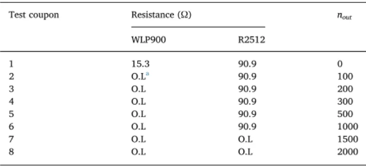
Test coupons resistance and corresponding elapsed time removal (nout).
Test coupon Resistance (Ω) nout
WLP900 R2512 1 15.3 90.9 0 2 O.La 90.9 100 3 O.L 90.9 200 4 O.L 90.9 300 5 O.L 90.9 500 6 O.L 90.9 1000 7 O.L O.L 1500 8 O.L O.L 2000
aO.L = Open Loop (infinite resistance) → a total crack has propagated through the
solder joint.
then performed on the selected components from the test coupons taken out of the thermal chamber at different times during temperature cy-cling (100, 200, 300, 500, 1000, 1500 and 2000 cycles). The metallo-graphic investigation is then conducted using white/polarized light microscopy and Scanning Electron Microscopy (SEM) observations along with EBSD analysis in these specific areas. Four main micro-structural features are considered in this study:
=
D n
N solderi outi
50% (1)
A damage level of 0 corresponds to an as-reflowed test coupon which has not been subjected to any thermomechanical cyclic loading. The microscopic observations followed by EBSD analysis of each cross-section will provide a “snapshot” of the instantaneous evolving mi-crostructure corresponding to a specific damage level in the solder joint.
3. Results and discussion 3.1. Thermal cycles test
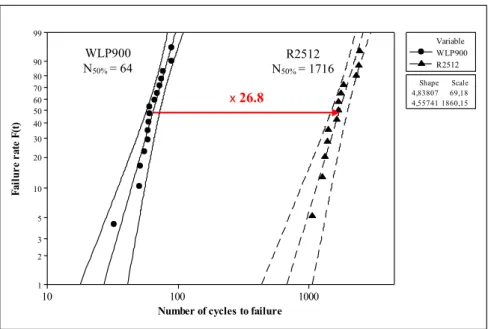
Temperature cycling is conducted until 3200 cycles. The raw elec-trical continuity measurements from the data acquisition system are analyzed to obtain the lifetime of each WLP900 and R2512 component assembled on the test vehicles. This set of lifetimes is then computed to get the corresponding number of cycles to failure for a 50% failure rate. A two-parameter Weibull distribution is thus used to model the number of cycles to failure (Eq.(2)).
= − ⎡ ⎣ ⎢−
( )
⎤⎦⎥ F t( ) 1 e t η β (2) where F(t) is the cumulative failure distribution function or failure rate, η the characteristic life (number of cycles to failure for 63.2% of failed specimens) andβ the shape parameter.Fig. 4presents the Weibull plots corresponding to the WLP900 and R2512 populations. The associated number of cycles to failure for a 50% failure rate can then bedetermined. Under the specific experimental conditions, the R2512 durability is 26.8 times more important than the WLP900 durability.
Some R2512 components did not fail before the end of the thermal cycling test. This was taken into account by using right-truncated data with Minitab software. The test coupons 1 and 2 for WLP900 along with 1, 5, 6, 7, and 8 for R2512 are selected for cross-sectioning and EBSD analysis (bold characters in Table 2). Between 100 and 200 cycles, every WLP900 components have already failed and therefore only the as-soldered and one failed components are considered. The damage level can then be correlated to a damaged zone within the solder joints. 3.2. Failure analysis
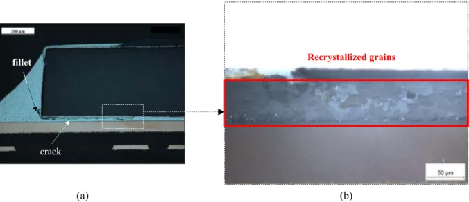
Solder joints damage is electrically expressed with an increase of the daisy-chain resistance. This increase is due to the initiation and pro-pagation of a crack through the solder joint. The regions of high de-formations are correlated with the failure sites. For the WLP900 as-sembly, the crack is located in the solder bulk on the component side (Fig. 5). The crack initiates at the solder neck and propagates along the direction parallel to the solder and component interface. The solder neck is a geometrical singularity due to the WLP900 SMD (Solder Mask Defined) pads which generates a high stress concentration zone from which a crack can nucleate. Concerning the R2512 assembly, the high strain region is localized underneath the component where the crack initiates and propagates to the solderfillet along the component edge
(Fig. 6). When switching from white to polarized light on the optical
microscope, β-Sn grains can be revealed due to their birefringence. While undamaged regions keep their as-reflowed macrograins mor-phology, the high strain zone exhibits recrystallized smaller grains.
This FEM analysis coupled with metallographic observations showed that regardless of the component type and solder shape, cracking occurs in the high strain regions and is accompanied with a recrystallization process where smaller grains are formed. In some rare cases, recrystallization was not observed near the crack path of failed components. It is however important to realize that polarized light is not an accurate observation mean and therefore, the absence of ap-parent smaller grains does not mean that recrystallization did not occur. Polarized light microscopy observations can nevertheless be afirst step to analyze the microstructure of SAC305 solder joints and verify whe-ther obvious recrystallization occurred. It is accordingly a simple and quick way to discriminate cross-sections that might not provide inter-esting information with a costly EBSD analysis.
3.3. As-reflowed SAC305 solder joints microstructure
This section aims to investigate the SAC305 solder joints initial microstructure observed after reflow.Fig. 7presents the initial micro-structure and the associatedβ-Sn grain morphology for an as-solidified SAC305 solder ball. Unlike the macrograins morphology which is sys-tematically observed after reflow, interlaced grains are not always formed and if so, they are often localized at the interface between the solder and the copper pad on component or PCB side. Given the di-rectional dependence ofβ-Sn mechanical properties (Young modulus and CTE), the macrograins morphology therefore confers a strong an-isotropic behavior to the SAC305 solder joints [20]. It is interesting to notice that there is no dendritic structure where the interlaced mor-phology is observed. It is ratherfilled with a homogeneous high density Ag3Sn IMC particles distribution contrary to the rest of the ball whose
dendritic structure yields a heterogeneous and lower Ag3Sn density.
This observation is consistent with the study conducted by Arfaei et al. on SAC305 solder joints [6]. Precipitation-strengthening is therefore enhanced in the interlaced regions. The Ag3Sn repartition, coupled with
the different macrograins crystallographic orientations, creates a me-chanical property gradient within the solder interconnects which makes the SAC305 durability assessment more complex. This initial micro-structure is strongly affected by thermal excursions and temperature-with the measured electrical resistance and the associated removal
number of cycles.
The WLP900 is a 15 × 15 mm component while the R2512 length and width are respectively 6.3 mm and 3.2 mm. Several studies showed that the package size is one of the main factors influencing the assembly thermomechanical durability [19]. For a fixed ΔCTE between the board
and the component, the bigger a component is, the shorter its lifetime will be. It is therefore easily understandable why WLP900 components failed earlier than the R2512 chip resistors. Another preponderant factor to take into account is the CTE of each component. According to the components constitutive materials (Si for the WLP900 and Al2O3 for
the R2512), the WLP900 has a CTE equal to 2.6 ppm·K−1 whereas the
R2512 chip resistor has a CTE of 5.2 × 10⁻⁶ K−1. For the considered
multi-layered PCB, which has a CTE equal to 15 × 10−6 K−1, the CTE
mismatch between the substrate and the assembled component is therefore more important for the WLP900 assembly than the R2512 assembly. The lower solder volume in the case of the WLP900 com-ponent is another factor inducing earlier failures as it provides less strength for the solder joints. It is also worth noting that the time for the crack to propagate is longer for the R2512 chip as the fracture area for this component is approximately 40 times bigger than the fracture area of the WLP900 component (R2512: Acrack ≈ 1.95 mm2, WLP900:
Acrack ≈ 0.05 mm2). Finally, the thermal inertia due to the constitutive
materials of each component also influences the time to failure. WLP900 is made of silicon whose thermal conductivity is about 12 times more important than the thermal conductivity of alumina which is constitutive of the R2512 chip (λSi ≈ 148 W·m−1·K−1,
λAl2O3 ≈ 12 W·m−1·K−1). It is therefore likely that the temperature
excursion, that is to say the damaging level, will be more important for the WLP900. The WLP900 solder balls will therefore be subjected to a quicker damaging process than the R2512 solder joint.
After 3200 cycles, the Weibull distribution is used to compute the measured lifetimes and determine N50% for the WLP900 and R2512
components. The corresponding solder damage level (Dsolder) can be
defined as the ratio between the number of cycles until the test coupon is taken out of the thermal chamber (nout) and the number of cycles to
induced viscoplastic strains which modify the internal structure of each joint.
After identifying the cross-sections depicting these microstructural features, an EBSD analysis has been conducted on an as-reflowed WLP900 solder ball to quantify the selected metallurgical aspects.Fig. 8
(a) shows the initial solder joint microstructure obtained after reflow of a WLP900 component. The macrograins and interlaced morphologies are observed and it is interesting to see that regardless of theβ-grains morphology, the crystallographic orientations are the same. According to the pole figure (Fig. 8(b)), the un-damaged SAC305 solder joint
microstructure is highly textured as the Multiple of Uniform density is ≫1 (MUD = 75.83). There are indeed three privileged orientations as it is depicted with the three colors on the EBSD Inverse Pole Figure (IPF) cartography (yellow, green and red).Fig. 8(c) shows that the solder ball exhibits twin boundaries with near 60° misorientation about the β-Sn [100] or [010] axis (there is a 90° rotation invariance around the [001] axis due to theβ-Sn primitive cell structure). As a consequence, the diagram of misorientation angles presents a high population of grain boundaries around 60° (Fig. 8(d)). This observation is consistent with hexa-cyclic twinning and has been made for every cross-section
1000 100 10 99 90 80 70 60 50 40 30 20 10 5 3 2 1
Number of cycles to failure
Fa il u r e r a te F (t ) 4,83807 69,18 4,55741 1860,15 Shape Scale WLP900 R2512 Variable
x 26.8
WLP900 N50% = 64 R2512 N50% = 1716Fig. 4. Weibull distributions for the WLP900 and R2512 components.
Table 2
Calculated damage in WLP900 and R2512 solder joints for each test coupon (red: total crack/green: no or partial crack).
Test coupon Dsolder
WLP900 R2512 1 0 0 2 1.56 0.06 3 3.13 0.12 4 4.69 0.17 5 7.81 0.29 6 15.63 0.58 7 23.44 0.87 8 31.25 1.17
(a)
(b)
macrograins recrystallized grains crackFig. 5. (a) Observation of the thermomechanical fatigue crack localized in the solder bulk on the component side. (b) Polarized light observation of the recrystallization near the crack path.
(a)
(b)
Recrystallized grains
fillet
crack
Fig. 6. (a) Observation of the thermomechanical fatigue crack localized in the solder bulk underneath the R2512 chip. (b) Polarized light observation of recrystallization near the crack path.
(a)
(b)
(c)
(d)
Primary Ag
3Sn
plates
no dendritic structure
interlaced grains
macrograins
β-Sn matrix
+Ag
3Sn
β-Sn dendrite
(Cu,Ni)
6Sn
5Fig. 7. (a) SAC305 solder ball after reflow. (b) Interlaced and macrograins morphologies observed with polarized light. (c) SEM picture showing the SAC305 dendritic microstructure. (d)
EDX analysis showing Ag3Sn IMCsfilling the inter-dendritic spaces (red: Sn phase/blue: Ag phase). (For interpretation of the references to colour in this figure legend, the reader is
from the undamaged test coupons. To sum up, as-reflowed SAC305 solder joints present a highly crystallographic-textured microstructure consisting in three major twin orientations which cyclically repeat about 60° around the [100] axis. These results have been reported by several authors [7,21].
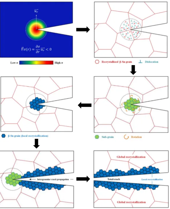
3.4. Evolution of theβ-Sn grains size and crystallographic orientation The evolution ofβ-Sn grains size and the associated textured mi-crostructure observed after reflow has been investigated throughout the temperature cycling test. The thermal cycles generate viscoplastic strains eventually leading to the formation of new smaller grains characteristic of the recrystallization process. Prior to recrystallization, a recovery process occurs. As the viscoplastic strains develop in the solder joints, the created dislocations annihilate and rearrange to form sub-grain boundaries (dislocation walls). These dislocation cells (sub-grains) can then grow due to thermal-activated and strain-enhanced coalescence decreasing their surface energy, and rotate to create higher angle grain boundaries leading to recrystallized β-Sn grains. The
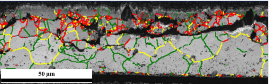
created misoriented grains during recrystallization are highly mis-oriented from each other and high angle grain boundaries are gener-ated, providing a privileged path for crack propagation. The closer to the solder crack, the higher the grain boundary angles (Fig. 9).
Thermomechanical fatigue is always associated with intergranular crack, likely due to a grain boundary sliding (GBS) process occurring under the action of shear stresses during thermal cycling. The following bullets summarize the different steps leading to the thermomechanical fatigue crack:
1) Thermal (especially during high temperature dwells) and strain-enhanced Ag3Sn coarsening,
2) Dislocations motion and rearrangement,
3) β-Sn sub-grains creation with low angle grain boundaries, 4) Rotation ofβ-Sn sub-grains leading to a higher grain disorientation, 5) Creation of recrystallized β-Sn grains with high angle grain
boundaries,
6) Intergranular crack propagation by GBS.
(a)
(b)
(c)
(d)
0 0.05 0.1 0.15 0.2 0.25 0.3 0 20 40 60 80 Rel . f requency Misorientation (deg)High misorientation around 60°
macrograins interlaced grains 200 μm twin boundaries 200 μm
Fig. 8. (a) As-reflowed WLP900 solder ball crystallographic orientations. (b) Associated pole figure. (c) Twin boundaries. (d) Misorientation angles distribution.
Fig. 9. High angle grain boundaries near crack in the high strain region beneath the R2512 component for Dsolder= 0.29 (green: 0°–15°, yellow: 15–45°, red: > 45°). (For interpretation of
As a result, as the thermal cycling is conducted, the major crystal-lographic orientations observed after reflow do no longer exist when solder damage is significant. SAC305 solder joints tend to lose their textured microstructure with the creation of highly misoriented re-crystallized grains. Fig. 10 shows the SAC305 crystallographic or-ientation along with the corresponding polefigures for several R2512 solder joints for three different damage levels. The loss of crystal-lographic orientation is likely due toβ-Sn grains rotations during re-crystallization.
Fig. 11shows theβ-Sn grains size distribution in the R2512 damage
zone corresponding to damage level of 0.29, 0.58, 0.87 and 1.17 (for
Dsolder= 1.17, the EBSD cartography depicting β-Sn grains size is
given). These measurements have been conducted using the EBSD image analysis software embedded in the Oxford Instruments applica-tion (AZtec). Those four EBSD analysis have been performed on failed components (test coupons 7 and 8 as shown inTable 1) and on com-ponents with partial cracks (test coupons 5 and 6). It turns out that regardless of the damage level, the grain size distribution remains the
Fig. 10. Evolution of the SAC305 solder joints crystallographic texture after several thermal cycles: EBSD maps and the associated polefigures for damage levels equal to (a) 0, (b) 0.29,
and (c) 1.17. 0 5 10 15 20 25 30 35 40 1,1 2 3 4 5 6 7 8 9 10 11 12 13 14 15 16 17 18 19 20 >20 Proportion (%)
Equivalent β-Sn grain diameter (μm)
0.29 0.58 0.87 1.17
same. This can mean that the recrystallization kinetics is that quick that β-Sn grains reach a threshold value from which no further evolution occurs. R2512 solder joints from the 8th test coupons nevertheless depict a higher population of large equivalent diameters. The fraction of grain size above 9μm is indeed slightly higher than in the rest of the selected solder joints. This can be the result of the grain growth process occurring at high temperature and thermodynamically driven by the minimization of interfacial energy, where grain boundaries can move and consume neighboring smaller grain, eventually leading to an in-crease inβ-Sn grain size.
It is also interesting to observe that a high proportion of smallβ-Sn grains (≈2 μm) is localized along the crack path (blue grains on the EBSD cartography). An interpretation that could be made regarding this observation is that these smallβ-Sn grains localized around the solder crack can result from a“local” recrystallization process due to the high stress concentration at the crack tip during propagation. Temperature
and strain rate conditions allowing viscoplastic deformations to take place are still met and recrystallization can thus occur.Fig. 12shows the different steps leading to the formation of these localized small β-Sn grains. First, a high stress concentration volume is generated at the crack tip, leading to the creation of dislocations. Then, these disloca-tions can move in this volume and rearrange to formβ-Sn sub-grains (as it occurs during global recrystallization). These dislocation cells have low disorientation angles and further thermal cycling is required to rotate the sub-grains and eventually form smaller recrystallizedβ-Sn grains. The same process repeats itself throughout crack propagation. The schemes depicted inFig. 12present the microstructural evolution in a high strain area of a solder joints where“global” recrystallization already occurred. Future work including FEM analysis would be inter-esting to calculate the stressfield at the crack tip and assess the volume impacted by the local recrystallization.
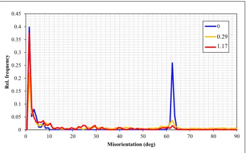
3.5. Evolution of the hexa-cyclic twins
The following section aims to study how the hexa-cyclic twins evolve during thermal cycling. As explained before, the hexa-cyclic twinning is a microstructural characteristic that can be observed on every solder joint cross-section after reflow. One way to analyze the influence on thermal cycling on this parameter is to plot the mis-orientation angles distribution diagrams corresponding to different damage levels.Fig. 13shows the EBSD twin boundaries analysis per-formed on R2512 solder joints, and their associated misorientation angles distribution. It turns out that hexa-cyclic twins tend to disappear as the solder damage increases. There is indeed a smaller population of twin boundaries around 60° and a larger proportion of high angle grain boundaries (angles > 15°), indicating that recrystallized grains are formed. An interesting consequence is that damaged solder joints never exhibits any interlaced grains in the high strain regions.
3.6. Evolution of the Ag3Sn IMC particles size
It is also worth noting that the solder damage is accompanied with a loss of dendritic structure. The damage region rather consists in a tin-matrixfilled with dispersed coarsened Ag3Sn IMC particles. There is
therefore a continuous, though heterogeneous softening within SAC305 solder joints throughout thermal cycles. The thermal-activated coar-sening is also coupled with a strain-enhanced Ag3Sn coarsening process
in the damaged part of the solder joint.Fig. 14shows the increase in Ag3Sn IMCs size in R2512 solder joints during thermal cycles forfive
different damage levels. Ag3Sn particles size was measured with AZtec
software using the equivalent diameter method. While non-damaged SAC305 microstructure exhibits an organized distribution of nano-me-tric Ag3Sn IMC particles in the inter-dendritic spaces, the high strain
regions where cracking occurred, and where high angles grain bound-aries are created, show that large IMCs have coalesced. This observation suggests that strain-enhanced Ag3Sn coalescence is controlled by grain
boundary diffusion. As the coarsening of Ag3Sn particles takes place,
the resistance to dislocation motion decreased. After reflow, nano-me-tric IMCs are finely dispersed and can indeed act as barriers to the viscoplastic strain-induced dislocations motion and inhibit SAC305 solder damage by dislocation pinning process. However, with the in-creasing size of Ag3Sn precipitates coupled with the lower density
(more important spacing between particles), the dislocations are no longer blocked, the large IMCs can constitute good nucleation sites and
recrystallization is thus promoted.
Moreover, Ag3Sn precipitates tend to move towards grain
bound-aries as coalescence takes place. This migration weakens the grain boundaries and is therefore another factor leading to intergranular crack.Fig. 15 shows a SEM picture of coarse Ag3Sn IMCs localized
along the crack path after 1000 thermal cycles.
Thermomechanical damage causes changes in Ag3Sn IMC particles
size and spacing, leading to a localized softening of the SAC305 solder joints. These softened regions do not withstand viscoplastic deforma-tions as they did prior to strain-enhanced coarsening and are therefore likely to be subjected to recrystallization. The evolution of Ag3Sn
pre-cipitates can thus have a significant influence on the resulting SAC305 mechanical properties as it will be investigated in the next section.
3.7. Nanoindentation tests
The correlation between the observed microstructural evolutions and the resulting mechanical properties has been investigated through nanoindentation measurements. WLP900 solder balls have been con-sidered since they provide a large surface to perform the indentation testing. The investigation mainly focused on the mechanical properties of SAC305 solder joints after reflow (0 damage level) and after cracking (damage level > 1). The nanoindentation tests have been conducted using a Berkovich pyramidal indenter and the SAC305 hardness was extracted from load-displacement curves. At least 20 measurements are considered in order to have statistical results regarding the obtained hardness. Fig. 16presents the WLP900 solder balls selected for the mechanical characterization. A non-damaged solder joints depicting interlaced and macrograins morphologies is chosen tofigure the dif-ference between these two microstructural characteristics (Fig. 16(a)). A totally cracked solder ball is then analyzed to assess the hardness of the recrystallized grains compared to the macrograins which are not subjected to large viscoplastic strains (Fig. 16(c)). The bar diagram presenting the hardness in the as-reflowed WLP900 solder ball shows that the interlaced grains resistance to deformation is higher than the resistance of the macrograins from the center of the ball. The Ag3Sn
IMC particles density in interlaced region is indeed more important than in the dendrite-structured macrograins. The created dislocations during indentation are therefore likely to be blocked by these IMCs and a higher hardness is obtained. This observation is also consistent with the study conducted by Arfaei et al., Chen et al. and Xu et al. on SAC305 solder joints [6,22,23]. It is also noteworthy that the SAC305 0 0.05 0.1 0.15 0.2 0.25 0.3 0.35 0.4 0.45 0 10 20 30 40 50 60 70 80 90 Rel. frequency Misorientation (deg) 0 0.27 1.14 0.29 1.17
Fig. 13. Evolution of misorientation angles during thermal cycling test. Twin boundaries tend to disappear as it can be noticed with the yellow (Dsolder= 0.29) and red curves
macrograins hardness does not exhibit large differences according to the crystallographic orientation. Concerning the damaged WLP900 solder joint, the measured hardness in the recrystallized zone is lower than in the rest of the ball. The macrograins still exhibit a similar hardness value regardless of the crystallographic orientation, though it is a lower value than the one measured after reflow since the Ag3Sn
have grown due to thermal-induced coarsening. It is also not surprising tofind a lower hardness level in the damaged area as recrystallization generated stress-free grains whose residual stresses are even more re-laxed after cracking. Measuring the hardness of SAC305 solder joints throughout thermal cycling can constitute a good indicator to assess solder damage. Viscoplastic strains generated during thermal cycling would indeed create strain-hardened sub-grains in the damage regions which would eventually get rid of the accumulated dislocations through the recrystallization process and therefore exhibit a lower hardness. Further measurements are needed to have a better understanding on the evolution of the mechanical properties in the high strain regions.
4. Conclusions
The global approach developed in this study is based on an in-depth microstructural investigation of the evolving SAC305 microstructure along with statistical thermomechanical fatigue results and mechanical char-acterization. According to observations performed on WLP900 and R2512 components, two consecutive processes are believed to occur during thermomechanical damage: recovery and recrystallization. Recovery pro-cess seems to act as a“pre-requisite” for recrystallization. The rearrange-ment of excess dislocations created by viscoplastic strains into low angle tilt boundaries (sub-grain boundaries with low angles misorientation) in-deed causes polygonization to take place and forms grains. These sub-grains are then believed to be subjected to coalescence and rotation during recrystallization, creating high angle grain boundaries which constitute an energetically privileged path for crack initiation and propagation. The resulting component failure is indeed due to thermomechanical fatigue crack caused by grain boundary sliding process.
The main observations of this paper can be summarized as follow:
•
Recrystallization phenomenon is observed in the most deformed region of the solder joint (creation of an equiaxed microstructure before cracking),•
Thermal and strain-enhanced Ag3Sn coalescence occurs and facil-itates recrystallization,•
There is a loss of crystallographic texture during temperature-in-duced damage,•
The interlaced morphology is never observed on damaged solder joints,•
There is an increase of high angle grain boundaries in the high strain regions promoting intergranular crack,•
The intergranular crack propagates by grain boundary sliding,•
Regardless of the damage level, theβ-Sn grain size seems to remain constant after crack propagation,•
Smallerβ-Sn grains (≈ 2 μm) are observed along the crack path,•
Interlaced morphology regions exhibit a higher Berkovich hardness likely due to the high density of Ag3Sn nano-particles,•
Recrystallized grains exhibit a lower hardness compared to the rest of the solder interconnect due to the stress release and the coarse Ag3Sn IMCs in these areas.(a) (b) (c) (d) 0.72 0.95 0.97 1.10 1.03 0.0 0.2 0.4 0.6 0.8 1.0 1.2 1.4 0 0.29 0.58 0.87 1.17 Ag 3 ) m μ( e zi s s el ci t r a p n S Damage level
Fig. 14. Ag3Sn particles identification for a damage level of (a) 0, (b) 0.58, and (c) 1.17. (d) Evolution of Ag3Sn precipitates (colored in red on the EBSD cartography) during thermal
cycling test. (For interpretation of the references to colour in thisfigure legend, the reader is referred to the web version of this article.)
Fig. 15. Coarse Ag3Sn precipitates localized at the crack path (example of a R2512 with a
Acknowledgments
This research work was partially supported by the University of Toulouse and Safran Electronics & Defense. The authors would like to thank M.A. Bahi and J.C. Riou for their insightful comments regarding the EBSD analysis.
References
[1]D. Steinberg, Vibration Analysis for Electronic Equipment, 3rd edition, John Wiley & Sons, Inc., 2000.
[2]W.W. Lee, L.T. Nguyen, G.S. Selvaduray, Solder joint fatigue model: review and applic-ability chip scale packages, Microelectron. Reliab. 40 (2) (2000) 231–244.
[3]A. Choubey, Microstructural Changes Under Isothermal Aging and Their Influence on Thermal Fatigue Reliability for Tin-lead and Lead-free Solder Joints, Including Microstructural Changes Under Isothermal Aging in Mixed Solder Joints (PhD Thesis Dissertation), University of Maryland, 2007.
[4]S. Mukherjee, B. Zhou, A. Dasgupta, T.R. Bieler, Multiscale Modeling of the Anisotropic Transient Creep Response of Heterogeneous SAC Single Crystal, 16th International Conference on Thermal, Mechanical and Multi-Physics Simulation and Experiments in Microelectronics and Microsystems, 2015.
[5]D. Barbini, M. Meilunas, Reliability of Lead-Free LGAs and BGAs: Effects of Solder Joint Size, Cyclic Strain and Microstructure, SMTA International Conference Proceedings, 2011.
[6]B. Arfaei, L. Wentlent, S. Joshi, A. Alazzam, T. Tashtoush, M. Halaweh, S. Chivukula, L. Yin, M. Meilunas, E. Cotts, P. Borgesen, Improving the Thermomechanical Behavior of Lead Free Solder Joints by Controlling the Microstructure, 13th InterSociety Conference on Thermal and Thermomechanical Phenomena in Electronic Systems, 2012, pp. 392–398.
[7]L.P. Lehman, Y. Xing, T.R. Bierler, E.J. Cotts, Cyclic twin nucleation in tin-based solder alloys, Acta Mater. 58 (2010) 3546–3556.
[8]K. Holderlann, G. Cuddalorepatta, A. Dasgupta, Dynamic recrystallization of Sn3.0Ag0.5Cu Pb-free solder alloy, Proceedings of ASME IMECE 6 (2008) 163–169. [9]T.R. Bieler, H. Jiang, L.P. Lehman, T. Kirkpatrick, E.J. Cotts, B. Nandagopal, Influence of
Sn grain size and orientation on the thermomechanical response and reliability of Pb-free solder joints, IEEE Transactions on Components and Packaging Technologies 31 (2) (2008) 370–381.
[10] T.R. Bieler, B. Zhou, L. Blair, A. Zamiri, P. Darbandi, F. Pourboghrat, T.-K. Lee, K.-C. Liu, The role of elastic and plastic anisotropy of Sn in recrystallization and damage evolution during thermal cycling in SAC305 solder joints, J. Electron. Mater. 41 (2) (2012) 283–301.
[11] R. Coyle, J. Osenbach, M.N. Collins, H. McCormick, P. Read, D. Fleming, R. Popowich, J. Punch, M. Reid, S. Kummerl, Phenomenological study of the effect of microstructural evolution on the thermal fatigue resistance of Pb-free solder joints, IEEE Transactions on Components, Packaging and Manufacturing Technologies 1 (10) (2011) 1583–1593. [12] S. Terashima, T. Kohno, A. Mizusawa, K. Arai, O. Okada, T. Wakabaashi, M. Tanaka,
K. Tatsumi, Improvement of thermal fatigue properties of Sn-Ag-Cu lead-free solder in-terconnects on Casio's wafer-level packages on morphology and grain boundary char-acter, J. Electron. Mater. 38 (1) (2009) 33–38.
[13] L. Yin, L. Wentlent, L. Ang, B. Arfei, A. Oasaimeh, P. Borgesen, Recrystallization and precipitate coarsening in Pb-free solder joints during thermomechanical fatigue, J. Electron. Mater. 41 (2) (2012) 241–252.
[14] Y. Kanda, Y. Kariya, T. Tasaka, Effect of strain-enhanced microstructural coarsening on the cyclic strain-hardening exponent of Sn-Ag-Cu joints, Mater. Trans. 53 (12) (2012) 2072–2077.
[15] U. Sahaym, B. Talebanpour, S. Seekins, I. Dutta, P. Kumar, P. Borgesen, Recrystallization and Ag3Sn particle redistribution during thermomechanical treatment of bulk Sn-Ag-Cu
solder alloys, IEEE Transactions on Components, Packaging and Manufacturing Technologies 3 (11) (2013) 1868–1875.
[16] T. Sakai, A. Belakov, R. Kaibshev, H. Miura, J.J. Jonas, Dynamic and post-dynamic re-crystallization under hot, cold and severe plastic deformation conditions, Prog. Mater. Sci. 60 (2014) 130–207.
[17] JEDEC Standard,“Temperature Cycling”, JESD22-A104D, (2005).
[18] IPC-9701A, Performance Test Methods and Qualification Requirements for Surface Mount Solder Attachments, Association Connecting Electronics Industries, 2006.
[19] J.H. Lau, The role of DNP (distance to neutral point) on solder joint reliability of area array assemblies, Soldering & Surface Mount Technology 9 (2) (1997) 58–60. [20] S. Yang, Y. Tian, C. Wang, T. Huang, Modeling thermal fatigue in anisotropic Sn-Ag-Cu/
Cu solder joints, ICEPT-HDP (2009) 288–289.
[21] M. Mueler, S. Wiese, K.-J. Wolter, The twinning phenomenon in SnAgCu solder balls, Electronic Components and Technology Conference (2009) 1027–1036.
[22] H. Chen, J. Han, J. Li, M. Li, Inhomogeneous deformation and microstructure evolution of Sn-Ag-based solder interconnects during thermal cycling and shear testing,
Microelectron. Reliab. 52 (2012) 1112–1120.
[23] X. Xu, G. Chen, M. Cheng, Study on local recrystallization and damage mode of lead-free BGA solder joint, International Conference on Electronic Packaging Technology (2014) 356–359.
(a)
(b)
(c)
(d)
0.342 0.302 0.298 0 0.05 0.1 0.15 0.2 0.25 0.3 0.35 0.4Interlaced morphology Area 1 Area 2
Har dne ss (GP a ) 0.280 0.272 0.234 0 0.05 0.1 0.15 0.2 0.25 0.3 0.35 0.4
Area 1 Area 2 Recrystallized grains
Har d nes s ( GP a) Interlaced morphology Area 2 Area 1 Recrystallized grains Area 2 Area 1
Fig. 16. (a) Cross-section of a WLP900 as-reflowed solder ball exhibiting interlaced and macrograins morphologies. (b) Associated hardness results. (c) Cross-section of a WLP900 damaged solder ball. (d) Hardness in the recrystallized region and in the center of the ball.