Université de Montréal
FPGA-Based Object Detection Using
Classification Circuits
par Min Fu
Département d’informatique et recherche opérationnelle Faculté des arts et des sciences
Mémoire présenté à la Faculté des arts et des sciences en vue de l’obtention du grade de Maître ès sciences
en informatique
Avril 2015
i
Résumé
Dans l'apprentissage machine, la classification est le processus d’assigner une nouvelle observation à une certaine catégorie. Les classifieurs qui mettent en œuvre des algorithmes de classification ont été largement étudié au cours des dernières décennies. Les classifieurs traditionnels sont basés sur des algorithmes tels que le SVM et les réseaux de neurones, et sont généralement exécutés par des logiciels sur CPUs qui fait que le système souffre d’un manque de performance et d’une forte consommation d'énergie. Bien que les GPUs puissent être utilisés pour accélérer le calcul de certains classifieurs, leur grande consommation de puissance empêche la technologie d'être mise en œuvre sur des appareils portables tels que les systèmes embarqués. Pour rendre le système de classification plus léger, les classifieurs devraient être capable de fonctionner sur un système matériel plus compact au lieu d'un groupe de CPUs ou GPUs, et les classifieurs eux-mêmes devraient être optimisés pour ce matériel.
Dans ce mémoire, nous explorons la mise en œuvre d'un classifieur novateur sur une plate-forme matérielle à base de FPGA. Le classifieur, conçu par Alain Tapp (Université de Montréal), est basé sur une grande quantité de tables de recherche qui forment des circuits arborescents qui effectuent les tâches de classification. Le FPGA semble être un élément fait sur mesure pour mettre en œuvre ce classifieur avec ses riches ressources de tables de recherche et l'architecture à parallélisme élevé. Notre travail montre que les FPGAs peuvent implémenter plusieurs classifieurs et faire les classification sur des images haute définition à une vitesse très élevée.
Abstract
In the machine learning area, classification is a process of mapping a new observation to a certain category. Classifiers which implement classification algorithms have been studied widely over the past decades. Traditional classifiers are based on algorithms such as SVM and neural nets, and are usually run by software on CPUs which cause the system to suffer low performance and high power consumption. Although GPUs can be used to accelerate the computation of some classifiers, its high power consumption prevents the technology from being implemented on portable devices such as embedded systems or wearable hardware. To make a lightweight classification system, classifiers should be able to run on a more compact hardware system instead of a group of CPUs/GPUs, and classifiers themselves should be optimized to fit that hardware.
In this thesis, we explore the implementation of a novel classifier on a FPGA-based hardware platform. The classifier, devised by Alain Tapp (Université de Montréal), is based on a large amount of look-up tables that form tree-structured circuits to do classification tasks. The FPGA appears to be a tailor-made component to implement this classifier with its rich resources of look-up tables and the highly parallel architecture. Our work shows that a single FPGA can implement multiple classifiers to do classification on high definition images at a very high speed.
iii
Contents
Résumé ... i Abstract ... ii Contents ... iii List of Tables ... v List of Figures ... viList of Abbreviations ... viii
Acknowledgements ... ix
Chapter 1 – Introduction ... 1
1.1 Introduction of FPGA ... 2
1.2.1 Advantages and disadvantages ... 3
1.2.2 FPGA Design Methodology ... 4
1.2 Organization of the thesis ... 5
Chapter 2 – A novel classifier ... 6
2.1 The framework ... 6
2.2 Learning algorithms ... 7
2.3 Object detection ... 11
Chapter 3 - Hardware architecture ... 12
3.1 FPGA design ... 12
3.2 Ethernet interface ... 14
3.3 External memory ... 17
3.4 Sliding window ... 19
3.5 Classifiers ... 21
Chapter 4 – Timing design ... 22
4.1 Ethernet frame reception and transmission ... 22
4.2 Data buffer between receiver and DDR3 memory ... 23
4.3 External memory user design ... 28
4.3.2 Write data path ... 29
4.3.3 Read data path ... 30
4.1.3.4 FSM for read/write management ... 31
4.4 Image processing ... 32
4.4.1 Data loss problem in the asynchronous RAM ... 32
4.4.2 Subwindow's data ... 33
4.4.3 Classification and results buffering ... 35
Chapter 5 – Evaluation ... 36
5.1 System Simulation ... 36
5.2 Functional verification ... 37
5.3 FPGA evaluation ... 40
Chapter 6 – Conclusion and future works ... 44
v
List of Tables
Table 1: 2-gate example ... 8
Table 2: An example of building the truth table for a Gate ... 9
Table 3: Signals of command path ... 28
Table 4: Signals of write data path ... 29
Table 5: Signals of read data path ... 31
List of Figures
Figure 1: FPGA Architecture [19] ... 2
Figure 2: A Simplified Logic Block [20] ... 3
Figure 3: FPGA Design Flow [24]... 4
Figure 4: Tree-structured Classifier ... 6
Figure 5: Leaves of the tree are connected to input data bits randomly ... 7
Figure 6: Replace a leaf by another input bit to update the classifier ... 10
Figure 7: A sliding window should move from left top of the image to the right bottom 11 Figure 8: High-level architecture and data flow between the PC and FPGA ... 12
Figure 9: FPGA architecture containing all the main blocks ... 13
Figure 10: Block Description of KC705 FPGA Evaluation Board [28] ... 14
Figure 11: OSI reference model [29] ... 15
Figure 12: Standard Ethernet Frame Structure [30] ... 15
Figure 13: Ethernet Interface in FPGA containing MAC and FIFOs ... 16
Figure 14: Input and output signals of Ethernet Interface block ... 17
Figure 15: Memory Interface Core Architecture [31] ... 18
Figure 16: User Design block for data transmission between FPGA and external memory ... 19
Figure 17: The sliding window constructed by Regular shift registers from different rows ... 20
Figure 18: Description of how to get a subwindow by shifting data between shift registers ... 21
Figure 19: Data from the sliding window are fed to independent classifiers in parallel .. 21
Figure 20: AXI4-stream interface implemented in Ethernet Interface ... 23
Figure 21: Frame reception of AXI4-Stream interface at 1Gbps ... 23
Figure 22: Frame transmission of AXI4-Stream interface at 1Gbps ... 23
Figure 23: FSM in the Rx_buffer block ... 24
Figure 24: Write a frame to the RAM ... 25
vii
Figure 26: Metastable state (1) [35] ... 26
Figure 27: Metastable state (2) [35] ... 27
Figure 28: A two-flop synchronizer ... 27
Figure 29: Command path timing [31] ... 29
Figure 30: timing of a single write operation [31] ... 30
Figure 31: Timing of two reading operations [31]... 31
Figure 32: FSM for read/write management ... 32
Figure 33: Avoid data loss problem in asynchronous digital design ... 33
Figure 34: Data flow of Shift registers (1) ... 34
Figure 35: Data flow of Shift registers (2) ... 34
Figure 36: Two classifiers output the results simultaneously ... 35
Figure 37 Testbench for system simulation ... 37
Figure 38: Verification system... 37
Figure 39: Software flowchart ... 38
Figure 40: Image of handwritten digits ... 39
Figure 41: Ethernet frames received by the software ... 39
Figure 42: Results in the image ... 40
Figure 43: FPGA device utilization reported by ISE ... 41
Figure 44: On-chip power consumption ... 41
Figure 45: Routed wires viewed by FPGA Editor ... 41
Figure 46: The sending speed of software ... 43
List of Abbreviations
FPGA: Field Programmable Gate Array SVM: Support Vector Machines
GPU: Graphics Processing Unit CLB: Configurable Logic Block LUT: Look-Up Table
ASIC: Application Specific Integrated Circuit DDR: Double Data Rate
MAC: Media Access Control OSI: Open Systems Interconnection AXI4: Advanced Extensible Interface 4 FSM: Finite State Machine
ix
Acknowledgements
I would like to express my sincere gratitude to my supervisor Marc Feeley, who introduced me to research this topic. Without his help and guidance, this work would not have been completed. I am very grateful to my co-supervisor Alain Tapp for his support on my research and thesis.
I would also like to thank my colleagues in our Lab: Maxime Chevalier-Boisvert, Vincent Archambault-Bouffard, Baptiste Saleil and Benjamin Cerat for their help in my research and my school life.
Finally, I would like to dedicate all my achievements to my family, especially to my wife Si Chen, for their support and encouragement.
Chapter 1 – Introduction
Machine learning is a scientific discipline that explores the construction and study of algorithms that can learn from data [1]. According to learning rules, machine learning has two types of learning: supervised learning and unsupervised learning. An important supervised learning task is classification, where, given a set of examples and their classes, a learning algorithm learns a classifier that assigns a new input example to one of the classes [2]. Unsupervised learning is the task to find hidden structure from unlabeled data [3]. In this work, we use supervised learning to produce the classifier.
Currently, classifiers have been applied to many use cases, such as email classification [4], natural language processing [5] and medical diagnosis [6]. Most classification problems are computationally expensive problems [7]. Researchers keep proposing new ideas to build more accurate and faster classifiers to meet the requirements of the applications. Most of the researchers focus on implementing algorithms on conventional platforms such as CPUs, but they are struggling to achieve the high speed performance and suffering low power efficiency on CPUs. Relatively few researchers are trying to explore alternative hardware platforms which have special advantages for high-speed classification tasks.
The FPGA, with its reconfigurable nature and massive parallelism, has been used to achieve high performance computation in both scientific and industrial fields. In the fields of image processing, computer vision, and digital signal processing, the FPGA is becoming increasingly attractive [8]. In the context of object detection, FPGAs have been utilized to accelerate the object detection algorithms. For example, a face detector implemented by Chun He et al. [9] on Xilinx Virtex-5 FPGA reached the detection speed of 625 frames per second on 640x480 images, achieving a 145x speedup compared with its software version. C. Kyrkou and T. Theocharides [10] presented a flexible FPGA-based hardware architecture to do real-time object detection. Their design was able to detect different objects in large images up to 1024x768 pixels with the speed of 64 frames per second.
In this thesis, we focus on digit detection and aim for more complex object detection in the future. We utilize a novel classifier which is customized to fit the FPGA. We implement multiple classifiers on the FPGA to detect different digits in 1280x720 images at the speed of
2
more than 60 fps. Such a system can be integrated into many kinds of portable hardware in the future. For example, it could be used in a digital camera to detect objects such as faces, cars, and trees.
1.1 Introduction of FPGA
An FPGA is an array of gates with programmable interconnect and logic functions that can be redefined after manufacture [11].
In 1985, Ross Freeman and Bernard Vonderschmitt invented the first commercial FPGA [12]. In the past decades, FPGAs keep growing larger and more complex, offering higher logic capacity and more logic resources. Currently, FPGAs have been applied to many fields that require high computation performance, such as communication networks [13], information security [14], computer vision [15] [16] and data mining [17]. In the field of machine learning, Microsoft has been working on accelerating deep learning algorithms using FPGAs in its datacenter [18].
Figure 2: A Simplified Logic Block [20]
As shown in Figure 1 [19], FPGA architectures basically consist of Logic Blocks, I/O Blocks and the Interconnect which contains programmable routing channels. As Logic Blocks are configurable, they are also called CLB (configurable logic block). Figure 2 [20] shows a simplified logic block containing a 6-input LUT (Look-Up Table).
1.2.1 Advantages and disadvantages
As to the advantages of FPGA-based design, the most obvious one is the parallel nature of FPGAs. For example, if an application is designed to implement a filter on multiple video streams, the implementation on a serial processor like CPU can be very time consuming. However, in FPGAs, the task can be easily achieved by just duplicating the filter module and video processing module in FPGAs. Another significant feature of FPGAs is that it is "Field Programmable". FPGAs can be reconfigured in seconds when a new bitstream is ready to be downloaded to the FPGA device. Due to this flexibility, they are more convenient than ASIC designs within which the hardware structure is fixed [21]. In recent years, large FPGAs often contain an embedded processor, which greatly improves their flexibility. On that embedded system, software engineers are able to develop a complete FPGA system with limited hardware design experience.
On the other hand, FPGAs have their own disadvantages compared with CPUs. The time cost of developing an FPGA system is much higher than CPU programming because developers need to be concerned about how to efficiently use low-level hardware resources, such as registers, clocks and flip-flops [22]. In addition, if an FPGA design based on a certain
4
type of FPGA is re-targeted to another FPGA device, a lot of work needs to be re-done because the resources in different types of FPGAs may be quite different. Another defect lies in computation precision. Although FPGAs are capable of floating-point arithmetic, it is still very resource and area consuming for modern FPGAs to perform floating-point computations [23].
1.2.2 FPGA Design Methodology
Figure 3: FPGA Design Flow [24]
Before the first step of the FPGA Design Flow, there are some important analyses to do. Designers must analyze the maximum resources needed in their designs, the clock rate the design runs at, and the external interfaces that are used to connect FPGAs with peripherals. Taking into account those factors, designers can make a decision of selecting an appropriate FPGA component. Then designers start to do the FPGA detailed design following the flow graph shown in Figure 3 [24].
The first step of designing an FPGA project is the coding. Coding for FPGAs is similar to that for software. The difference between them is that the FPGA designers usually need to think about the digital circuits when coding for the FPGA while there is no need to do so in
software coding. The second step is to synthesize the design using the tools such as Xilinx ISE. The FPGA synthesis turns the abstract form of circuit behaviors into logic gates and other components. The third step is the implementation which includes translation, map, place and route processes. Translation process merges the input netlists and design constraints, and outputs a Native Generic Database (NGD) file for the compiler to map the logics defined in that file to hardware components, such as CLBs and Block RAMs. Place and route processes are usually treated as one process because they are physically related. The Place process determines which component is selected to implement a certain logic circuit, and then the Route process connects all the selected components via available wires, programmable switches, and multiplexers. The step of design verification is very important to reduce the time for in-circuit debug. Designers are able to debug their design as early as right after the coding step. The fifth and sixth step is to generate programmable file and to download the generated file to FPGAs. Both of those are easy tasks with the help of Xilinx design tools. The last step is the testing step. Designers can insert a logic analyzer to FPGAs to view the internal signals for verification or debugging purposes. In some designs where the power consumption is essential, tools like XPower is used to estimate the power consumption.
1.2 Organization of the thesis
The rest of this thesis is organized as follows. We will introduce the principle of the novel classifier in Chapter 2. In Chapter 3, we will describe how we implement the classifier in our FPGA-based hardware architecture, and we also describe the main components in the design. Chapter 4 describes the timing design of the pipeline architecture in the FPGA. We illustrate the experiment and the results in Chapter 5. Chapter 6 gives the conclusion of our work and discusses the future research.
6
Chapter 2 – A novel classifier
In supervised machine learning, there have been many learning algorithms that produce good classifiers. Conventional algorithms, such as Decision Tree, Artificial Neural Network (ANN), and Support Vector Machine (SVM), have been successfully applied to tackle classification problems in different scenarios. The choice of the algorithm always depends on the task at hand [7].
In this work, we present a novel approach to machine learning that has been proposed by Alain Tapp. The efficiency and accuracy of the classifier obtained by this approach compare favorably with the conventional algorithms [25]. In the following sections, we will describe the framework of the algorithm, and then illustrate the greedy learning algorithm.
2.1 The framework
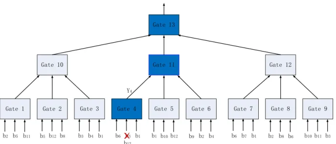
The classifier is based on binary data and Boolean circuits. More specifically, the classifier generated by the machine learning algorithm has the form of Boolean circuits, the inputs of the classifier are fixed length binary vectors, and the outputs are bits with each one corresponding to each classification outcome. The circuit takes the form of a tree (see Figure 4).
Gate 1 Gate 2 Gate 3 Gate 4 Gate 5 Gate 6
Gate 10 Gate 11
Gate 13
Gate 7 Gate 8 Gate 9 Gate 12
b2 b5 b11 b5 b12 b8 b3 b4 b1 b6 b3 b1 b1 b10b12 b9 b2 b4 b6 b7 b1 b2 b8 b6 b10b11 b3
The circuits of the classifier can be seen as a tree with each node of the tree containing a logic gate, and the leaves of the tree connected to data bits. The data bits can be images, texts or anything else that has the form of a binary vector with a fixed length. We can see from the figure above that the depth of the classifier is 3, the arity of the gate is 3, and the tree is full and complete.
To determine a classifier, we need to specify the inputs of each gate, which may be bits from some locations of the input data vector or outputs of the other gates. Also, we need to give a truth table for each gate.
2.2 Learning algorithms
The strategy to train a classifier is as follows: Firstly, we let the leaves of the tree be bits from random positions of the input data vector. Figure 5 shows an input data vector with 6 bits ({b0, b2, b6, b120, b390, b1000}) connected to the leaves of the tree. Secondly, we specify a truth
table for each gate in a greedy way, which means that every gate is trying to output the right classification decision. Thirdly, once the gates at the bottom of the tree are trained, we know their outputs for each training example. Then we are able to compute the gates on the upper layer, and so on until all the gates are known.
Gate 1
{b0, b1, b2, b3, b4, b5, b6 ...b50,...b120,...b390...b1000,...} Input data vector
Figure 5: Leaves of the tree are connected to input data bits randomly
We define that a k-gate is a function, mapping k input bits to an output bit. Hence, the number of possible k-gate is 22𝑘.
8
Y = F(𝑥1,𝑥2), where F is the logic function, 𝑥1,𝑥2 are two input bits, and Y is the output.
Input 𝑥1 𝑥2 Output Y 00 F(0,0) 01 F(0,1) 10 F(1,0) 11 F(1,1)
Table 1: 2-gate example
We are able to calculate the number of possible functions for 2-gate. In Table 1, there are four possible inputs. For each input, e.g. 𝑥1 𝑥2 = 00, there are two possible outputs, either F(0,0) = 0 or F(0,0) = 1. Hence, the total number of possible functions is 2*2*2*2 = 16 = 222.
That is to say, there are 16 different gates, with each of whom is defined by a truth table of 4 bits.
If we do the same calculations for 3-gate, we get 256 different gates. In addition, for 4-gate, we will get 65536 different gates; for 8-4-gate, we will get a huge number,
1.15*1077different possible gates.
In our design, we use 6-gate to construct our classifier. That means we have 1.8*1019 different possible gates. Obviously, it is infeasible to find the best possible gate by trying all these possibilities. Instead, a greedy algorithm is utilized to efficiently specify the truth table for each gate. That is to say, if we specify an output for each input pattern, the computation times will be reduced from 226 to 26 for each gate.
The truth table for a Gate
Bit 0 Bit 1 Bit 2 Bit 3 Bit 4 Bit 5 Output
Case 0 0 0 0 0 0 0 Positive (1)
Case 1 0 0 0 0 0 1 Positive (1)
Case 3 0 0 0 0 1 1 Positive (1) ……
Case 63 1 1 1 1 1 1 Negative (0)
Table 2: An example of building the truth table for a Gate
Table 2 shows a truth table for a gate. We use labeled data to train the Gate so that we are able to specify an output for each case of the input pattern. As the Gate has 6 inputs, it has 64 cases of input patterns. Two counters are used to decide the output for each input pattern. For example, when the input pattern of the Gate is {0,0,0,0,0,1}, a counter is used to count the number of the positive training examples, and another counter is used to count the number of the negative examples. If there are more positive examples than negative examples, then in the truth table, the output for that input pattern is set to positive (Logic 1). After training with an adequate size of dataset, the truth table is built for the Gate.
This greedy algorithm is able to efficiently produce a good classifier; however, it is observed that the performance is highly dependent on the choices of leaves’ inputs. To find a better classifier, we need to try different patterns of the leaves’ inputs. Obviously, this brute force search for a better classifier is very time consuming and not an efficient way.
An optimized way to search for a better choice of input data bits for leaves of the tree is shown in Figure 6. The strategy is: choose an input of leaves randomly; replace it with another different input, which is also chosen randomly; re-compute the gates along the way from the modified leaf to the output of the root while keep the other leaves unchanged. If the new classifier is better, we continue to update another leaf, or we keep updating that leaf for a certain time until we get a better classifier.
10
Gate 1 Gate 2 Gate 3 Gate 4 Gate 5 Gate 6
Gate 10 Gate 11
Gate 13
Gate 7 Gate 8 Gate 9 Gate 12
Y4
b2 b5 b11 b5 b12 b8 b3 b4 b1 b6 b3 b1 b1 b10b12 b9 b2 b4 b6 b7 b1 b2 b8 b6 b10b11 b3 b12
2.3 Object detection
We aim to perform ultrafast object detections with eight classifiers on the FPGA to recognize digit 0 to digit 7. The reason why we implement eight classifiers in this project is that the routing wires in the FPGA are already congested when implementing eight classifiers. It takes extra hours to compile more than eight classifiers or sometimes it fails to compile the project. This limitation can be broken by using a FPGA with larger capacity.
We use MNIST [26] dataset of handwritten digits to train our classifiers. Right now for testing, we use images containing a simple array of distinct digits. Each digit has the size of 24x24 pixels. Hence the sliding window we use has that size. The sliding window searches for all the subwindows in the image. The classification results will be output on every subwindow. Figure 7 shows the image with handwritten 0s and a sliding window appearing at the first and the last location.
12
Chapter 3 - Hardware architecture
Xilinx FPGAs provide high gate densities, rich on-board architectural features and multiple I/0 standards and the ability to be reprogrammed at any time [27]. These design advantages encourage us to shift the algorithms from the software to the FPGA hardware. By applying FPGAs technologies, a speedup by a factor of 3 orders of magnitude is expected in classification compared to the software solution.
Figure 8 describes the architecture of this project. The software on a desktop computer feeds images to the FPGA, and the FPGA returns the classification results to the software.
image …… image
results …… results
software
PC FPGA
Classifiers
Figure 8: High-level architecture and data flow between the PC and FPGA
3.1 FPGA design
In this project, we aim to implement multiple classifiers on a single FPGA, and process high-definition (1280x720) images at a speed of 60 frames per second. More specifically, inputs of our hardware platform are black and white images with each pixel encoded by one bit; classifiers are 5-level tree-constructed circuits; the sliding window has the size of 24 by 24 pixels.
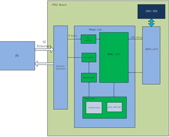
Our detailed FPGA architecture is shown in Figure 9. The FPGA Board is connected to a desktop computer via 1Gbps (bit per second) Ethernet. In our design, images are encapsulated into the payload field of Ethernet frames by the software in computer, and then fed to FPGA. In the FPGA, the Ethernet Interface block, which is an IP (Intellectual Property) core provided by Xilinx, is implemented to process the Ethernet communication with the computer. The
outputs of the Ethernet Interface are Ethernet frames which are sequentially buffered in the
Rx_buffer block, waiting for the memory control block (Memc_intf block) to move them to an
off-chip memory. When there is at least one image stored in the off-chip memory, the memory control block starts reading data from the off-chip memory and transfer them to the image processing block (Image_proc block), where a sliding window is implemented. The outputs of sliding window are subwindows (size of 24 by 24 pixels) of the image which are fed to the
classifiers block to do object detection. The classification results are sent to the results
buffering block (Result_buf block), and then encapsulated into Ethernet frames by the Ethernet transmission block (Tx_buffer block).
Image_top Memc_intf ddr3_ctrl DDR3 MEM Image_proc classifiers Rx_ buffer Ethernet Interface PC 1G Ethernet FPGA Board post_ddr_buf Tx_buffer Result_buf 8 bits 512 bits
Figure 9: FPGA architecture containing all the main blocks
We utilize Xilinx KC705 FPGA Evaluation Kit to implement our design. The evaluation board provides a high end FPGA chip (Kintex-7 XC7K325T-2FFG900C), a DDR3 SODIMM memory, a tri-mode Ethernet PHY and other features that are commonly used in an embedded system, as shown in Figure 10 [28].
14
Figure 10: Block Description of KC705 FPGA Evaluation Board [28]
3.2 Ethernet interface
In our design, we implement in the FPGA the Ethernet Medium Access Controller (MAC) which is responsible for the Ethernet framing protocols and error detection defined in IEEE 802.3-2008 specification. Figure 11 [29] illustrates that the Ethernet MAC locates in the Data Link layer of the OSI reference model. Meanwhile, our FPGA design is working on the MAC-control layer, which also belongs to the Data Link layer.
Figure 11: OSI reference model [29]
Our image data is encapsulated in Ethernet frames (Figure 12 [30]). The bytes within the frames are transmitted from left to right. The preamble field contains seven bytes of 0x55 which are used for synchronization. The Start of Frame Delimiter field determines the start of the frame with one byte 0xD5. The Destination Address field is filled with the MAC address of the intended recipient on the network. Likewise, the Source Address field is provided for the MAC address of the frame initiator. The Len/Type field is used as a length field when the two-byte value is less than 1536 (decimal); otherwise it is used as a type field. The Len field represents the number of bytes in the Data field while the Type field indicates which protocol is encapsulated in the payload of the frame. For example, 0x8100 indicates that the frame is a VLAN frame, and 0x8808 indicates a PAUSE MAC control frame. The Data field contains the user data which ranges from 0 to 1500 bytes. The Pad field is applied when there are less than 46 bytes in Data field to guarantee that the frame has at least 64 bytes. At the end of the frame, a 32-bit CRC value is calculated and filled in FCS (Frame Check Sequence) field.
16
In our design, to maximize the efficiency of the Ethernet transmission, we encapsulate 1440 bytes of the image data into the Ethernet frame, which contains 9 rows of data in a 720P image. In addition, we add 4 bytes to Data field to number the images and their rows. Hence, counting from the Destination Address to FCS, there are 6+6+2+4+1440+4 = 1462 bytes in every Ethernet frame.
As each Ethernet frame contains 9 rows of data in one image, it needs 80 frames to transfer a 720P image. For the 1Gbps Ethernet, taking into account the Preamble and SFD fields, the maximum number of images that can be transferred in one second is:
1Gbit
1470 × 8 × 80= 1062
PC EthernetPHY EthernetMAC FIFOs ...
Ethernet Interface
RGMII
Figure 13: Ethernet Interface in FPGA containing MAC and FIFOs
Figure 13 shows that there is an integrated Gigabit Ethernet Transceiver (Ethernet PHY) on the FPGA board to implement the physical layer communication between the FPGA and PC, and the interface between the Transceiver and FPGA is RGMII (Reduced Gigabit Media Independent Interface).
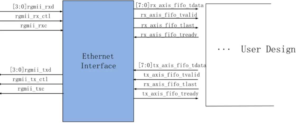
Ethernet Interface [7:0]rx_axis_fifo_tdata rx_axis_fifo_tvalid rx_axis_fifo_tlast rx_axis_fifo_tready [7:0]tx_axis_fifo_tdata tx_axis_fifo_tvalid rx_axis_fifo_tlast tx_axis_fifo_tready [3:0]rgmii_txd rgmii_tx_ctl rgmii_txc [3:0]rgmii_rxd rgmii_rx_ctl rgmii_rxc ... User Design
Figure 14: Input and output signals of Ethernet Interface block
Figure 14 shows the input and output signals of the Ethernet Interface block in our FPGA design. Signals on the left side are physical layer interface (RGMII) signals, and those on the other side are user signals that are used by designers to implement their applications.
The main signals in the reception side of the FPGA are explained as follows. The "rgmii_rxc" signal is the 125MHz clock sampling the receiving data –"rgmii_rxd" – at both rising edge and falling edge. The outputs of the block include an 8-bit data bus, a signal indicating the valid data and a signal indicating the end of an Ethernet frame.
3.3 External memory
In our design, an external memory is required to buffer the image data. The FPGA evaluation board provides a double data rate synchronous dynamic random access memory (DDR3 SDRAM) which achieves up to 1600 Mega transfers per second data rate [28]. We use CORE Generator tool provided by Xilinx to generate a DDR3 SDRAM memory interface, and we adapt the generated memory interface to fit our design.
The memory interface core is shown in Figure 15 [31]. The leftmost block is the User
Design block where designers implement their designs. This block is connected to the memory
controller through the User Interface. The following block is the User Interface Block which presents the user interface to the User Design block, as well as a flat address space and buffer read /write data path. The interface between User Interface Block and Memory Controller is the Native interface. It provides the way to send read/write requests and move data from the
18
User Design to external memory device. The Memory Controller presents the Native Interface
to User Interface Block and connects to the Physical Interface. The Physical Layer map the
Memory Controller Interface signals to Physical Interface signals which are connected to
external memory devices. It generates the signal timing and sequencing required to interface to external memory devices.
Figure 15: Memory Interface Core Architecture [31]
As depicted in Figure 16, in our system, the Memc_intf block is implemented as the User
Design block. It moves the Ethernet data from the Rx_buffer block to the DDR3 SDRAM. It
also adapts the 8-bit data from the Rx_buffer block to 512-bit data. The flow control mechanism is also included in the Memc_intf block by responding to the "post_ddr_ram_full" signal from the post_ddr_buf block (refer to Figure 9). More specifically, if the RAM in
post_ddr_buf block reaches its limit to buffer the data, it enables the "post_ddr_ram_full"
signal so that the upper block stops feeding data to it. In our design, the external memory is not expected to get overflowed as our hardware architecture is fast enough to process the data stream.
Memc_intf (User Design) init_calib_complete app_rdy app_wdf_rdy [511:0]app_rd_data app_rd_data_valid app_rd_data_end [7:0]rx_axis_tdata rx_axis_tvalid rx_axis_tlast pkt_ready [27:0]app_addr [2:0]app_cmd app_en [511:0]app_wdf_data app_wdf_wren app_wdf_end Rx_ buffer rd_addr_buf post_ddr_ram_full
Figure 16: User Design block for data transmission between FPGA and external memory
3.4 Sliding window
To search for all the subwindows with the size of 24 by 24 pixels, a sliding window is implemented in the FPGA. We combine a group of regular shift registers and RAM-based shift registers to construct the sliding window. In Figure 17, a 24-bit regular shift register and a 1256-bit RAM-based shift register are combined to buffer one row of image data. As the data in RAM-based shift registers is invisible, we use regular shift registers to output the subwindow’s data to classifiers. The reason why we use RAM-based shift registers is that they are formed by using the SRL16/SRL32 mode of the slice LUTs, which can improve the performance and lead to space savings [32]. The adjacent rows are connected end to end as shown below.
20
Regular shift registers RAM-based shift registers
Figure 17: The sliding window constructed by Regular shift registers from different rows Figure 18 illustrates how to represent a sliding window by moving the data along a group of shift registers. The example has a 7×7 pixel image and a 3×3 pixel sliding window. In the example, we only need to use three regular shift registers and three RAM-based shift registers. The first subwindow in original image contains the pixels: {1, 2, 3, 8, 9, 10, 15, 16, 17}. In order to get the first subwindow’s pixels, we shift the image data to the registers till the pixel 1 arrives at the end of the last regular register, which is shown on the top right in the figure. At this moment, we can have the first subwindow by reordering the pixels in the three regular shift registers. The second subwindow should contain the pixels: {2, 3, 4, 9, 10, 11, 16, 17, 18} as shown in the middle of the original image. In our design, as the image data continues right shifting by one position, we get the pixels of the second subwindow in the three regular shift registers, and again we need to reorder it. Hence, keeping right shifting the image data, we can get all the subwindows from the regular shift registers.
Figure 18: Description of how to get a subwindow by shifting data between shift registers
3.5 Classifiers
We implement in a single FPGA up to 8 independent binary classifiers. Each of them has 5 levels constructed by 1555 gates, and each gate has 6 inputs. We use an LUT6 (6-input look-up table) to implement a single gate. And the gates on different levels are connected by wire resources provided by the FPGA fabric. For all the classifiers, their leaves (input bits) are connected to pixels coming from the sliding window, and their outputs are encapsulated into Ethernet frames and sent to the PC. Figure 19 describes a group of independent classifiers implemented in our system.
Classifier#1 Classifier#2 Classifier#3
……
Classifier#8Sliding window
Figure 19: Data from the sliding window are fed to independent classifiers in parallel
1 2 3 4 5 6 7 17 16 15 14 13 12 11 8 9 10 11 12 13 14 10 9 8 7 6 5 4 15 16 17 18 19 20 21 3 2 1 22 23 24 25 26 27 28 29 30 31 32 33 34 35 36 37 38 39 40 41 42 43 44 45 46 47 48 49 1 2 3 4 5 6 7 18 17 16 15 14 13 12 8 9 10 11 12 13 14 11 10 9 8 7 6 5 15 16 17 18 19 20 21 4 3 2 1 22 23 24 25 26 27 28 29 30 31 32 33 34 35 36 37 38 39 40 41 42 43 44 45 46 47 48 49 1 2 3 4 5 6 7 19 18 17 16 15 14 13 8 9 10 11 12 13 14 12 11 10 9 8 7 6 15 16 17 18 19 20 21 5 4 3 2 1 22 23 24 25 26 27 28 29 30 31 32 33 34 35 36 37 38 39 40 41 42 43 44 45 46 47 48 49
22
Chapter 4 – Timing design
For any FPGA design, timing is the most important issue that designers must address, so we will introduce our timing design in detail. The description of the timing design in the FPGA can be divided into four parts. The first part explains how to receive and send Ethernet frames obeying the Ethernet framing protocols. The second part talks about buffering the received Ethernet frames in an on-chip memory before moving them to the external memory. The third part illustrates how a scheduling mechanism is designed to store the coming images into the external memory and read the stored images out of the external memory to feed to the next module. The last part mainly describes the timing of classification and the results buffering.
4.1 Ethernet frame reception and transmission
We implement a 1Gbps Ethernet interface by utilizing an IP CORE provided by Xilinx. In this chapter, we illustrate the design of the Ethernet interface.
Figure 20 describes the interface between the Ethernet MAC block and the FIFOs block. It is the AXI4-stream interface [33] that provides a data path for receiving and transmitting Ethernet frames.
Figure 21 shows the timing of a frame reception of the AXI4-stream interface at the speed of 1Gbps. All the signals in the receiver are synchronous to the clock signal: rx_mac_clk. Rx_axis_mac_tvalid is asserted when the output data is valid. When a frame reception has completed, rx_axis_mac_tlast will be asserted at the last frame cycle. If there is any error in the frame, rx_axis_mac_user will be asserted along with rx_axis_mac_tlast.
Figure 22 illustrates the timing of a frame transmission of the AXI4-stream interface at the speed of 1Gbps. Almost all the signals of the transmitter work in the same way as their counterparts in the receiver except the "ready" signal which is absent in the receiver. As the reception data path can’t be held off, there is no "ready" signal in the receiver to throttle the data. However, in the transmitter, the Ethernet MAC block is able to throttle transmitting data by de-asserting the tx_axis_mac_tready signal.
The FIFOs block provides the AXI4-stream user interface to User Design blocks (refer to Figure 14), and it contains FIFO components for both the transmitter and the receiver.
Ethernet
MAC FIFOs
Ethernet Interface
RGMII AXI4-stream AXI4-stream
Figure 20: AXI4-stream interface implemented in Ethernet Interface
Figure 21: Frame reception of AXI4-Stream interface at 1Gbps
Figure 22: Frame transmission of AXI4-Stream interface at 1Gbps
4.2 Data buffer between receiver and DDR3 memory
Although there is a frame reception buffer in the FIFOs block, we need another buffer to act as a bridge between the Ethernet receiver and the external memory controller. Hence, the
24
frame and buffer the Data field’s data in the on-chip memory (RAM). A finite state machine (FSM) is utilized.
As depicted in Figure 23, a FSM with six states is implemented. The FSM starts at the WR_IDLE state, waiting for the preceding FIFO to assert the "ready" signal. The FSM jumps to the PRE_WR state if the preceding FIFO is ready to output a frame. At the PRE_WR state, the DA and LT fields of the output frame are checked. If the frame is not wanted according to the DA and LT fields, the FSM goes to the BYPASS_DATA state to ignore the whole frame. Otherwise, it goes to the WR_DATA state to write the payload data to the RAM. At the WR_DATA state, if the RAM is full, the FSM jumps to the WR_RAM_FULL state and stays there until the RAM is not full. When the last byte of a frame is written into the RAM at the WR_DATA state, the FSM goes to the WR_EOF state. At the WR_EOF state, if the preceding FIFO has another frame ready, the FSM goes to the PRE_WR state to get the frame, or the FSM returns to its original state – the WR_IDLE state.
WR_IDLE PRE_WR WR_DATA BYPASS_ DATA WR_EOF Rece ive FIFO is read y Bypa ss t he f rame En d of a f ra me RAM is f ull Write to RAM R e c e i v e F I F O i s r e a d y No f rame i n FI FOs WR_RAM_ FULL RAM is n ot f ull End of a fra me
Figure 24 shows the timing of writing a frame to the RAM. In the figure, wr_en is the enabling signal of writing data to the RAM, and wr_addr is the address. cnt_pkt is the counter for the bytes of the frame.
Figure 24: Write a frame to the RAM
As depicted in Figure 25, the RAM is an asynchronous RAM with the writing signals working at the clock domain of 125MHz (for 1Gbps Ethernet) and the reading signals working at the clock domain of 200MHz (for DDR3 memory). Hence, some techniques are utilized to avoid the metastable problem in the clock domain crossing design.
Rx_buffer
clkb addrb clka addra dina wea doutbFigure 25: An asynchronous RAM
The metastable problem is illustrated in Figure 26. When the Setup and Hold time of a flip-flop is violated, the flip-flop output hovers at a value between the high level and the low
26
level for some period of time. If the metastable signal does not resolve to a low or high level before it reaches the next register, it can cause a logic to fail as different destination registers capture different values from the signal [34].
In the following example [35], the transition of the output of the Launch FF happens very close to the active edge of the clock of the Capture FF1, which leads to the metastable state in the Capture FF1. As it is a bi-stable device, the Capture FF1 may output either logic "0" or logic "1". Figure 27 shows a longer time of metastable state in the Capture FF1 than Figure 26. Hence, there is an uncertainty of when the metastable state vanishes. However, the probability that a flip-flop stays in the metastable state decreases exponentially with time [36]. A circuit known as a synchronizer is often used to allow sufficient time for the oscillation to settle down and to ensure (at a very high percentage) that a stable output is obtained in the destination domain. In fact, the Capture FF1 and the Capture FF2 is a multi-flop synchronizer which is commonly used.
Figure 27: Metastable state (2) [35]
In our design, when a frame is written to the RAM under the 125MHz clock domain, the wr_done2rd signal is sent across its clock domain to the 200MHz clock domain, which is shown in Figure 28. A two-flop synchronizer is implemented to synchronize the wr_done2rd signal to the 200MHz clock domain.
28
4.3 External memory user design
The Xilinx memory interface IP CORE provides a simple interface (User Interface) to the user design for communicating with the memory controller. Signals between the user design and the IP CORE is shown in Figure 15 (refer to 3.3 External memory). To perform Read/Write operations, designers should handle the signals of command path and read/write data path.
4.3.1 Command path
The signals of command path are listed in Table 3:
Signal Description
app_addr Address for the current request.
app_cmd Command for the current request
(read/write)
app_en Active-high strobe for the command
and address
app_rdy Indicates that the UI is ready to accept
commands Table 3: Signals of command path
To send a valid command, the app_addr, app_cmd and app_en should be sent together with the asserted app_en. When the app_rdy is asserted by the IP CORE, the command is accepted and written to the FIFOs in the IP CORE. Therefore, the user design needs to hold the app_en high along with the valid command and address values until the app_rdy is asserted. This is explained in Figure 29 [31].
Figure 29: Command path timing [31]
4.3.2 Write data path
The signals of write data path are listed in Table 41:
Signal Description
app_wdf_data Data for writing commands
app_wdf_wren Active-high strobe for App_wdf_data
app_wdf_end Indicates the end of the 512 bit data burst
app_wdf_rdy Indicates that the write data FIFO is ready to receive data
Table 4: Signals of write data path
To write data to the memory controller, there are two modes that we can choose. One is to write data back-to-back, in which case the writing commands are issued back-to-back and
30
the writing data can be presented before or after the writing commands for any clock cycles. The other mode is single writing. In this case, the maximum delay between the writing command and the associated writing data is two clock cycles. In our design, we choose the second mode, which is described in Figure 30.
Figure 30: timing of a single write operation [31]
4.3.3 Read data path
The signals of read data path are listed in Table 5:
Signal Description
app_rd_data Data output from memory controller
app_rd_data_valid Active-high output indicates that the app_rd_data is valid
app_wdf_end Active-high output indicates the last cycle of output data
Table 5: Signals of read data path
In Figure 31, the read data is returned with some latency by the memory controller, and it is always in the same order as the addresses are sent on the command path.
Figure 31: Timing of two reading operations [31]
4.1.3.4 FSM for read/write management
A FSM is implemented to manage memory read/write operations as shown in Figure 32. At the beginning, the FSM stays at the IDLE state until it is indicated that the preceding RAM has one row of image data ready for transferring. Then it goes to the WR_DATA state. When one row of image data has been transferred to DDR3, the FSM returns to the IDLE state and then checks if there is another row of image data to transfer. The FSM keeps moving data from the RAM to the DDR3 until there is an entire image in the external memory. Then the FSM goes to the READ_DATA state. At this state, if the post-DDR3 RAM is full, the FSM should jump to the RAM_FULL state and wait until the post-DDR3 RAM has enough space available. Then the FSM goes back to the READ_DATA state. In this state, when one row of image data has been read from DDR3, the FSM returns to the IDLE state. The IDLE state gives higher priority to transferring data to the DDR3 than reading data from the DDR3.
32 IDLE WR_DATA RD_DATA RAM_FULL The prec edin g RAM is r eady
One image is written and the preceding RAM is not
ready Havi ng w ritt en o ne ro w of i mage is do ne The post -DDR 3 RAM is f ull Th e po st -DDR 3 RA M is n ot f ull
Having read one row of image from DDR3 is done
Figure 32: FSM for read/write management
4.4 Image processing
Figure 9 in Chapter 3 shows that image processing block includes two blocks: one is the
post_ddr_buf block which buffers the data read from DDR3. The other block is the classifiers
block which includes multiple classifiers to do classification jobs.
4.4.1 Data loss problem in the asynchronous RAM
Although the function of the post_ddr_buf block is simple, we need to be careful with its timing design as it implements an asynchronous RAM. The Write Port of the RAM is running at the 200MHz clock domain while the Read Port is running at the 125MHz clock domain.
In section 4.1.2, we explain the metastable problem that may happen in an asynchronous digital design. In fact, there is another problem called data loss problem that may happen in that case. Figure 33 illustrates how to fix this problem in the post_ddr_buf block where an asynchronous RAM is implemented. The wr_en_done signal is asserted when every five data
have been written to the RAM, and it will be transferred to the Read Port to indicate that the RAM can be read. As the sampling clock in the Read Port is slower than that in the Write Port, the Read Port may miss the wr_en_done signal, which causes the data loss problem. In order to avoid this problem, the wr_en_done signal is extended by one clock to ensure that it can be sampled by the 125MHz clock. Meanwhile, a two-flop synchronizer is implemented to avoid the metastable problem.
Figure 33: Avoid data loss problem in asynchronous digital design
4.4.2 Subwindow's data
The data read from the asynchronous RAM in the post_ddr_buf block are 512-bit data, and they will be serialized to 1-bit data and then fed to shift registers. In Figure 34, the data4sr signal is the 1-bit data fed to shift registers, and the data4sr_valid signal indicates that the data4sr is valid. In addition, there are 24 registers (from sreg_1 to sreg_24) called regular shift registers, each of which is a 24-bit data bus (refer to Figure 17). In Figure 35, we can see that the delay between the sreg_1 and sreg_2 is 10240 ns, which equals to 1280 clock cycles.
In order to obtain the subwindow's data that will be transferred to classifiers, we can simply combine the 24 regular shift registers to form a long vector, as shown below in Verilog language.
assign classifier_data_in =
34
,sreg_13,sreg_14,sreg_15,sreg_16,sreg_17,sreg_18,sreg_19,sreg_20,sreg_21,sreg_22,sreg_ 23,sreg_24};
Figure 34: Data flow of Shift registers (1)
4.4.3 Classification and results buffering
The classifiers are tree-structure circuits with each node represented by a 6-input LUT. And they output a classification result at each clock cycle. All the classifiers are independent circuits working simultaneously. Figure 36 shows an example of two classifiers.
The classification results are buffered in the result_buf block (refer to Chapter 3 - Hardware architecture). A synchronous RAM is implemented in the result_buf block. When the sliding window moves along the rows from left to right, it traverses 1257 subwindows. Hence, as long as the RAM has buffered 1257 results, it tells the tx_buf block to encapsulate them to a single Ethernet frame. To traverse the whole image, the sliding window needs to move along 697 rows of the image, so the classification results of an image are contained in 697 Ethernet frames.
36
Chapter 5 – Evaluation
5.1 System Simulation
Creating a comprehensive simulation environment is an efficient way to debug the design. Although it is time consuming to build a simulation environment for an FPGA design, it actually saves a large amount of time for the in-circuit FPGA debug. There are three reasons that account for that. Firstly, it is quite difficult to locate an error when the FPGA program is running. Secondly, every time when the source code is modified, it often takes hours to re-compile a medium-scale FPGA project. Thirdly, during the simulation, errors can be seen clearly on the waveform and there are many ways to export the error information.
To verify our FPGA design, we build a simulation environment using the architecture of
testbench. The testbench is the top-level module in the simulation which is responsible for
stitching all the modules together. [37]
A testbench shown in Figure 37 is implemented to verify the correctness of our design. The DUT module is the synthesizable code that will be programmed to the FPGA. The Clocks and Resets module play the roles of the clock and reset signals in the evaluation board. The
DDR3 Model is the simulation component provided by Xilinx. The modules of Testcase, DataGen and BFM (Bus functional models) act as the software on PC. The Testcase module
defines the specifications of the data to send so that the DataGen module can generate the data accordingly. The BFM module provides an interface following the timing of a certain bus protocol. More specifically, in our design, the BFM module is defined as tasks to send and receive data according to the timing of the Ethernet framing protocol. In addition, to view simulation results, we write them to a log file.
From the simulation waveforms and log files, we verify that the project functions properly as what we design.
DUT (Device Under Test) Clocks Resets DataGen BFM Log Testbench Testcase DDR3 Model BFM
Figure 37 Testbench for system simulation
5.2 Functional verification
The success of the FPGA simulation doesn’t mean the program is error-free when running on the real hardware. Often, there will be unexpected problems.
To verify the functional correctness of our FPGA design on the evaluation board, we build a software-hardware system as shown in Figure 38. The software in PC is responsible for sending images to the FPGA board and displaying classification results collected from the FPGA. The software program is running on Win 7 OS, Intel Core i7 CPU @ 2.4GHz. In the program, WinPcap [38] [39] is utilized to send and receive packets via network, and OpenCV [40] is utilized to do image processing.
image …… image
FPGA
results …… results DisplayPC
Send image38
Start
Open Network Adapter Read an image from Disk Convert to black&white imageSend images via Ethernet
Receive results
Process results & Display
End
Figure 39: Software flowchart
Figure 39 describes the flow of the software. The images sent to the FPGA contain hand-written digits. For example, Figure 40 shows an image of handhand-written 0s that is transferred to the FPGA. Meanwhile, one of the classifiers in the FPGA has been trained to detect the 0s. To verify the FPGA design, we let the software send the same image repeatedly. When the software receives the Ethernet frames that contain the classification results, it extracts the results produced by the classifier that is trained to recognize 0s. Figure 41 gives an example of the Ethernet frames received by the software. In the DATA field of the Ethernet frame (refer to Chapter 3, 3.2 Ethernet interface), there are 1257 bytes (from D0 to D1257) that carry the classification results of eight classifiers. In this example, the lowest bit in each byte, such as c0 in D0, is the output of the classifier trained to detect digit 0. If the classifier outputs 0, it indicates that a digit is detected. We train the classifiers by images with the size of 24x24 pixels containing a digit right in the center. So theoretically, when the sliding contains a digit in the center, the digit will be detected. In the experiment, the sliding window starts at the left top of the image, and ends at the right bottom of the image. The classification results form an
image of 1257x797 pixels. We use a filter to do the post-processing for the classification results. The filter computes for each pixel the average pixel value of the neighboring pixels at maximum distance of 3 (Manhattan Distance), and then multiply the value by 3. Then we overlap the image of results on the evaluated image, with their top and left margins get aligned. A part of the overlapped image is shown in Figure 42. The ideal position of the red dots is on the left top of the digit. It can be seen that most of the digits are properly detected, although there are also some false positives.
Figure 40: Image of handwritten digits
DA SA Len/Type Frame Counter Image Counter D0 ={c7,c6,c5,c4,c3,c2,c1,c0} D1 D2 ... D1256
40
Figure 42: Results in the image (red marks are off-center because they top-left align the original image)
5.3 FPGA evaluation
To evaluate the performance of the FPGA design, we analyze the device utilization and the classification speed of the FPGA.
The FPGA project is compiled by Xilinx ISE 14.6, and it costs around 1 hour to compile the whole project. All the timing constraints are met during the compilation. The report of the device utilization is shown in Figure 43, which illustrates that the project consumes only a small portion of the FPGA Slice and RAM resources. The estimation of the on-chip power consumption is given by the ISE, as shown in Figure 44. We can see that the FPGA consumes the power of only 2.6W, which is much less than an Intel Core i3/i5/i7 processor that dissipates the power of at least 35W. Figure 45 shows the overview of the routed wires in the FPGA. Although the project doesn’t use much Slice resources, the routing resources are highly occupied.
Figure 43: FPGA device utilization reported by ISE
Figure 44: On-chip power consumption
Figure 45: Routed wires viewed by FPGA Editor
Theoretically, the maximum number of images that our FPGA system can evaluate per second is 125, which is explained as follow. In our design, there are eight classifiers,each of
42
which outputs one bit of the classification result every clock cycle. That is to say that, in 1 Gbps Ethernet interface, the FPGA output 8 bits every clock cycle, so each classifier is able to run at the speed of 125Mbps in maximum. A black & white image of 720P format has around 1M pixels, so the FPGA is capable of classifying images at the speed of around 125 fps.
In an experiment, we use one thread to send 10000 images to the FPGA board, and use the other thread to receive the Ethernet frames from the FPGA board. We found that the Ethernet driver, WinPcap, receives the Ethernet frames at around 200Mbps maximum, which constrains the FPGA to run the classification process at only around 26 fps.
There is a second approach to determine the maximum classification speed of the FPGA. We run only one thread to send images as fast as possible, assuming that all the Ethernet frames sent by the FPGA can be received. We insert the ChipScope into the FPGA to check the number of the Ethernet frames that the FPGA has received and sent. In the experiments, the software sends a 720P image for 1 million times to the FPGA at different speeds. If the FPGA can’t process the images at that speed, the counter for the FPGA transmission will indicate data loss. Through experiments, we find that the FPGA is able to evaluate the images at the speed of 68 fps in maximum without any data loss. Figure 46 shows the running time and the average speed of sending images. Figure 47 shows the Ethernet frames counter for the receiver and transmitter of the FPGA. As illustrated in Chapter 3 (3.2 Ethernet interface) and Chapter 4 (4.4.3 Classification and results buffering), an image is encapsulated in 80 Ethernet frames by the software, and the classification results of an image are encapsulated in 697 Ethernet frames by the FPGA. The cnt_rx_row and cnt_tx_row in Figure 46 illustrate that the FPGA has received 1 million images and sent classification results of 1 million images.
Figure 46: The sending speed of software
Figure 47: Utilize ChipScope to track the registers
We also evaluate the speedup of our hardware architecture compared with the software solution. A direct software implementation in Python running on an Intel i7-3970x CPU, which doesn’t use an FPGA chip, is able to output approximately 300,000 evaluation results per second, while the FPGA output about 476,000,000 evaluation results. Therefore, we have a 1588x factor of speedup with our FPGA design.
44
Chapter 6 – Conclusion and future works
In this thesis, we present an FPGA-based hardware architecture for a novel classifier. In our architecture, the 720P high definition black and white images are fed to an FPGA, and the classification results are output at every clock cycle. We implement eight classifiers that are able to do classification jobs in parallel. We implement an Ethernet interface to transfer data between the FPGA and the PC at the speed of 1 Giga bits per second. In addition, we utilize an off-chip memory to buffer the data. The source codes are written in Verilog and compiled by Xilinx ISE tool. The compiled file is implemented on the Xilinx Kintex 7 FPGA. We have demonstrated that our FPGA implementation achieves the speed of 68 fps with 8 classifiers to evaluate all the subwindows of the 720P black and white images. The project consumes 3% Slice registers, 12% Slice LUTs and around 3% RAMs. The estimated on-chip power consumption is 2.6W. A speedup of 3 orders of magnitude is achieved compared with the un-optimized software implementation.
This work can be continued in the following directions:
1. The most efficient way to improve the performance of the image classification is to move time consuming computation tasks from the software to the FPGA. In the current implementation, the FPGA device has a lot of resources left, and the off-chip memory has 8 G bits memory space and at least 10Gbps data throughput [41], therefore we can implement the color space conversion and image scaling in the FPGA. In addition, we are now running the software on Windows OS to do post-processing of the classification results, which greatly limits the performance of the whole system. If the classification results are processed in the FPGA and displayed via the HDMI interface on the evaluation board, it will maximize the power of the FPGA.
2. Another improvement can be made on the interface between the FPGA and PC. In our current work, we use the 1 Gbps Ethernet interface to connect the FPGA and PC, which forms the bottleneck of the data bandwidth of the system. However, we can utilize the 10 Gbps Ethernet interface or the PCIe interface (10 Gbps) that have been
provided on the evaluation board. With higher data bandwidth, the FPGA is able to process images with higher definition.
3. The tree-structured classifier in this work has a depth-5 structure. If we use depth-6 classifiers, we can only implement two classifiers in the FPGA. This is because the routing becomes so congested that the Xilinx ISE software is unable to complete it. We can rebuild the project in a new development environment – Vivado IDE, which has a more advanced routing strategy. Moreover, an FPGA with a larger capacity could be used.
Bibliography
[1] Ron Kohavi; Foster Provost (1998). "Glossary of terms". Machine Learning 30: 271–274. [2] Dietterich, Thomas G. "Approximate statistical tests for comparing supervised
classification learning algorithms." Neural computation 10.7 (1998): 1895-1923.
[3] Chapelle, O., Schölkopf, B., Zien, A.: Semi-Supervised Learning. Adaptive computation and machine learning. MIT Press, Cambridge (2006)
[4] Kiritchenko, Svetlana, and Stan Matwin. "Email classification with
co-training." Proceedings of the 2011 Conference of the Center for Advanced Studies on Collaborative Research. IBM Corp., 2011.
[5] Basili, Roberto, Alessandro Moschitti, and Maria Teresa Pazienza. "NLP-driven IR: Evaluating performances over a text classification task."INTERNATIONAL JOINT CONFERENCE ON ARTIFICIAL INTELLIGENCE. Vol. 17. No. 1. LAWRENCE ERLBAUM ASSOCIATES LTD, 2001.
[6] I. Kononenko, Machine learning for medical diagnosis: history, state of the art and perspective, Artif. Intell. Med. 23 (2001) 89–109.
[7] Kotsiantis, Sotiris B., I. Zaharakis, and P. Pintelas. "Supervised machine learning: A review of classification techniques." (2007): 3-24.
[8] W. James MacLean, "An Evaluation of the Suitability of FPGAs for Embedded Vision Systems," IEEE CVPR 2005, pp.131.
[9] C. He, A. Papakonstantinou and D. Chen, "A Novel SoC Architecture on FPGA for Ultra FastFace Detection," ICCD 2009, pp.412-418, 4-7 Oct. 2009.
[10] C. Kyrkou, T. Theocharides, "A Flexible Parallel Hardware Architecture for AdaBoost-Based Real-Time Object Detection," IEEE TVLSI, vol.19, no.6, pp.1034-1047, 2011. [11] Haruyama, Shinichiro. "FPGA in the Software Radio." IEEE Communications Magazine (1999): 109.
[12] D. A. Buell, T. A. El-Ghazawi, K. Gaj, and V. V. Kindratenko, "Guest editors’
27, 2007.
[13] C. H. Zhiyong, L. Y.Pan, Z. Zeng and M.Q.-H Meng. "A Novel FPGA-Based Wireless Vision Sensor Node". Proc. of the IEEE International Conference on Automation and Logistics Shenyang, China August 2009.
[14] MCLEAN, M. AND MOORE, J. 2007. Securing FPGAS for red/black systems, FPGA-based single chip cryptographic solution. In Military Embedded Systems.
[15 ] S. Jin, J. Cho, X. D. Pham, K. M. Lee, S. K. Park, M. Kim, and J. W.Jeon, "FPGA design and implementation of a real-time stereo vision system," IEEE Trans. Circuits Syst. Video Technol., vol. 20, no. 1, pp.15–26, Jan. 2010
[16 ] C. Farabet, C. Poulet, J. Y. Han, and Y. LeCun, "Cnp: An fpga-based processor for convolutional networks," in International Conference on Field Programmable Logic and Applications, 2009.
[17] Z. K. Baker and V. K. Prasanna. Efficient hardware data mining with the Apriori algorithm on FPGAs. In Proceedings of the 13th IEEE Symposium on Field-Programmable Custom Computing Machines, pages 3–12, 2005.
[18] Ovtcharov, Kalin, et al. "Accelerating Deep Convolutional Neural Networks Using Specialized Hardware."
[19] J. Tarango, "Intermediate Embedded and Real-Time Systems", URL: http://www.cs.ucr.edu/~jtarango/cs122a_intro_to_fpgas.html
[20] Cosoroaba, Adrian, and Frédéric Rivoallon. "Achieving higher system performance with the Virtex-5 family of FPGAs." White Paper: Virtex-5 Family of FPGAs, Xilinx WP245 (v1. 1.1) (2006).
[21] B. Zahiri, "Structured ASICs: Opportunities and challenges," in Proc. Int. Conf. Computer Design, 2003, pp. 404–409.
[22] CANIS, A., CHOI, J., ALDHAM, M., ZHANG, V., KAMMOONA, A., ANDERSON, J., BROWN, S., AND CZAJKOWSKI, T. LegUp: High-level synthesis for FPGA-based
processor/accelerator systems. In Proceedings of the ACM International Symposium on Field Programmable Gate Arrays. 33–36. 2011.
![Figure 1: FPGA Architecture [19]](https://thumb-eu.123doks.com/thumbv2/123doknet/8151958.273663/12.918.245.707.577.876/figure-fpga-architecture.webp)
![Figure 3: FPGA Design Flow [24]](https://thumb-eu.123doks.com/thumbv2/123doknet/8151958.273663/14.918.159.716.331.728/figure-fpga-design-flow.webp)


![Figure 10: Block Description of KC705 FPGA Evaluation Board [28]](https://thumb-eu.123doks.com/thumbv2/123doknet/8151958.273663/24.918.220.732.121.519/figure-block-description-kc-fpga-evaluation-board.webp)
![Figure 11: OSI reference model [29]](https://thumb-eu.123doks.com/thumbv2/123doknet/8151958.273663/25.918.249.691.119.427/figure-osi-reference-model.webp)