Credit Authors Statement
B. Aspe: Conceptualization, Formal Analysis, Investigation, Writing – Original draft, Visualization
V. Demange: Conceptualization, Formal Analysis, Investigation, Supervision, Writing – Original Draft, Visualization, funding acquisition
A. Waroquet: Investigation, Resources
X. Castel: Conceptualization, Formal Analysis, Investigation, Supervision, Writing, Visualization, funding acquisition
B. Gautier: Conceptualization, Formal Analysis, Investigation, Writing, Visualization
Q. Simon: Conceptualization, Formal Analysis, Investigation, Writing, Visualization
D. Albertini: Formal Analysis, Investigation, Resources
M. Zaghrioui: Conceptualization, Formal Analysis, Investigation, Writing, Visualization
K. Nadaud: Conceptualization, Formal Analysis, Investigation, Writing, Visualization
S. Députier: Conceptualization, Investigation, Resources, Writing
F. Gouttefangeas: Formal Analysis, Investigation, Resources
R. Sauleau: Conceptualization, Formal Analysis, Investigation, Supervision, Writing, Visualization, funding acquisition
M. Guilloux-Viry: Conceptualization, Investigation, Supervision, Writing, Project Administration, funding acquisition
Tetragonal tungsten bronze phase thin films in the
K-Na-Nb-O system: pulsed laser deposition,
structural and dielectric characterizations
B. Aspea,b, V. Demangea,c, A. Waroqueta, X. Castelb, B. Gautierd, Q. Simone, D. Albertinid, M. Zaghriouie, K. Nadaude, S. Députiera, F. Gouttefangeasc, R. Sauleaub, M.
Guilloux-Virya,c
a
Univ Rennes, CNRS, ISCR – UMR 6226, F-35000 Rennes, France
b
Univ Rennes, CNRS, IETR – UMR 6164, F-35000 Rennes, France
c
Univ Rennes, CNRS, ScanMAT – UMS 2001 F-35000 Rennes, France
d
Univ Lyon, CNRS, UMR 5270, Inst Nanotechnol Lyon, Inst Natl Sci Appl Lyon, F-69621 Villeurbanne, France
e
GREMAN – UMR 7347, University of Tours, CNRS, INSA CVL , F-41000 Blois, France
Corresponding authors:
Maryline Guilloux-Viry: email address: maryline.guilloux-viry@univ-rennes1.fr ORCID identifier: 0000-0001-7773-1643
phone number: +33 (0) 2 23 23 56 55
Valérie Demange: email address: valerie.demange@univ-rennes1.fr ORCID identifier: 0000-0002-8153-2660
phone number: +33 (0) 2 23 23 67 88
Barthélemy Aspe: email address: barthelemy.aspe@univ-rennes1.fr ORCID identifier: 0000-0001-8927-4013
phone number: +33 (0) 2 23 23 65 70
ABSTRACT
Pulsed laser deposition parameters have been determined to synthesize pure Tetragonal Tungsten Bronze (TTB) phase thin films in the (K,Na)-Nb-O system (KNN). In relation to the
high volatility of alkaline elements, it was found that the target composition and the target-substrate distance are of first importance. The TTB phase was identified by X-ray and electron diffraction and the surface microstructure consisting mainly of nanorods supports the formation of hallmark of the TTB phase. Poly-oriented nanorods have been obtained on both C-plane sapphire and (111)Pt/TiO2/SiO2/(001)Si substrates whereas horizontal nanorods
oriented along the (hk0) planes have been grown on (100) and (110) SrTiO3. All the nanorods
are parallel together when grown on (110) SrTiO3 and they present two in-plane orientations
rotated of 90° from each other on (100) SrTiO3. Dielectric characteristics (dielectric
permittivity
ε
r, and loss tangent tanδ
) have been measured at low (1 kHz - 1 MHz) and high(1 GHz - 40 GHz) frequencies, on films deposited on Pt coated silicon and sapphire, respectively. A value of εr = 200 at 1 kHz with tan
δ
= 0.015 were measured in a parallel platecapacitor configuration, whereas εr = 130 and tan
δ
= 0.20 at 10 GHz were retrieved fromtransmission lines printed on the KNN TTB thin film grown on C-plane sapphire. Raman investigations of the TTB films were performed in the temperature range 77 - 873 K, confirming the TTB phase formation and the absence of structural transition. Piezoelectric Force Microscopy measurements evidenced a piezoelectric signal although no switching could be performed. However the dielectric measurements, complicated by high leakage currents when a DC voltage was applied, did not evidence any proof of ferroelectricity for the undoped KNN TTB films whereas results reported on other niobates (A,A')0.6Nb10O30 (with
560°C, separating the paraelectric phase (space group: P4/mbm N°127) and the ferroelectric one (space group: P4bm N°100).
1. INTRODUCTION
Ferroelectric and piezoelectric materials have a wide range of applications from sensors to micro-electro-mechanical systems (MEMS), memory devices and tunable devices, e.g. [1–3]. For decades, the PbZr1-xTixO3-based (PZT) material has been the most popular ferroelectric
materials [4]. Lately an effort has been made by the scientific community to find a more ecologic and less toxic alternative to this material. Since 2004, the KxNa1-xNbO3
perovskite-type material has been established to be a potential substitute for PZT due to its high piezoelectric coefficient d33 (up to 300 pC/N [5]) leading to an important investigation of this
phase [6, 7]. The KxNa1-xNbO3 perovskite phase has been investigated in bulk [8], thin films
[9], single crystals [10] and for photovoltaic applications [11], energy storage [12], luminescence properties [13], sensors [14] or medical imaging [15]. However, in the KNN system, many other phases of potential interest exist without being thoroughly investigated. In many chemical systems, such as K-Nb-O (KN), K-Ta-O, K-Li-Nb-O (KLN) or K-Ta-Nb-O, chemically close to the KNN system, Tetragonal Tungsten Bronze (TTB) phases have been reported either as thin films or bulk [16–20]. The TTB structure can be described along the [001] direction by two cationic octahedral sites B1 and B2 and three cationic tunnels A1, A2 and C, as presented in Figure 1. A1 and A2 sites can be occupied by alkaline metals, alkaline earth, rare-earth and a few other elements. B1 and B2 sites can mostly be occupied by small and highly charged cations, such as Nb5+, Ta5+ or W6+. Finally, the C sites can only be occupied by small cations and are often found to be empty.
Figure 1. Projection of the tetragonal tungsten bronze structure along the [001] direction showing the three cationic tunnels A1, A2, and C, and the cationic octahedral sites B1 and B2 [16].
Over the years this crystallographic structure with different cationic sites [21] which authorizes many cationic substitutions and doping possibilities was found to be of interest for exhibiting various properties. For example, in the KLN system, a TTB single crystal study has reported values of piezoelectric coefficient d33 equal to 52 pC/N and ferroelectric polarization
Pr of 25-30 µC/cm² [22]. Piezoelectric coefficients d33 were measured reaching 190 pC/N and
114 pC/N, for MnO2-doped and K-doped TTB ceramics in the Sr-Ca-Na-Nb-O system,
respectively [23, 24]. In the Sr-Ba-Na-Nb-O system, the TTB phase exhibits a relative permittivity as high as 1600 at 1 kHz [25]. This structure is also studied for optical properties [26] and catalytic activities [27]. In the KNN system, even though the TTB phase has been found as a secondary phase in bulk perovskite [28–30], the pure phase was neither reported nor properly characterized. Some previous works on a modified KxNa1-xNbO3 perovskite
ceramic have reported that the TTB phase, as a secondary phase, could explain the increase of the piezoelectric properties [29]. The presence of this secondary phase is related to an alkaline deficiency in the ceramic product. Indeed, the (K,Na)6Nb10O30 TTB phase is 40 % lower in
As no precise description of the KNN system exists when the alkaline/niobium ratio is less than 1, an analogy with the KN system, chemically close to the KNN system has to be made to obtain the TTB phase. In such a system however, various phases are shown to exist with different alkaline/niobium ratios making the pure TTB phase hard to obtain. Nonetheless, the pulsed laser deposition (PLD) technique is suitable for this type of investigation. Indeed, if the method is known to be congruent in the absence of volatile cation, it offers also a great possibility to tune the composition of the films, either by the modification of the target one and/or by the modification of the deposition parameters. Therefore because of the high alkaline (especially potassium) volatility, a thorough investigation of the deposition parameters is requested to grow the pure phase [31].
In this work, KNN thin films were grown by pulsed laser deposition to control pure TTB phase. The films were deposited on different substrates, i.e. single crystals (100) and (110) SrTiO3, C-plane sapphire and (111)Pt/TiO2/SiO2/(001)Si. SrTiO3 was used here to control the
orientation while C-plane sapphire and (111)Pt/TiO2/SiO2/(001)Si were used to provide
suitable samples for physical measurements. A particular attention was paid to the influence of the deposition parameters on the composition and the structure of the films.
The morphology, structural features and composition have been first investigated using scanning electron microscopy (SEM), X-ray diffraction (XRD), transmission electron microscopy (TEM), Raman spectroscopy and energy-dispersive X-ray spectroscopy (EDXS) analyses. In addition, dielectric properties (relative permittivity and intrinsic loss tangent) have been measured at low (from 1 kHz to 1 MHz) and high (from 1 GHz to 40 GHz) frequencies.
2.1. Elaboration of the KNN targets
The ceramic targets were prepared from KNN powders synthesized by solid state reaction at 940°C for 4 hours in air, from sodium carbonate Na2CO3 (RP NORMAPUR 99.8%),
anhydrous potassium carbonate K2CO3 (ACROS Organics 99%) and niobium oxide Nb2O5
(Alfa Aesar 99.5%) powders preliminary mixed in a planetary ball-mill and then calcined. Afterwards 25-mm in diameter targets were sintered either by conventional sintering at 1000°C for 12 h in air, or by Spark Plasma Sintering (SPS, FCT System GmbH). Indeed in the case of the deposition of the perovskite films, KNO3 enriched targets are used in order to
obtain the final alkaline/niobium ratio of 1. Because of its low melting point, the addition of KNO3 in the target favors its sintering [32]. This is not the case for the deposition of TTB thin
films which is performed through a non-enriched target. As the target density impacts the overall quality of the thin films and the droplet formation during deposition [33], the alternative SPS method has been used to enhance target density in comparison with targets obtained by conventional sintering. In that case, the powders are placed into a graphite mold which maintains the proper diameter. Graphite foils are introduced between the powder and the mold to facilitate the outmolding. By SPS, a one-step reactive sintering for 10 minutes at 1000°C and about 1 hour of cooling under a 1 bar argon atmosphere leads to a 25-mm-diameter dense KNN ceramic target of which the composition is given in Table 1. A cleaning process of the target of 5 hours at 900°C in air is required to remove the carbon film from the target surface. This step is also used for oxygenation of the ceramic targets. These parameters have been adapted from the work of M. Bah et al. [34] and preparation details of each target are summarized in Table 1.
Table 1. Chemical composition and sintering details of the different prepared targets. The accuracy of the composition values is 5 %. Target number Targeted composition Measured composition
Target T1 (K0.5Na0.5)NbO3 (K0.55Na0.45)0.93NbOx
Standard solid-state sintering at 1000°C for 12 h Target T2 (K0.5Na0.5)0.7NbO3 (K0.51Na0.49)0.68NbOx
Standard solid-state sintering at 1000°C for 12 h Target T3 (K0.5Na0.5)0.7NbO3 (K0.49Na0.51)0.54NbOx
Spark plasma sintering at 1000°C for 10 minutes
2.2. Elaboration of the KNN thin films by PLD
Thin films were deposited by PLD technique with a KrF excimer laser (Coherent company, pulse duration 20 ns, λ = 248 nm) sets at a fluence of 2-3 J cm-2, an energy of 210 mJ and currently at 2 or 4 Hz working frequency. Thin films have been deposited under 0.3 mbar oxygen pressure, at a deposition temperature in the range 600 – 650°C, with a target – substrate distance from 55 to 65 mm. In these conditions the deposition rate is close to 15 nm/min (at 2 Hz) and 30 nm/min (at 4 Hz). In this study the thickness of the films is typically between 250 and 500 nm.
2.3. Choice of the substrates
The films were grown on single crystals (100) and (110) SrTiO3, C-plane sapphire (i.e. (0001)
Al2O3) and (111)Pt/TiO2/SiO2/(001)Si from Crystal GmbH supplier. SrTiO3 (perovskite
structure with a dielectric permittivity
ε
r higher than 300) is a model substrate for the growthof oxides in view to control their orientation. Sapphire is suitable for high frequency applications thanks to its low dielectric permittivity and loss values (
ε
r≈ 10 and tanδ ≈ 10-4 at10 GHz and room temperature). For the fabrication of the microwave devices, the films have been deposited on 10 mm × 10 mm × 0.5 mm C-plane sapphire substrates. Finally Pt coated silicon (5 mm × 10 mm × 0.7 mm) is well adapted for dielectric measurements in parallel plate capacitor geometry. Each substrate was cleaned in acetone and isopropanol, prior to the deposition step.
The structural characteristics were investigated by X-ray diffraction (XRD) by using a
θ−2θ
diffractometer (D8 Advance, BRUKER) with a monochromatized Cu Kα1 wavelength (λ = 1.54056 Å). The surface morphology was observed by scanning electron microscopy (SEM, JSM 7100F, JEOL and MIRA3 Tescan) coupled with an energy dispersive X-ray spectroscopy detector (SEM-EDXS, SDD X-Max 50 mm2, Oxford Instruments) to determine the thin film composition. A 5 nm–thick carbon layer was deposited before SEM-EDXS analysis to ensure optimal element detection and especially the potassium one that we have observed to be highly sensitive to charge accumulation effect.Transmission electron microscopy (TEM) experiments were performed by using a LaB6 JEOL 2100 instrument equipped with an Oxford Aztec 80 mm2 SDD device for EDXS analysis (TEM-EDXS). Samples were prepared by scratching the thin film from the substrate with a diamond tip and by collecting the so-obtained particles on an amorphous carbon copper grid (Agar). Bright field and dark field transmission electron micrographs, and electron diffraction patterns were recorded using a GATAN Orius 200D CCD (charge coupled device) camera. Schemes of structures were drawn with CrystalMaker software from CIF files of phases under consideration. Simulations of electron diffraction patterns were obtained with the help of CrystalDiffract extension of CrystalMaker.
Raman measurements versus temperature (from 77 to 873 K) were performed on TTB-type KNN coated (111)Pt/TiO2/SiO2/(001)Si substrates using Renishaw Invia spectrometer and
temperature controller (Linkam THMS 600). A green line (514 nm) of Argon-ion laser was taken as the excitation source with a power lower than 1 mW to hedge again heating effect. The scattered light was collected by a ×50 objective and dispersed by 2400 lines/mm grating in the back-scattering configuration.
Piezoelectric Force Microscopy (PFM) images were obtained with a NTEGRA NT-MDT system using the so-called « Dual Frequency Resonant Tracking » mode, which enables to
enhance the signal to noise ratio by working near the contact resonance frequency of the tip-sample system. Platinum-Iridium tips have been used, with stiffness in the 2-10 N.m-1 range. In amplitude images, bright zones correspond to higher amplitudes of vibration.
The low frequency dielectric measurements were performed on parallel plate capacitors. Top Au electrodes of surface area S (∅ = 300 µm, thickness tAu = 200 nm) were deposited by
magnetron sputtering technique through shadow mask on KNN coated (111)Pt/TiO2/SiO2/(001)Si substrates. The capacitance C and the loss tangent (tanδ) were
measured at room temperature from 1 kHz to 1 MHz with an AC driving voltage Vac = 125
mV, using an Agilent 4294A impedancemeter. The dielectric permittivity
ε
r of each samplewas retrieved from the measured capacitance (C) using the parallel plate capacitor formula, where tKNN is the thickness of the KNN film:
ε
=
×ε × (1)
2.5. Microwave devices for dielectric characterization at microwave frequencies
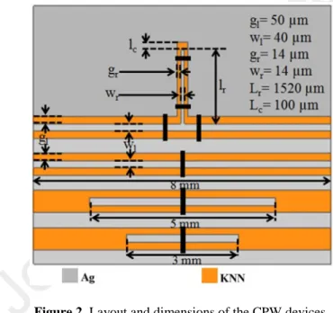
The dielectric characteristics and frequency tunability of the KNN TTB thin films were investigated using coplanar waveguide (CPW) and transmission lines devices designed with a 3-D commercial electromagnetic software (Ansys HFSSTM). Three 50-Ω lines (8 mm, 5 mm and 3 mm long) with a conductor width wl = 40 µ m surrounded by a gap gl = 50 µm (Figure 2)
were implemented to retrieve the thin films dielectric characteristics (
ε
r, tanδ), from themicrowave measurements. A CPW quarter-wavelength open-ended stub resonator was also designed to operate in X-band. Its resonance frequency Fr depends upon the stub length Lr and
the effective permittivity
ε
eff of the heterostructure, as follows:where c is the speed of light in vacuum. The devices were fabricated from a 2 µm-thick silver overlayer grown on a 5 nm-thick titanium underlayer deposited by RF magnetron sputtering at room temperature. The silver thickness is three times larger than the skin depth value (
δ
= 0.64 µm) at 10 GHz. Note that the ultrathin titanium film is used here only to ensure the strong adhesion of the silver film onto the ferroelectric oxide. Standard photolithography and wet etching processes were implemented to pattern the devices. Gold wire bondings (15 µm-diameter and 250 µm-length) were used to enforce the equipotential condition on both CPW grounds and prevent from the excitation of parasitic slotline mode (Figure 2).Figure 2. Layout and dimensions of the CPW devices.
Microwave measurements at room temperature and from 20°C to 240°C were carried out through a probe station coupled to a vector network analyzer (VectorSTAR MS4644B, ANRITSU) from 1 to 40 GHz under an external DC bias voltage range from 0 to 150 V, which corresponds to a maximal static electric field Ebias equal to 90 kV/cm for the stub
resonator and 27 kV/cm for the transmission lines. The measured gap dimensions (gr ≈ 16 µm
and gl ≈ 52 µm) are slightly larger than the nominal ones due to the inherent overetching of
3. RESULTS AND DISCUSSION
3.1. Influence of the deposition parameters to grow pure KNN TTB thin films on the various substrates
From a previous study [32] it has been shown that among the various deposition parameters, the target composition, the deposition temperature and the target – substrate distance D have a strong impact on the thin films composition and crystallization, explaining their accurate assessment impact. Table 2 gathers the deposition parameters of the films considered in the present study. Since a film thickness of about 250 nm was obtained with the laser frequency of 2 Hz, the frequency was increased to 4 Hz to achieve a thickness near 500 nm, more suitable for the high frequency reconfigurable devices [47].
The samples labelled in Table 2 are the most significant in view to control the TTB single phase in the KNN system.
Table 2. Summary of deposition parameters and different characteristics of the thin films. The accuracy of the composition values is 5 %.
Thin
film Substrate Target
Freq. (Hz) Temp. (°C) Dist. target-subs. (mm) Identified phase by XRD Measured composition (EDXS) F1 (110)SrTiO3 T1 2 600 55 Perovskite TEM (K0.4Na0.6)0.92NbOx F2 Nb:(110)SrTiO3 T1 2 650 55 Perovskite TEM (K0.14Na0.86)0.79NbOx F3 Nb:(110)SrTiO3 T2 2 600 55 TTB + K4Nb6O17 TEM (K0.58Na0.42)0.62NbOx F4 (110)SrTiO3 T3 4 650 65 TTB SEM (K0.45Na0.55)0.44NbOx F5 (001)SrTiO3 T3 4 650 65 TTB SEM (K0.47Na0.53)0.43NbOx
F6 (111)Pt/TiO2/SiO2/(001)Si T3 4 650 60
TTB + KNb3O8
SEM (K0.49Na0.51)0.46NbOx
F7 C-plane sapphire T3 4 650 65 TTB SEM (K0.49Na0.51)0.41NbOx
F8 C-plane sapphire T3 4 650 60 TTB SEM (K0.49Na0.51)0.40NbOx
F9 C-plane sapphire T3 4 650 55 TTB + KNb3O8
SEM (K0.50Na0.50)0.45NbOx
First the role of the target composition has been investigated. Since data have not been yet
reported on the TTB phase in the KNN system, the knowledge about the KN system [31] chemically close to the KNN one, has been therefore considered. With the aim to obtain a thin film composition close to (KxNa1-x)6Nb10O30 and while taking into account the alkaline
elements volatility during the PLD process [31, 32], the K0.5Na0.5NbO3 target (T1)has been
first used. As shown in Figure 3a, XRD pattern of the F1 film, grown on (110)SrTiO3 at
600°C, displays the K0.4Na0.6NbO3 perovskite phase peaks with a (101) preferential growth, in
agreement with the Joint Committee on Powder Diffraction Standards (JCPDS) file #00-061-0310 (space group: Pm (6); a = 3.99628 Å, b = 3.93776 Å, c = 3.99335 Å,
β
= 90.3398°). The SEM micrograph (Figure 3b) shows a F1 film made of crystallites with rectangular shape of about 300 nm × 100 nm, aligned in the plane along the <100> axis of the substrate. A few crystals (white contrast) with higher size are also observed. The composition determined by SEM-EDXS (K0.4Na0.6)0.92NbO3 is in good agreement with the XRD results and the expecteddepletion in alkaline elements, especially potassium, during the PLD process. Nevertheless, this depletion is not sufficient to achieve the composition range of the TTB phase.
Figure 3. XRD patterns of F1, F2, F3 films (#: K4Nb6O17 phase, *: substrate) (a). Scanning electron
micrographs of F1, F2 and F3 films (b-d).
A second film, namely F2, was grown on the Nb:(110)SrTiO3 from the same target at higher
temperature. The related composition is (K0.14Na0.86)0.79NbOx with a lower amount of alkaline
elements, but still too high for the expected composition. The depletion in potassium is particularly high in this sample. Among the several perovskite phases known in this part of the KxNa1-xNbO3 solid solution, only K0.1Na0.9NbO3 (JCPDS files # 01-074-2025, space
group: Pm (6); a = 7.8720 Å, 7.7920 Å, 7.8632 Å,
β
= 90.479°) fits with the XRD pattern, with a (101) preferential growth (Figure 3a). The SEM micrograph shows a film made of very long (several microns) and thin parallel crystallites (50-100 nm wide)(Figure 3c).To favor the growth of the TTB phase, the alkaline target composition was further decreased down to (K0.5Na0.5)0.7NbO3 (target T2). The film obtained at 600°C using this target (F3) leads
to the formation of the TTB phase on Nb:(110)SrTiO3 as displayed by XRD (Figure 3a). On
this pattern, only {hk0} peaks of the TTB phase are present indicating preferential growth according to the JCPDS file #01-087-1856 of the K6Nb10.88O30 TTB phase (space group: P4/mbm (127); a = 12.5820 Å, c = 3.9920 Å). A minor peak at 2θ = 14.54° indicates the presence of the K4Nb6O17 phase (JCPDS file #01-076-0977) as a secondary phase. The
corresponding SEM micrograph shows long (several microns) and thin crystallites (50 nm wide). Some other crystallites exhibit out-of-plane short nanorod shape (white contrast on the SEM micrograph). The (K0.58Na0.42)0.62NbOx composition is therefore close to the expected
one. Morphology of the F2 (perovskite phase) and F3 (TTB phase) films being very similar, further transmission electron microscopy and electron diffraction experiments were performed to get in-plane information.
Figure 4 presents bright field micrographs and electron diffraction patterns (EDP) along the normal of F1, F2 and F3 films. EDP of the (K0.4Na0.6)0.92NbO3 perovskite phase (film F1)
displays a primitive rectangular cell, which corresponds to the [101] zone axis of a pseudo-cubic cell with lattice parameters close to 4 Å (Figure 4b), as expected from the simulated EDP (Figure 4c). For the purpose of comparison, the (110) SrTiO3 cell was drawn in red in all
the EDPs of Figure 4.The perovskite phase presents therefore epitaxial relationships with the (110) SrTiO3 substrate, whose cell has roughly the same dimensions. The related relationships
are: [101]KNN//[101]STO, (010)KNN//(100)STO, (101)KNN//(101)STO. Comparison between image
and diffraction pattern enable to determine the elongation direction of the small rectangular crystals that form the film, namely the [010] direction. This corresponds to the elongation direction of the distorted octahedral, as drawn in Figure 4d.
Figure 4. Bright field TEM micrographs, experimental and theoretical electron diffraction patterns and corresponding schemes of the KNN structures under consideration of perovskite F1 film (a,b,c,d), perovskite F2
film (e,f,g,h) and TTB F3 film (i,j,k,l). Red rectangle: scheme of the SrTiO3 cell.
The EDP of the K0.14Na0.86NbOx phase (film F2), displayed in Figure 4f, shows a rectangular
cell corresponding to a pseudo-cubic phase with lattice parameters twice the ones of a simple perovskite cell (simulated in Figure 4g). Similarly to the previous perovskite phase, the epitaxial relationships are: [101]KNN//[101]STO, (100)KNN//(100)STO, (101)KNN//(101)STO.
Comparison between the image of the long crystals (Figure 4c) and EDP indicates a [010] elongation direction. This corresponds to the elongation direction of the octahedra in the phase as well (Figure 4h).
EDP of the TTB phase (film F3) along the [210] zone axis is displayed in Figure 4j. As expected, the pattern consists of a primitive rectangular along the above direction (simulation in Figure 4k). Comparison with the substrate cell (red rectangle in Figure 4j) provides the following epitaxial relationships: [210]TTB//[101]STO, (001)TTB//(100)STO, (120)TTB//(101)STO.
The parallelepiped-shape long crystal elongation is along the [001] direction, as commonly observed for TTB phases [16, 36]. As for the two previous phases, this direction corresponds to a slight distortion of the octahedra. These results agree with the most intense peaks of the TTB film on the XRD pattern (Figure 3a) which correspond to the (210), (420) and (630) reflections. From the XRD (hk0) peak position, the lattice parameter a was computed (a = 12.483 ± 0.005 Å), and from the EDP, the lattice parameter c is about 3.99 ± 0.05 Å. Along the two in-plane directions, the substrate-film cells mismatches are respectively δ1 =
[d(100)STO – d(001)TTB]/ d(100)STO = -2.17 % and δ2 = [d(101)STO – d(120)TTB]/ d(101)STO =
-1.09 %.
To enhance the stabilization of the KNN TTB phase thin films by decreasing the alkaline content, films (F4 to F9) were then deposited at temperature T = 650°C by using a PLD target sintered by SPS with the (K0.49Na0.51)0.54NbOx composition(target T3).
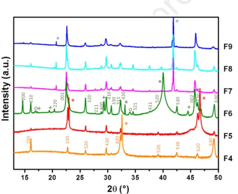
Samples were also grown with various target-substrate distances on C-plane sapphire
substrate, i.e. D = 65 mm (film F7), D = 60 mm (film F8), 55 mm (film F9) and 50 mm (not shown). For F7 and F8 films, similar XRD patterns and surface morphologies were observed (see Figure 5 and Figure 6 and related discussion hereafter). For F9 film however, a slight amount of the KNb3O8 phase is noticed on XRD pattern. Independently of the substrate type,
a target-substrate distance under 60 mm has resulted in the formation of secondary phases. In the following work this distance has been selected to be equal at least to 60 mm.
In order to control the orientation two films were deposited on SrTiO3 substrates, F4
on (110)SrTiO3 and F5 on (001)SrTiO3. In both cases, pure TTB coatings were obtained.
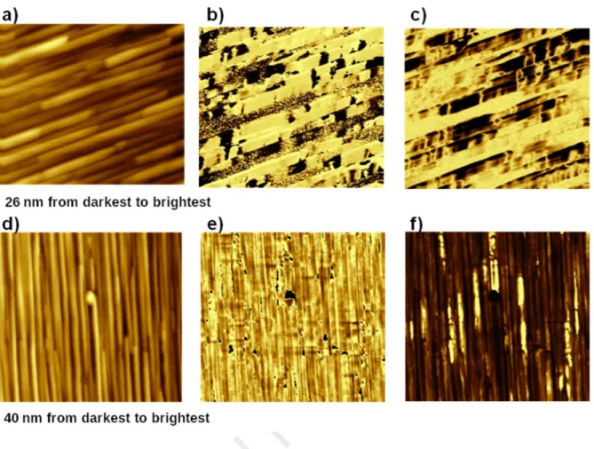
XRD pattern of the film F4 presents pure {hk0} TTB phase peaks with a strong (210) preferential orientation (Figure 5), in agreement with XRD and TEM observations performed on F3. Nonetheless, SEM micrograph F4 shows crystallites with parallelepiped-shape and shorter than for film F3 (about 50 nm wide and up to 700 nm long, Figure 6a). It could be noted that SEM images of the films synthetized from the T3 target do not exhibit any additional outgrowths or droplets that can often be observed, especially with targets of the KNN system phases which are difficult to densify by conventional synthesis.
Figure 5. XRD patterns of TTB films grown on (110)STO (film F4, D = 65 mm), (001)STO (film F5, D = 65 mm), (111)Pt/TiO2/SiO2/(001)Si (film F6, D = 60 mm) and C-plane sapphire (film F7, D = 65 mm), (film F8, D
= 60 mm), (film F9, D = 55 mm) (*: substrates; o: KNb3O8; + K3Nb7O19) (logarithmic scale).
Regardless of the SrTiO3 substrate orientation, nanorods present a quite perfect in-plane
orientation with almost no vertical nanorods growing along the c-axis parallel to the normal of the substrate. On (110) SrTiO3, the nanorods present a (210) out-of-plane main orientation
and are all growing parallel to each other along the same in-plane direction (film F4, Figure 6a), in line with a lowering of the mismatch between film and substrate cells along this direction (see discussion on the epitaxial relationships for F3). On the (001) SrTiO3 substrate
(film F5, figure 6b), the nanorods are growing along two in-plane directions with a 90° angle to each other (Figure 6b) with a (310) out-of-plane preferential orientation. Corresponding EDP registered along the [310] zone axis (Figure 7b) shows a pseudo-cubic array of reflections. The (001)SrTiO3 substrate involves this particular orientation due to the small
mismatch between the cubic (100) × (010) cell of SrTiO3 with d100× d010 = 3.905 Å × 3.905 Å
dimensions and the pseudo-cubic cell (001) × (130) of the TTB phase with d001× d310 = 3.99
Å × 3.937 Å dimensions. These experimental values were determined from the XRD (310) peak position and from the EDP (001) reflection of the individual nanorods registered in microdiffraction conditions (Figures 7d and 7f), respectively. Mismatches between the substrate and the film cells are respectively δ1 = [d(100)STO – d(001)TTB]/ d(100)STO = -2.17 %
and δ2 = [d(010)STO – d(130)TTB]/ d(010)STO = -0.84 %. Note that, in contrast to (110)SrTiO3
substrate, the square cell of the (001)SrTiO3 plane leads to equivalent mismatches at 90° from
each other, explaining the growth of the KNN TTB nanorods along two in-plane orientations as observed in Figure 6b. The corresponding lattice parameters were computed as a = 12.453 ± 0.005 Å (XRD) and c = 3.99 ± 0.05 Å (EDP).
Figure 6. Scanning electron micrographs of the TTB films grown on: (a) (110)STO (film F4, D = 65 mm); (b) (001)STO (film F5, D = 65 mm); (c) (111)Pt/TiO2/SiO2/(001)Si (film F6, D = 60 mm); (d) C-plane sapphire
(film F7, D = 65 mm); (e) C-plane sapphire (film F8, D = 60 mm), (f) C-plane sapphire (film F9, D = 55 mm).
In addition, microdiffraction pattern of the individual nanorods shows diffuse scattering lines along the [130] growth direction, indicating some planar disorder perpendicularly to this direction. By dark field method in 2-beams conditions, it was also possible to enlighten individual nanorods along the two different in-plane directions by selecting corresponding diffraction reflections (Figure 7c and 7e).
Figure 7. (a) Bright field TEM micrograph of the TTB films grown on (001)STO (film F5); (b) corresponding selected area EDP along the [310] zone axis; (c,e) Dark field TEM micrographs showing individual nanorods growing along the two in-plane directions; (d,f) Microdiffraction EDP of each nanorod variant along the [310] zone axis; (g,h) Bright field TEM micrograph and EDP along the [110] zone axis of the
TTB film grown on C-plane sapphire (film F7). The arrow displays the crystallite corresponding to the EDP.
Thin films were also deposited on Pt and sapphire substrates to perform dielectric
characterizations (at low frequency and at microwaves, respectively). XRD pattern of the thin film grown on (111)Pt/TiO2/SiO2/(001)Si (film F6) indicates a polycrystalline growth (i.e.
random orientation) with a (001) preferential orientation of the nanorods (Figure 5). In that case, the nanorods have grown as thin rod aggregates attached together by their longer edge, as observed on SEM micrograph (Figure 6c). The (001) preferential orientation is consistent with the presence of vertical agglomerated nanorods forming a flower-like microstructure. XRD pattern also exhibits minor secondary phases identified as KNb3O8 and K3Nb7O19
(JCPDS files # 01-075-2182 and #00-084-0812, respectively). The presence of secondary phases in films grown on Pt coated silicon, in contrast to those grown on SrTiO3, could be
explained by its higher thermal conductivity that increases the substrate surface temperature for the same deposition temperature. It is assumed that these phases presence has a minor impact on the thin film properties due to their small amount (Figure 5).
On C-plane sapphire, XRD patterns on F7 and F8 films show pure TTB phase (Figure 5). For both samples, those patterns exhibit a similar (001/310) preferential growth. TEM experiments performed on the F7 film confirm the elongation direction of nanorods along [001] direction (Figure 7g and 7h). EDXS analyses indicate a lower alkaline elements amount in the TTB nanorods compared with those grown on SrTiO3 (Table 2). However on both
substrates, the films present a sodium/potassium ratio close to 1 and an alkaline elements/niobium ratio slightly lower than the nominal composition (K,Na)0.6Nb1.1NbO3,
indicating that some cationic sites are therefore partially filled.
3.2. Investigation of the structural characteristics by Raman spectroscopy
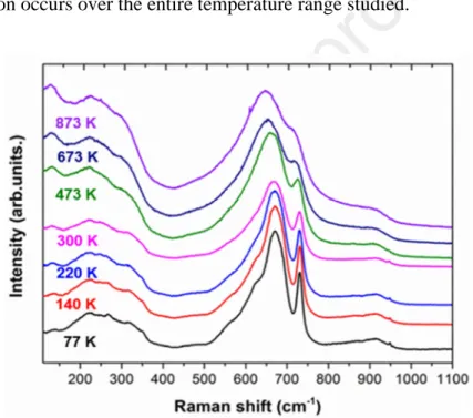
Figure 8 shows Raman spectra of the TTB thin film grown on (111)Pt/TiO2/SiO2/(001)Si
substrate (film F6). At room temperature, the spectra present typical signature of TTB phases compared with that reported for isostructural system [37–41], in agreement with X-ray diffraction and TEM analyses. Modes at 670 cm-1 and 731 cm-1 are assigned to the Nb–O stretching vibrations in the [NbO6] octahedra, and modes located in the 70 to 400 cm-1 range
is attributed to the O–Nb–O bending modes between adjacent [NbO6] octahedra, as observed
on other TTB niobates. The broad peaks with important contribution overlap, especially at low frequency region (< 400 cm-1), are characteristic of the TTB structure with cationic disorder in A1, A2 and C sites. These effects make the assignment of Raman lines hardly attainable, and so, it is impossible to distinguish unambiguously a centrosymmetrical structure from a non-centrosymmetrical one. Temperature-dependent spectra show neither significant shift nor anomaly in peak position and splitting or number modes change between 77 K and 873 K. This result strongly suggests a stable film structure and no clear evidence of any structural transition occurs over the entire temperature range studied.
Figure 8. Raman spectra of the TTB thin film deposited on (111)Pt/TiO2/SiO2/(001)Si (film F6) at various
temperatures (from 77 K to 873 K)
Figure 9. PFM of perovskite (F2) and TTB (F3) films: (a,d) topography; (b,e) phase; (c,f) amplitude. 2 µm × 2
µm size images
Piezoelectric Force Microscopy performed in topography mode on F2 and F3 films shows the typical morphologies of the perovskite and TTB-type KNN phases grown on (110)SrTiO3
(Figure 9a and 9d). In piezoresponse mode (Figure 9b, 9c, 9e and 9f), a clear contrast is observed in both cases, with a heterogeneous piezoelectric response: some grains show a strongest response (bright areas in Figure 9c and 9f) compared with others, with quasi-null amplitude response (dark areas in Figure 9c and 9f). In the case of the perovskite phase (Figure 9a-9c), where the PFM phase signal presents opposite directions of vertical polarization (the histogram of phase values (not shown) is composed of two peaks separated by 180°), this can be explained by a polarization direction in the orthorhombic cell with various directions relatively to the preferential orientation. Indeed the polarization in this kind of perovskite is aligned along the diagonal of the facets of the pseudo-cubic cell, i.e. the
<110> directions. In the present case, these directions correspond either to the normal direction or to the in-plane direction. Concerning the TTB phase, it is expected that the polarization direction is parallel to the [001] direction, therefore to the nanorod growth direction. Whereas a piezoresponse was observed, it has not been possible to reverse the signal by applying a reversed DC bias voltage. This experimental result is assigned to high leakage currents that make impossible to reach the coercive electric field without destroying the sample by Joule effect. In the case of the TTB phase whose properties are not fully established, another possibility concerns the piezoelectric response without ferroelectricity of the sample, at least at room temperature.
3.4. Dielectric characteristics 3.4.1. Low frequency measurements
The dielectric characteristics (εr and tanδ) at low frequencies were retrieved from the KNN
TTB thin film (F6) grown on (111)Pt/TiO2/SiO2/(001)Si substrate. No frequency dispersion of
the dielectric characteristics was observed from 1 kHz to 1 MHz with a permittivity value εr ≈
200 and tan
δ
≈ 1.5% (Figure 10). The recorded permittivity values are in the same range as to those of other TTB thin films, for instance εr ≈ 400 for K3Li2Nb5O15 epitaxial films [42] and ∼150 for Ba2LnFeNb4O15 (Ln = La, Nd, Eu) polycrystalline films [43], or to other values thatcan be found for ferroelectric thin films or dielectric relaxors as in the Bi-Zn-Nb-O system [44]. It has to be pointed out that polarization versus electric field measurements have been attempted. However, the high leakage currents make difficult the measurements under DC electric field and it was not possible to observe hysteretic loop with saturation of the polarization.
Figure 10. Variation of the dielectric characteristics (permittivity εrand loss tanδ) at low frequencies of the TTB
thin film (F6) deposited on (111)Pt/TiO2/SiO2/(001)Si.
3.4.2. High frequency measurements
The dielectric characteristics (εr and tanδ) at high frequencies were retrieved from the KNN
TTB thin film (F8) grown on C-plane sapphire substrate. The values were obtained using the measured reflection (S11) and transmission (S21) coefficients of the transmission lines. TTB
thin film exhibits a permittivity εr = 135 at 10 GHz, 130 at 20 GHz, and 125 at 30 GHz
showing a good stability versus frequency (Figure 11a). Even though the literature does not present many microwave dielectric characterizations of the TTB phases, permittivity values close to 130 have also been reported for other materials [45, 46]. Nevertheless, these values remain lower than those retrieved from the KxNa1-xNbO3 perovskite phase in the same settings
[47]. The dielectric permittivity decrease of the TTB phase from εr ≈ 200 at low frequency to
εr ≈ 130 at high frequency is consistent with the decrease as reported in the literature. The loss tangent value tanδ at 10 GHz is about 20 % (Figure 11). The variation of tanδ from 1 to 5 GHz is attributed in part of the metal skin depth loss. tanδ at high frequencies remains much higher than 1.5 % measured at low frequency. The polyoriented growth of the TTB phase,
especially both in-plane and out-of-plane ordering of the nanorods, led to a quite rough film, and consequently to a rough metal-oxide film interface which may impact the loss.
The dielectric characteristics (εr and tanδ) at 10 GHz have shown no significant temperature
dependence from 20°C to 240°C (Figure 11b). The variation of the permittivity and the slight increase in tanδ from 20% to 23% are attributed to the temperature increase of the device as a whole and of the measurement system. Therefore, the variations are not significant enough to hint a phase transition and are in agreement with the previous observations by Raman spectroscopy. The results also indicate a good stability of the dielectric characteristics at microwave frequencies in this range of temperature.
Figure 11. Variation of the dielectric characteristics (permittivity εr and loss tanδ) at high frequencies of the
TTB thin film (F8) deposited on C-cut sapphire (a) depending on the frequency at room temperature and (b) depending on the temperature at 10 GHz.
The dielectric characteristics were also retrieved from the transmission lines under biasing (Ebias up to 27 kV/cm). No significant change was observed. Moreover the resonance
frequency Fr of the CPW stub resonator printed on the KNN thin film was measured under
various biasing to investigate a possible tunability (not shown here). A slightly open cycle shape has been evidenced, which could suggest a ferroelectric-like behavior. However the weak variation leading to a frequency tunability value lower than 1% could not be considered as a proof of a ferroelectric behavior.
CONCLUSION
A tetragonal tungsten bronze structure in the K-Na-Nb-O system was successfully synthesized in thin films on various substrates using pulsed laser deposition technique. Thin films were deposited on both (100) and (110)SrTiO3 with a highly oriented growth. Indeed dense
microstructures with characteristic in-plane oriented nanorods were evidenced. Complementary characterizations (i.e. X-ray and electron diffraction, Raman spectroscopy) have also evidenced the TTB type phase growth. Piezoelectric Force Microscopy has shown an unambiguous piezoelectric local activity. However, high leakage currents made them impossible to switch the TTB polarization under an external DC electric field without destroying the sample.
Dielectric characteristics at room temperature were retrieved at low and high frequencies with a dielectric permittivity εr ≈ 200 at 1 kHz and 130 at 10 GHz from thin films
electrical measurements, that were also restricted by high leakage current, have not shown ferroelectricity.
In order to perform further investigations on the physical behavior, it is essential to suppress the leakage current. For this purpose and to decrease loss, chemical doping could be envisaged as it has been performed in KxNa1-xNbO3 perovskite phase [48]. Indeed, the vacant
crystallographic sites which characterize the TTB structure give a large possibility of improvement, modification and control of the TTB properties.
AKNOWLEDGEMENTS
The authors warmly thank Dr. S. Quémeré and Dr. P. Lemoine for their help in SPS experiments, C. Derouet for technical assistance for X-Ray diffraction, and S. Ollivier for her assistance in thin films preparation and characterization (ISCR) and P. Hamoumou for his assistance for PFM measurements (INL).
The scanning electron microscopy and transmission electron microscopy were performed in ScanMAT UMS 20001 CNRS-University of Rennes 1.
The authors are grateful for the financial support of the Direction Générale de l’Armement (DGA) and the Région Bretagne (PhD research Grant of B. Aspe, project ARMin). ISCR and ScanMAT received a financial support from the Région Bretagne, Rennes Métropole, the Département d’Ille et Vilaine and the European Union (CPER-FEDER 2007–2014, Présage Nos. 39126 and 37339, and CPER SCANMAT 2015-2020 MULTIMAT ScanMAT). This work was also supported by the European Union through the European Regional Development Fund (ERDF), the Ministry of Higher Education and Research, the Région Bretagne, the Département des Côtes d’Armor and Saint-Brieuc Armor Agglomération,
through the CPER Projects 2015-2020 MULTIMAT MATECOM and SOPHIE / STIC & Ondes.
REFERENCES
1. D.L. Polla, Microelectromechanical systems based on ferroelectric thin films.
Microelectron Eng 29:51–58 (1995). https://doi.org/10.1016/0167-9317(95)00114-X 2. N. Setter,D. Damjanovic, L. Eng, G. Fox, S. Gevorgian, S. Hong, A. Kingon, H.
Kohlstedt, N.Y. Park, G.B. Stephenson, I. Stolitchnov, A.K. Taganstev, D.V. Taylor, T. Yamada, S. Steiffer, Ferroelectric thin films: Review of materials, properties, and applications. J Appl Phys 100:051606 (2006). https://doi.org/10.1063/1.2336999 3. A. Petosa, An Overview of Tuning Techniques for Frequency-Agile Antennas. IEEE
Antennas Propag Mag 54:271–296 (2012). https://doi.org/10.1109/MAP.2012.6348178 4. V. Ishchuk, D. Kuzenko, V. Sobolev, Piezoelectric and functional properties of materials
with coexisting ferroelectric and antiferroelectric phases. AIMS Mater Sci 5:711–741 (2018). https://doi.org/10.3934/matersci.2018.4.711
5. Y. Saito, H. Takao, T. Tani, T. Nonoyama, K. Takatori, T. Homma, T. Nagaya, M. Nakamura, Lead-free piezoceramics. Nature 432:84–87 (2004).
https://doi.org/10.1038/nature03028
6. J.-F. Li, K. Wang, F.-Y. Zhu, L.-Q. Cheng, F.-Z. Yao, (K,Na)NbO3-Based Lead-Free
Piezoceramics: Fundamental Aspects, Processing Technologies, and Remaining
Challenges. J Am Ceram Soc 96:3677–3696 (2013). https://doi.org/10.1111/jace.12715 7. J. Wu, D. Xiao, J. Zhu, Potassium–Sodium Niobate Lead-Free Piezoelectric Materials:
Past, Present, and Future of Phase Boundaries. Chem Rev 115:2559–2595 (2015). https://doi.org/10.1021/cr5006809
8. M.R. Bafandeh, R. Gharahkhani, J.-S. Lee, Dielectric and piezoelectric properties of sodium potassium niobate-based ceramics sintered in microwave furnace. Mater Chem Phys 156:254–260 (2015). https://doi.org/10.1016/j.matchemphys.2015.03.018
9. M. Peddigari, V. Patel, G.P. Bharti, A. Khare, D. Pamu, Microwave dielectric and nonlinear optical studies on radio-frequency sputtered Dy2O3-doped KNN thin films. J
Am Ceram Soc 100:3013–3023 (2017). https://doi.org/10.1111/jace.14846
10. F. Fan, X. Zhao, F. Wang, Q. Yue, H. Zhou, H. Luo, Y. Tang, Z. Duan, W. Shi, B. Fang, Design and fabrication of high frequency ultrasonic transducer based on lead-free Mn-doped (K0.44Na0.56)NbO3 single crystal. Sens Actuators Phys 267:182–186 (2017).
https://doi.org/10.1016/j.sna.2017.10.018
11. Y. Sun, F. Guo, Q. Lu, S. Zhao, Improved ferroelectric photovoltaic effect in Mn-doped lead-free K0.5Na0.5NbO3 films. Ceram Int 44:13994-13998 (2018).
12. J.-C. Grivel, K. Thydén, J.R. Bowen, A.B. Haugen, Deposition of highly oriented (K,Na)NbO3 films on flexible metal substrates. Thin Solid Films 650:7–10 (2018).
https://doi.org/10.1016/j.tsf.2018.02.008
13. J. Du, Z. Xu, R. Chu, J. Hao, W. Li, G. Jiang, P. Zheng, Rare-earth doped
(K0.5Na0.5)NbO3 multifunctional ceramics. J Mater Sci Mater Electron 28:5288–5294
(2017). https://doi.org/10.1007/s10854-016-6186-6
14. R. Castañeda-Guzmán, R. López-Juárez, J.J. Gervacio, M.P. Cruz, S. Díaz de la Torre, S.J. Pérez-Ruiz, Structural and piezo-ferroelectric properties of K0.5Na0.5NbO3 thin films
grown by pulsed laser deposition and tested as sensors. Thin Solid Films 636:458–463 (2017). https://doi.org/10.1016/j.tsf.2017.06.039
15. S. Garroni, N. Senes, A. Iacomini, S. Enzo, G. Mulas, L. Pardo, S. Cuesta-Lopez, Advanced Synthesis on Lead-Free KxNa(1−x)NbO3 Piezoceramics for Medical Imaging
Applications. Phys Status Solidi A 1700896 (2018). https://doi.org/10.1002/pssa.201700896
16. Q. Simon, V. Dorcet, P. Boullay, V. Demange, S. Députier, V. Bouquet, M. Guilloux-Viry, Nanorods of Potassium Tantalum Niobate Tetragonal Tungsten Bronze Phase Grown by Pulsed Laser Deposition. Chem Mater 25:2793–2802 (2013).
https://doi.org/10.1021/cm401018k
17. B.A. Scott, E.A. Giess, B.L. Olson, G. Burns, A.W. Smith, D.F. O'Kane, The tungsten bronze field in the system K2O|Li2O|Nb2O5. Mater Res Bull 5:47–56 (1970).
https://doi.org/10.1016/0025-5408(70)90072-3
18. A.A. Awadalla, B.M. Gatehouse, Crystal structures of some niobium and tantalum oxides. III K6Ta10.8O30 - A partially “Filled” tetragonal tungsten bronze-like structure. J
Solid State Chem 23:349–355 (1978). https://doi.org/10.1016/0022-4596(78)90083-X 19. M. Lundberg, M. Sundberg, Studies of phases in the KNbO3-Nb2O5 system by
high-resolution electron microscopy and X-ray powder diffraction. J Solid State Chem 63:216–230 (1986). https://doi.org/10.1016/0022-4596(86)90172-6
20. F. Madaro, R. Sæterli, J.R. Tolchard, M.-A. Einarsrud, R. Holmestad, T. Grande, Molten salt synthesis of K4Nb6O17, K2Nb4O11 and KNb3O8 crystals with needle- or plate-like
morphology. CrystEngComm 13:1304–1313 (2011). https://doi.org/10.1039/C0CE00413H
21. A. Simon, J. Ravez, Solid-state chemistry and non-linear properties of tetragonal tungsten bronzes materials. Comptes Rendus Chim 9:1268–1276 (2006).
https://doi.org/10.1016/j.crci.2006.04.001
22. R.R. Neurgaonkar, W.K. Cory, J.R. Oliver, L.E. Cross, Growth and properties of tungsten bronze K3Li2Nb5O15 single crystals. Mater Res Bull 24:1025–1030 (1989).
https://doi.org/10.1016/0025-5408(89)90188-8
23. X. Fan, Y. Wang, Y. Jiang, Structure and electrical properties of MnO2-doped
Sr2−xCaxNaNb5O15 lead-free piezoelectric ceramics. J Alloys Compd 509:6652–6658
24. R.Q. Yin, P. Zheng, J.C. Wang, L.M. Dai, J. Du, L. Zheng, J.X. Deng, K.X. Song, H.B. Qin, Structural and electrical properties of K-doped Sr1.85Ca0.15NaNb5O15 lead-free
piezoelectric ceramics. Ceram Int 42:10349–10354 (2016). https://doi.org/10.1016/j.ceramint.2016.03.159
25. R.Z. Mehdiyeva, A.I. Mammadov, R.E. Huseynov, S. Kafarova, T. Çoşkun, M.Y. Seyidov, Preparation, structure analysis and dielectric characteristics of the novel ferroelectric ceramics (1−x)Sr3.35Ba1.65Nb10O30(SBN)-(x)Ba4Na2Nb10O30 (BNN) with
potassium tungsten-bronze structure. J Alloys Compd 711:169–183 (2017). https://doi.org/10.1016/j.jallcom.2017.03.309
26. G. Zhu, Z. Ci, C. Ma, Y. Shi, Y. Wang, A novel red emitting phosphor of Eu3+ doped TTB-type niobate NaSr2Nb5O15 for white LEDs. Mater Res Bull 48:1995–1998 (2013).
https://doi.org/10.1016/j.materresbull.2012.12.074
27. A. Kudo, H. Okutomi, H. Kato, Photocatalytic Water Splitting into H2 and O2 over
K2LnTa5O15 Powder. Chem Lett 29:1212–1213 (2000).
https://doi.org/10.1246/cl.2000.1212
28. J. Hreščak, B. Malič, J. Cilenšek, A. Benčan, Solid-state synthesis of undoped and Sr-doped K0.5Na0.5NbO3: Study by thermal analysis and in situ high-temperature X-ray
diffraction. J Therm Anal Calorim 127:129–136 (2017). https://doi.org/10.1007/s10973-016-5615-3
29. F. Rubio-Marcos, P. Marchet, T. Merle-Méjean, J.F. Fernandez, Role of sintering time, crystalline phases and symmetry in the piezoelectric properties of lead-free KNN-modified ceramics. Mater Chem Phys 123:91–97 (2010).
https://doi.org/10.1016/j.matchemphys.2010.03.065
30. J. Fuentes, J. Portelles, M.D. Durruthy-Rodríguez, H. H'Mok, O. Raymond, J. Heiras, M.P. Cruz, J.M. Siqueiros, Dielectric and piezoelectric properties of the KNN ceramic compound doped with Li, La and Ta. Appl Phys A 118:709–715 (2015).
https://doi.org/10.1007/s00339-014-8783-7
31. A. Waroquet, V. Demange, N. Hakmeh, J. Perrière, S. Freslon, S. Députier, M. Guilloux-Viry, Epitaxial growth and cationic exchange properties of layered KNb3O8
thin films. RSC Adv 7:15482–15491 (2017). https://doi.org/10.1039/C7RA00261K 32. A. Waroquet, Couches-minces dans le système K-Nb-O : croissance épitaxiale et
nanostructuration par PLD de phases pérovskite, TTB et lamellaires. Thesis, Rennes 1, (2015).
33. S. Mustofa, T. Araki, T. Furusawa, M. Nishida, T. Hino, The PLD of BaTiO3 target
produced by SPS and its electrical properties for MLCC application. Mater Sci Eng B 103:128–134 (2003). https://doi.org/10.1016/S0921-5107(03)00160-0
34. M. Bah, F. Giovannelli, F. Schoenstein, G. Feuillard, E. Le Clezio, I. Monot-Laffez, High electromechanical performance with spark plasma sintering of undoped
K0.5Na0.5NbO3 ceramics. Ceram Int 40:7473–7480 (2014).
35. Q. Simon, Y. Corredores, X. Castel, R. Benzerga, R. Sauleau, K. Mahdjoubi, A. Le Febvrier, S. Députier, M. Guilloux-Viry, L. Zhang, P. Laurent, G. Tanné, Highly tunable microwave stub resonator on ferroelectric KTa0.5Nb0.5O3 thin film. Appl Phys Lett
99:092904 (2011). https://doi.org/10.1063/1.3626040
36. F. Brik, R. Enjalbert, C. Roucau, J. Galy, TTB Structure of K4Ce2M10O30(M= Nb or Ta):
Crystal Growth and Joint X-Ray and HREM Studies. J Solid State Chem 122:7–14 (1996). https://doi.org/10.1006/jssc.1996.0073
37. G. Burns, J.D. Axe, D.F. O’Kane, Raman measurements of NaBa2Nb5O15 and related
ferroelectrics. Solid State Commun 7:933–936 (1969). https://doi.org/10.1016/0038-1098(69)90545-6
38. V. Hornebecq, C. Elissalde, V. Porokhonskyy, V. Bovtun, J. Petzelt, M. Maglione, J. Ravez, Dielectric relaxation in tetragonal tungsten bronze ceramics. J Phys Chem Solids 64:471–476 (2003). https://doi.org/10.1016/S0022-3697(02)00342-6
39. Y. Amira, Y. Gagou, A. Menny, D. Mezzane, A. Zegzouti, M. Elaatmani, M. El Marssi, Structural and Raman properties of the tetragonal tungsten bronze ferroelectric
Pb2(1−x)K1+xGdxNb5O15. Solid State Commun 150:419–423 (2010).
https://doi.org/10.1016/j.ssc.2009.12.004
40. A.R.F. Lima, J.C. Sczancoski, M. Siu Li, E. Longo, E.R. Camargo, Structural
characterization and photoluminescence behavior of pure and doped potassium strontium niobates ceramics with tetragonal tungsten–bronze structure. Ceram Int 42:4709–4714 (2016). https://doi.org/10.1016/j.ceramint.2015.11.130
41. Y. Yao, K. Guo, D. Bi, T. Tao, B. Liang, C.L. Mak, S.G. Lu, Pyroelectric properties of calcium doped strontium barium niobate ceramics Sr0.65−xCaxBa0.35Nb2O6 (x = 0.05–
0.425). J Mater Sci Mater Electron 29:17777–17785 (2018). https://doi.org/10.1007/s10854-018-9885-3
42. B. Allouche, Y. Gagou, A. Belboukhari, F. Le Marrec, M. El Marssi, Structural and electrical properties of K3Li2Nb5O15 thin film grown by pulsed laser deposition. Mater
Res Bull 94:287–290 (2017). https://doi.org/10.1016/j.materresbull.2017.06.018 43. R. Bodeux, D. Michau, M. Josse, M. Maglione, Dielectric properties of tetragonal
tungsten bronze films deposited by RF magnetron sputtering. Solid State Sci 38:112–118 (2014). https://doi.org/10.1016/j.solidstatesciences.2014.10.007
44. A. Le Febvrier, S. Députier, V. Demange, V. Bouquet, A.C. Galca, A. Iuga, L. Pintilie, M. Guilloux-Viry, Effect of in-plane ordering on dielectric properties of highly {111}-oriented bismuth–zinc–niobate thin films. J Mater Sci 52:11306–11313 (2017). https://doi.org/10.1007/s10853-017-1297-x
45. Z. Xiong, B. Tang, C. Yang, S. Zhang, Correlation between structures and microwave dielectric properties of Ba3.75Nd9.5-xSmxTi17.5(Cr1/2Nb1/2)0.5O54 ceramics. J Alloys Compd
740:492–499 (2018). https://doi.org/10.1016/j.jallcom.2017.10.072
46. K. Fukuda, R. Kitoh, I. Awai, Microwave characteristics of BaPr2Ti4O12 and
BaPr2Ti5O14 ceramics. J Mater Res 10:312–319 (1995).
47. B. Aspe, F. Cissé, X. Castel, V. Demange, S. Députier, S. Ollivier, V. Bouquet, L. Joanny, R. Sauleau, M. Guilloux-Viry, KxNa1−xNbO3 perovskite thin films grown by
pulsed laser deposition on R-plane sapphire for tunable microwave devices. J Mater Sci 53:13042–13052 (2018). https://doi.org/10.1007/s10853-018-2593-9
48. S.Y. Lee, C.W. Ahn, A. Ullah, H.J. Seog, J.S. Kim, S.H. Bae, I.W. Kim, Effect of Mn substitution on ferroelectric and leakage current characteristics of lead-free
(K0.5Na0.5)(MnxNb1−x)O3 thin films. Curr Appl Phys 11:S266–S269 (2011).
Highlights:
• Pure tetragonal tungsten bronze phase films were grown by PLD in the KNN system
• The TTB structural features were shown by transmission electron microscopy and XRD
• Highly oriented thin films were grown on (100) and (110) SrTiO3 substrates • Dielectric characteristics were determined at low frequencies and in microwave
Declaration of interests
☒The authors declare that they have no known competing financial interests or personal relationships that could have appeared to influence the work reported in this paper.
☐The authors declare the following financial interests/personal relationships which may be considered as potential competing interests:
![Figure 1. Projection of the tetragonal tungsten bronze structure along the [001] direction showing the three cationic tunnels A1, A2, and C, and the cationic octahedral sites B1 and B2 [16].](https://thumb-eu.123doks.com/thumbv2/123doknet/8128451.272824/5.892.306.639.113.458/projection-tetragonal-tungsten-structure-direction-cationic-cationic-octahedral.webp)