HAL Id: hal-00380072
https://hal.archives-ouvertes.fr/hal-00380072
Submitted on 27 Apr 2020
HAL is a multi-disciplinary open access
archive for the deposit and dissemination of
sci-entific research documents, whether they are
pub-lished or not. The documents may come from
teaching and research institutions in France or
abroad, or from public or private research centers.
L’archive ouverte pluridisciplinaire HAL, est
destinée au dépôt et à la diffusion de documents
scientifiques de niveau recherche, publiés ou non,
émanant des établissements d’enseignement et de
recherche français ou étrangers, des laboratoires
publics ou privés.
Investigation of point defect generation in dry etched
InP ridge waveguide structures
M. Avella, J. Jimenez, F. Pommereau, J.P. Landesman, A. Rhallabi
To cite this version:
M. Avella, J. Jimenez, F. Pommereau, J.P. Landesman, A. Rhallabi. Investigation of point defect
generation in dry etched InP ridge waveguide structures. Applied Physics Letters, American Institute
of Physics, 2007, 90 (22), pp.223510. �10.1063/1.2743384�. �hal-00380072�
Investigation of point defect generation in dry etched InP ridge
waveguide structures
M. Avella and J. Jiméneza兲
Física Materia Condensada, ETSII, 47011 Valladolid, Spain
F. Pommereau
Alcatel-Thales III-V Laboratory, 91128 Palaiseau, France
J. P. Landesman and A. Rhallabi
Laboratoire des Plasmas et des Couches Minces, Institut des Matériaux, UMR6502 CNRS, 2, Rue de la Houssinière, 44322 Nantes cedex 3, France
共Received 26 November 2006; accepted 3 May 2007; published online 1 June 2007兲
Waveguides engraved in InP by dry etching, reactive ion etching and inductively coupled plasma 共ICP兲, were studied by cathodoluminescence. The dry etching processes were found to induce nonradiative recombination centers, which reduce the luminescence emission from the ridge structures. In addition, the ICP process introduced intrinsic defects, probably In vacancy related defects, which were generated at the dielectric cap/InP interface at the ridge top. © 2007 American
Institute of Physics. 关DOI:10.1063/1.2743384兴
Ion etching techniques are used for the fabrication of III-V semiconductor structures with submicrometric lateral dimension.1Therefore, they are basic tools for the fabrication of optoelectronic devices, such as vertical cavity surface emitting lasers, buried heterostructure lasers, and photonic crystals for integrated optical devices.2 In this type of de-vices, one aims for vertical sidewalls and smooth surfaces, because rough etched surfaces lead to enhanced surface re-combination velocity 共SRV兲, light scattering, and optical propagation losses that affect the device performance and reliability. Therefore, most of the work concerning the char-acterization of selective area etched structures is based on the morphology analysis, e.g., the aspect ratio and the verticality of the etched sidewalls, and the surface damage.3,4In the last few years, inductively coupled plasma 共ICP兲 has had more applications, since it allows low ion energy 共⬍100 eV兲 with higher etching rate than reactive ion etching 共RIE兲 does while maintaining smooth surfaces.
One of the collateral effects of the ion etching is the formation of defects. The study of these effects has mainly concerned the etched surfaces, with special emphasis paid to the etched sidewalls. However, as important as the etched surfaces are the micrometric engraved structures, which con-stitute the active parts of the devices and have not received enough attention. The generation of point defects in these structures has been normally indirectly measured by studying quantum well intermixing enhanced by the diffusion of point defects under thermal annealing.5,6 However, a complete view of where the defects are formed during the etching step is still lacking. The study of small structures should require the use of spectroscopic techniques with submicrometric spa-tial resolution. In particular, cathodoluminescence 共CL兲 in the scanning electron microscope 共SEM兲 appears as a unique tool to study such structures because of its high spatial reso-lution, its coupling to the morphology observation in the SEM, and its spectroscopic capabilities.
The CL measurements were carried out at 80 K in a XiCLOne system from Gatan. The detection is carried out by means of a charge coupled device camera allowing the ac-quisition of the full spectrum for each e-beam scanned pixel. Etched structures were studied in both top view and cross section on cleaved surfaces.
The samples were fabricated on bulk 共100兲 InP S doped at 1.5⫻ 1018cm−3. A 400 nm silicon nitride layer was depos-ited by plasma enhanced chemical vapor deposition at 250 ° C. Ridge patterns with various widths ranging from 1 to 3m were defined in a positive photoresist by contact lithography and transferred into SiNx by RIE using a
SF6/ CHF3/ O2 gas mixture. After resist and polymer
strip-ping in an O2microwave plasma asher, the ridge stripes have
been transferred into InP by RIE or ICP etching.
The RIE was carried out on an Adixen GIR100 equip-ment using a mixture of CH4/ H2gases. The ion energy at the
surface of the sample was as high as 470 V. This was the value of the voltage at the cathode. The beam current density was estimated at 3 mA/ cm2. Hydrocarbon polymers which
formed along the sidewall of the ridges and on the SiN mask have been removed by O2microwave plasma etching.
The ICP etching was performed in an Adixen 601E equipment using SiCl4 based chemistry. The plasma is
ex-cited with a 13.56 MHz radio frequency 共rf兲 generator and
a兲
Electronic mail: jimenez@fmc.uva.es
FIG. 1. Panchromatic CL images of RIE 共left兲 and ICP 共right兲 ridges in top view.
APPLIED PHYSICS LETTERS 90, 223510 共2007兲
the sample is biased with a separate rf generator at 13.56 MHz. The resulting ion energy was optimized at 60 V and the ion beam current was estimated at 8 mA/ cm2. For both RIE and ICP treated samples the Si3N4 mask was
re-moved with fluorhydric acid. The ridge heights are 3.6 and 4m for RIE and ICP samples, respectively. For more de-tails about the experimental procedure, see Ref.7.
The CL images show a strong contrast between the ridge 共nonetched兲 and the etched floor for both ICP and RIE pro-cesses 共Fig.1兲. Surprisingly, the ridge displays a lower lumi-nescence intensity giving a dark contrast in the CL image, while the etched floor appears bright, contrary to the ex-pected behavior not only because the SRV of the etched re-gions must be enhanced due to surface damage but also be-cause the ion bombardment is expected to create point defects.3The low luminescence emission in the ridges can be due to the influence of the etched sidewalls, and/or the gen-eration of nonradiative recombination centers.
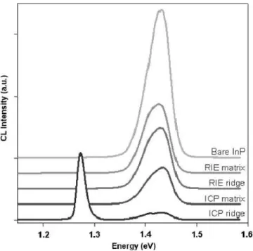
Local spectra were acquired in order to check the differ-ences between the two processes and the two regions, etched floor and nonetched ridges. The spectrum in the etched floor presents a broad near band gap 共NBG兲 band composed of at least two bands, corresponding to the band to band recombi-nation 共1.43 eV兲 and a shoulder peaking after deconvolution at 1.395 eV, which is usually associated with a free to bound transition. This is a typical spectrum of S-doped InP in the mid-1018-cm−3doping level. The peak energies are shifted to the blue due to conduction band filling 共Burstein-Moss
effect兲.8 This spectrum is common to both processes and is similar to the reference substrate 共Fig.2兲. What is different between the two etching processes is the spectrum inside the ridge. While the spectrum corresponding to the RIE process is similar to that observed in the etched region with the cor-responding intensity decrease, the spectrum in the ridge of the sample etched by ICP presents an additional band, peak-ing around 1.27 eV, the intensity of which can be as high as the one of the NBG band. This band evidences the genera-tion of bulk point defects during the ICP process in the re-gions that are not directly exposed to the ICP ion bombard-ment. The influence of a dielectric cap layer in the formation and diffusion of defects has been discussed in the case of InP and related alloys;9,10 however, temperatures much higher than the nominal temperature of the process 共the samples were thermalized at 20 ° C兲 are necessary to generate defects at the InP / SiNxinterface by the only thermal energy transfer.
Because the etched regions do not show additional lumines-cence bands related to defects, one can argue that the ICP process itself does not create the point defects in regions that are not capped with the dielectric layer. Therefore, the 1.27 eV band must arise from defects created during the ICP etching of micrometer structures by the presence of the di-electric capping layer. This luminescence band in InP is usu-ally associated with In vacancies or their complexes.11.
Ridges of different dimensions, 1 and 2m wide, re-spectively, were studied in cross section. The distribution of defects and the influence of the surface are seen in Fig. 3, where monochromatic images obtained at 1.43 eV 共866 nm兲 and 1.27 eV 共975 nm兲 for the ICP and RIE samples are shown. The images obtained at 1.43 eV show the recombi-nation pattern associated with the increase of the SRV by the etching processes at both the sidewalls and the etched floor and the nonradiative recombination activity of the InP / SiNx
interface on top of the ridge, where the luminescence inten-sity is drastically reduced. The luminescence inside the ridges is significantly reduced in the 1m wide ridge with respect to the 2m wide ridge, which is accounted for by the nonradiative recombination at the etched sidewalls, which have more relevance in narrow ridges 关see Fig.3共d兲兴. The 1.27 eV band in ICP etched structures is very intense on top of the ridge 关Figs.3共c兲and3共e兲兴; the highest intensity of the 1.27 eV band is found beneath the dielectric capping layer around 1m away from the interface; the nonradiative recombination centers are dominant in the region close to the interface. The distribution of this luminescence band shows that the point defects are generated at the InP / SiNxinterface
and thereafter they in-diffuse through the ridge expanding beneath the ridge when they reach the ridge base 关see Figs.
3共c兲and 3共e兲兴, where the amplitude of the 1.27 eV band is mapped in the two ICP etched ridges, 2 and 1m wide,
FIG. 2. CL spectra in different samples and positions 共see insert legend兲.
ICP ridge 2m wide 共1.27 eV兲, 共d兲 ICP ridge 1m wide 共1.43 eV兲, and 共e兲 ICP ridge 1m wide 共1.27 eV兲.
respectively. This distribution pattern evidences that the de-fects responsible for the 1.27 eV band are not generated at the sidewalls, nor at the etched floor. Therefore they are not a direct product of the ion bombardment. During ion bom-bardment the energy transfer from the incident ions, which lose the energy in cascade collisions, to the InP lattice can lower the potential barrier for defect formation and motion or can transfer heat to the lattice enhancing the temperature. The energy of the ions is higher in RIE than in ICP; however, the etching rate is 25 times faster in ICP with respect to RIE 共500 against 20 nm/ min兲, which suggests that the high ion flow and the nature of the etching gases are prevalent in the formation of the In vacancy related defects responsible for the 1.27 eV luminescence band. In this process, there is a higher transfer of energy to the lattice allowing the formation of the vacancy defects in the ICP process. It should be noted that the formation of those defects must be strongly depen-dent on the characteristics of the dielectric capping layer. The dielectric capping layer plays the role of a defect source dur-ing the ICP process. Therefore, the nature and stoichiometry of the dielectric are relevant to the formation of defects.12
On the other hand, the diffusionlike distribution of the 1.27 eV band 关Figs. 3共c兲 and 3共e兲兴, suggests that the tem-perature inside the ridge structures is enhanced during the etching process. The heat dissipation must be slowed due to the reduced dimension of the ridge structures; see that the narrow ridge 关Fig.3共e兲兴 shows a longer diffusion range than the wider ridge 关Fig.3共c兲兴. Further annealing experiments are necessary to elucidate the temperature enhancement inside the ridge structures during dry etching.
In summary, we have demonstrated that point defects are generated during the fabrication of ridgelike structures in InP
by ICP dry etching processes, but not by the RIE process. Indium vacancy related defects were observed in ICP etch-ing, which are responsible for an additional luminescence band at 1.27 eV. The generation of these point defects is located at the InP / SiNx interface and were demonstrated to
in-diffuse toward the base of the ridge during the etching process.
This work was carried out in the frame of the Spanish-French Cooperation Program 共Picasso Integrated Actions兲.
1
S. J. Choi, K. Djorjev, S. J. Choi, and P. D. Dapkus, J. Vac. Sci. Technol. B 20, 301 共2002兲.
2
Ch. Kim, W. J. Kim, A. Stapleton, J. R. Cao, J. D. O’Brien, and P. D. Dapkus, J. Opt. Soc. Am. B 19, 1777 共2002兲.
3
H. Iber, S. Mo, E. Peiner, G. Vollrath, A. Schlachetzki, and F. Fiedler, Semicond. Sci. Technol. 12, 755 共1997兲.
4
S. J. Pearton, F. Ren, W. S. Hobson, C. A. Green, and U. K. Chakrabarti, Semicond. Sci. Technol. 7, 1217 共1992兲.
5
B. S. Ooi, A. C. Bryce, C. D. W. Wilkinson, and J. H. Marsh, Appl. Phys. Lett. 64, 598 共1994兲.
6
Ching-Hui Chen, D. Ginger Yu, E. L. Hu, and P. M. Petroff, J. Vac. Sci. Technol. B 14, 3684 共1996兲.
7
F. Pommereau, L. Legouezigou, S. Hubert, S. Sainson, J. P. Chandouineau, S. Fabre, G. H. Duan, B. Lombardet, R. Ferrini, and R. Houdré, J. Appl. Phys. 95, 2242 共2004兲.
8
M. Bugaajski and W. Lewandowski, J. Appl. Phys. 57, 521 共1985兲. 9
S. Sudo, H. Onishi, Y. Nakano, Y. Shimogaki, K. Tada, M. J. Mondry, and L. A. Coldren, Jpn. J. Appl. Phys., Part 1 35, 1276 共1996兲.
10
W. J. Choi, H. T. Yi, J. I. Lee, and D. H. Woo, J. Korean Phys. Soc. 45, 773 共2004兲.
11
H. Temkin, B. V. Dutt, W. A. Bonner, and V. G. Keramidas, J. Appl. Phys.
53, 7526 共1982兲. 12
J. S. Yu, J. D. Song, Y. T. Lee, and H. Lim, J. Appl. Phys. 92, 1386 共2002兲.