HAL Id: hal-01343329
https://hal.archives-ouvertes.fr/hal-01343329
Submitted on 1 Apr 2019HAL is a multi-disciplinary open access archive for the deposit and dissemination of sci-entific research documents, whether they are pub-lished or not. The documents may come from teaching and research institutions in France or abroad, or from public or private research centers.
L’archive ouverte pluridisciplinaire HAL, est destinée au dépôt et à la diffusion de documents scientifiques de niveau recherche, publiés ou non, émanant des établissements d’enseignement et de recherche français ou étrangers, des laboratoires publics ou privés.
Low Frequency and linear high frequency noise
performances of AlGaN/GaN grown on SiC substrate
Jean-Guy Tartarin, Geoffroy Soubercaze-Pun, Laurent Bary, C. Chambon, S.
Gribaldo, Olivier Llopis, Laurent Escotte, Robert Plana, S Delage, Jacques
Graffeuil, et al.
To cite this version:
Jean-Guy Tartarin, Geoffroy Soubercaze-Pun, Laurent Bary, C. Chambon, S. Gribaldo, et al.. Low Frequency and linear high frequency noise performances of AlGaN/GaN grown on SiC substrate. IEEE 13th Gallium Arsenide and other compound semiconductors Application Symposium 2005, Oct 2005, Paris, France. pp.299-302, �10.1063/1.2036754�. �hal-01343329�
Low Frequency and linear high frequency noise
performances of AlGaN/GaN grown on SiC substrate
J.-G. Tartarin
1, G. Soubercaze-Pun
1, L. Bary
2, C. Chambon
1, S. Gribaldo
1, O. Llopis
2, L. Escotte
1,
R. Plana
1, S. Delage
3, C. Gaquière
4, J. Graffeuil
11LAAS-CNRS and Paul Sabatier University, 7 av. du Colonel Roche, 31.007 Toulouse cedex 4, France, 33
(0)561.336.456
2 LAAS-CNRS, 7 av. du Colonel Roche, 31.007 Toulouse cedex 4, France, 33 (0)561.336.209
3 TIGER, THALES, Orsay, domaine de Corbeville, France, 33 (0)169.330.802
4 TIGER, IEMN, 59.652 Villeneuve d’Ascq France, 33 (0)169.330.802
Abstract — Newly developed GaN technology offers great
potential for military and space, as well as some high volume applications. The devices are grown on different substrates (sapphire, silicon and silicon carbide), involving differences on the performances, price, and technological complexity. The design of a fully integrated transceiver in such a technology necessitates great noise performances for the linear (Low Noise Amplifiers, LNA) and non-linear (Voltage Controlled Oscillator, VCO) applications. The low noise figure already published on this technology up to X-band, associated to the capability to handle high power levels avoid the integration of a limiter stage that deteriorates the overall noise figure in conventional architectures. The low frequency noise performances are useful both for the technology assessment (maturity’s indicator) and for the non-linear circuit design (conversion to phase noise around the carrier). This paper presents the noise performances of AlGaN/GaN HEMT grown on SiC substrate. Low frequency noise contributors in the Ohmic and saturated regime are discussed. Residual phase noise characterization at 10 GHz correlates the results about the noise sources involved, and linear high frequency noise figure measurements are also presented, targeting respectively VCO and LNA applications.
I.INTRODUCTION
High microwave power levels are typically required by microwave communication systems, satellite systems, remote sensing systems, and electronic warfare. If wide band-gap technologies were firstly dedicated to power applications (solid state power amplifiers), their development have also demonstrated good noise figures [1][2]. This technology can benefit from noise performances that thus should widen its application range both for the transmitter and receiver modules. These modules are supposed to be robust, with improved reliability against external RF aggression thanks to the higher band-gap energy and higher breakdown voltages than for narrow band-gap technologies. This paper proposes a general view on AlGaN/GaN HEMT noise performances and properties through non-linear and linear noise characterizations: this make up the basics for circuit design such as VCO and LNA, as well as PA for a fully integrated transceiver. Circuit designs have been reported featuring performances that can be correctly compared with well established SiGe and III-V MMIC [3][4]. Moreover, if low frequency noise (LFN)
characterization is usually developed to improve the process quality, and thus the device’s dynamic and reliability characteristics, it is also a major indicator of the spectral purity of the RF carrier for the oscillator design. Devices have been investigated for different kind of substrates (Al2O3, Si, SiC), and the main contribution
to the noise was found to occur in the two dimension electron gas (2DEG) under the active gate [5][6][7]. The performances of HEMT grown on sapphire and silicon
substrates exhibit Hooge parameters of respectively 4.10
-3 and 10-4: the difference has been attributed to a higher
degree of dislocations in the channel when using silicon substrate. Only the flicker 1/f contribution was found for the spectra from the two later substrates. The present study focuses on devices on SiC substrates. The static and dynamic performances are described in the second paragraph. The two next paragraphs are related to non-linear noise measurements (LFN and residual phase noise). Then, some linear high frequency performances are presented to complete this noise characterization.
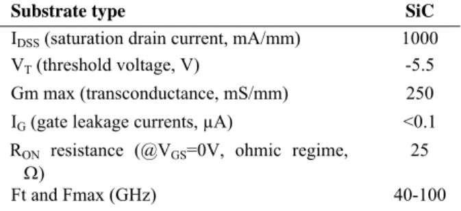
II.DEVICES ON SIC: SOME PERFORMANCES
The HEMT devices grown on silicon carbide substrate feature 24% aluminum content in the 2 DEG layer, and have been processed using the MOCVD technique [8]. Static and pulsed measurements have been largely performed respectively with HP4142 modular source and DIVA D225 system, on a large number of samples to appreciate the scattering of the electrical performances over the wafer.
Substrate type SiC
IDSS (saturation drain current, mA/mm) 1000
VT (threshold voltage, V) -5.5
Gm max (transconductance, mS/mm) 250 IG (gate leakage currents, µA) <0.1
RON resistance (@VGS=0V, ohmic regime,
Ω) 25
Ft and Fmax (GHz) 40-100
TABLE 1: HEMT (2x0.15x50 µm² gate area) static and dynamic parameters (mm unit refers to the normalization versus the gate width of the devices).
Scattering parameters measurements have been performed with HP8510 network vector analyzer. The main parameters are reported on Table 1 for devices featuring 0.15x2x50 µm² (and 0.25x2x75 µm²). These HEMT on SiC exhibit high drain current, high transconductance gain and low gate leakage current as
well as reduced contact or channel RON resistance,
revealing a good process maturity.
Device featuring 0.15x2x50 µm² is used for the study in the linear regime (for comparison with previous studies on silicon and sapphire substrates), while 0.25x2x75 µm² device is used for saturated regime study (LFN, and also residual phase noise and linear RF noise).
II.LOW FREQUENCY NOISE IN ALGAN/GANDEVICES
ON SICSUBSTRATES
In the next section, the study relates to the technological maturity level of the devices characterized under Ohmic biasing conditions. The second section of this paragraph is dedicated to the study under saturated biasing conditions.
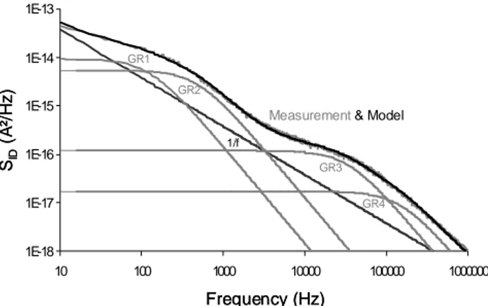
Figure 1 shows a typical drain current noise spectrum that evidence the presence of numerous trapping-detrapping centers (GR) and a flicker 1/f contribution. The closeness of the GR hinder their extraction, and analytical extraction procedure (MatLab) has been developed to get the different contributions of the noise parameters. The robustness of this procedure has been checked with analytical noisy spectra to ensure the uniqueness of the parameters convergence. More than 6 G-R centers, as well as flicker noise can be extracted over the considered frequency range. The extraction accuracy is just limited by the noise contribution weight in the overall noise (the weaker the noise contribution,
the worse the accuracy). The recomposed SID spectrum is
shown on figure 1. 1E-18 1E-17 1E-16 1E-15 1E-14 1E-13 10 100 1000 10000 100000 1000000 Frequency (Hz) SID (A ²/ H z ) GR1 GR2 GR3 GR4 1/f
Measurement& Model
1E-18 1E-17 1E-16 1E-15 1E-14 1E-13 10 100 1000 10000 100000 1000000 Frequency (Hz) SID (A ²/ H z ) GR1 GR2 GR3 GR4 1/f
Measurement& Model
Fig. 1. Extracted low frequency noise sources and overall spectrum (0.25x2x75 µm² HEMT @ VGS=-2 V, VDS=16 V)
Measurements are performed in the 10Hz-1MHz range using the transimpedance amplifier technique [9]. This
setup allows drain and gate spectral densities (resp. SID
and SIG), as well as cross-correlation measurements. The
correlation is found to be null, and SIG contribution is
very low due to weak leakage currents.
A. LFN under Ohmic regime in AlGaN/GaN HEMT
Figure 2 illustrates a drain current noise spectrum composed with 3 GR centers and a flicker noise source.
1E-21 1E-20 1E-19 1E-18 1E-17 1E-16 1E-15 10 100 1000 10000 GR1 GR2 GR3 1/f Frequency (Hz) SI D (A 2/H z )
Model &measurement
1E-21 1E-20 1E-19 1E-18 1E-17 1E-16 1E-15 10 100 1000 10000 GR1 GR2 GR3 1/f Frequency (Hz) SI D (A 2/H z )
Model &measurement
1E-21 1E-20 1E-19 1E-18 1E-17 1E-16 1E-15 10 100 1000 10000 GR1 GR2 GR3 1/f Frequency (Hz) SI D (A 2/H z )
Model &measurement
Fig. 2. Drain noise spectral density SID versus frequency
(measurement and model, with noise sources decomposition) @ VGS=-3.25 V, VDS=0.1 V
The 1/f flicker noise source seems to be correctly extracted from the upper frequency band where a slope of -1 appears. Spectral density’s levels for different bias conditions (in the linear Ohmic regime) are taken at 1 kHz, and reported on figure 3.
The Peransin’s technique [10] used in figure 3 is useful for devices comparison when biased in their linear zone. However, this technique is matched to devices that exhibit perfects 1/f spectra. The presence of GR has thus to be removed from the whole spectra in order to get the flicker contribution. From figure 3, we can see that the floor related to an operating mode where the noise and resistance contributions are located in the access resistances. The -3 slope behavior is also correctly extracted, but the -1 slope from theoretical expectation is not obtained, neither from direct measurements on the spectra, nor when removing GR influence.
1,E-15 1,E-14 1,E-13 1,E-12 1 1 -3 slope VGS=-3,25V 0 0 slope |VGS-VT| SI D /ID 2(H z -1) VGS=-2V -7 slope (out of band GR) 1,E-15 1,E-14 1,E-13 1,E-12 1 1 -3 slope VGS=-3,25V 0 0 slope |VGS-VT| SI D /ID 2(H z -1) VGS=-2V -7 slope (out of band GR)
Fig. 3. Normalized spectral density SID/ID² versus VGS @
1kHz, ▲ before removing GRs and ♦ after removing GRs
contribution.
This slope of -1 leads to the knowledge of the Hooge’s parameter (knowing the carriers sheet density and
mobility). However, a maximum value close to αH=5.10-5
has been extracted from a ‘worst case’ extrapolation study. This figure of merit puts this technology close to state of the art results.
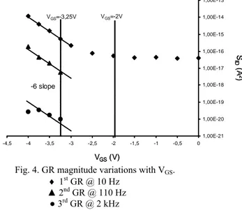
Figure 4 presents the variations of the 3 GR centers extracted in the linear zone appearing at constant frequencies of 10 Hz, 110 Hz and 2 kHz.
1,00E-21 1,00E-20 1,00E-19 1,00E-18 1,00E-17 1,00E-16 1,00E-15 1,00E-14 1,00E-13 -4,5 -4 -3,5 -3 -2,5 -2 -1,5 -1 -0,5 0 VGS(V) VGS=-3,25V S ID (A 2 ) VGS=-2V -6 slope 1,00E-21 1,00E-20 1,00E-19 1,00E-18 1,00E-17 1,00E-16 1,00E-15 1,00E-14 1,00E-13 -4,5 -4 -3,5 -3 -2,5 -2 -1,5 -1 -0,5 0 VGS(V) VGS=-3,25V S ID (A 2 ) VGS=-2V -6 slope
Fig. 4. GR magnitude variations with VGS.
♦ 1st GR @ 10 Hz
▲ 2nd GR @ 110 Hz
● 3rd GR @ 2 kHz
The dependence of these GR magnitudes with gate-source biasing exhibits a constant value from 0 V to -3 V for the GR at 10 Hz (which weight to the overall spectra hide the GR centers at 110 Hz and 2 kHz). When the
device is pinched below VGS= -3 V, the GR magnitudes
increase with a -6 slope. The GR magnitude featuring the lower weight is more sensitive to extraction uncertainty.
The non-realistic -7 slope trend from figure 3 can thus be related to the -6 slope issued from GR magnitude
dependence with VGS (and to -1 slope from the 1/f). It is
assumed that out of band (in the upper frequency band) GR centers must enhance the spectra shape, and then the extracted 1/f flicker noise source. The only way to check experimentally this hypothesis is to broaden the upper frequency range, but the bias tee on the drain access limits our experimental setup.
The next section point out that these GR centers are already present when devices are biased in the saturated regime, added with more complex noise behavioral phenomena.
B. LNF under saturated regime in AlGaN/GaN HEMT
Up to 7 different noise sources (1/f, GR) are needed to
fit the spectra when moving VDS and VGS biasing
voltages (Figure 5). 1E-19 1E-18 1E-17 1E-16 1E-15 1E-14 1E-13 10 100 1000 10000 100000 1000000 1/f behavior extracted 1/f Frequency (Hz) SID (A /H z ) 1E-19 1E-18 1E-17 1E-16 1E-15 1E-14 1E-13 10 100 1000 10000 100000 1000000 1/f behavior extracted 1/f Frequency (Hz) SID (A /H z )
Fig. 5. SID noise spectral density (VGS=-3 V, VDS=16 V) of
a 0.25x2x75 µm² gate width transistor.
Firstly, we notice that the GR frequencies shift with the biasing conditions. From the frequency-magnitude
evolution versus VDS at VGS=0V, thermal dependence of
3 GR centers (upper freq. band) are modeled. The thermal dependence of these centers is taken into account when the gate-source voltage varies (at a constant carrier density). The 3 low frequencies GR centers appear when pinching the device while the 3 higher frequencies GR centers shift with thermal dissipated power (ID.VDS). The
3 GR that appear with VGS seem to depend on the
quasi-Fermi level position, and to some surface or volume defect (respectively at the AlGaN/GaN layer or in the 2DEG). The defects responsible for such a GR pollution on the LFN spectra are not yet fully identified, but H+ seems to be present in high concentration levels [11] in the active layers.
We can also notice from figure 5 the quasi 1/f behavior in the 70 Hz-2 kHz range. This justify why LFN measurements must always be done on the widest frequency range as possible.
III.RESIDUAL PHASE NOISE AT 10GHZ
The LFN conversion around the carrier is a well established phenomenon, even if the noise RF floor can also play a strong contribution to the overall converted noise, especially for frequencies far from the carrier. The following graph (figure 6) is related to the residual phase noise [12] at a 10 GHz frequency on a 0.25x2x75 µm² gate area device. The transistor is used in its amplification mode and is loaded onto 50Ω. The input power issued from the high spectral purity source is -10 dBm, and the HEMT runs in its small signal regime. The measurements actually correspond to the phase
fluctuation of the S21 parameter around the 10 GHz
carrier. -160 -155 -150 -145 -140 -135 -130 -125 -120 -115 -110 10 100 1000 10000 100000 Frequency (Hz) R e s idu al p has e noi se ( d B ra d ²/ H z ) VGS=-3V, -2V, -1V -1 slope -2 slope
Fig. 6. Residual phase noise of a 0.25x2x75 µm² gate width transistor @ 10 GHz (VDS=10 V, VGS varies).
It can be noticed in Figure 6 that, up to 100 kHz offset frequency, an excess noise contribution dominates the transistor phase noise. This is typical of a phase noise spectrum of III-V field effect devices such as AlGaAs/GaAs or GaInAs/GaAs HEMTs, and the result in absolute value is even better than the phase noise level measured on some of these devices.
The measured phase is the result of a LFN conversion, which involves both 1:f and GR noise contributors. The phase noise is not totally correlated to the LFN, because
different LFN sources and different conversion phenomena are probably involved in the phase noise generation process. However, the general shape are the same.
Once again also, the noise behavior is largely dependent on the gate bias (GR “bulger” at the upper offsets). Further investigations will also include the phase noise dependence on the microwave power.
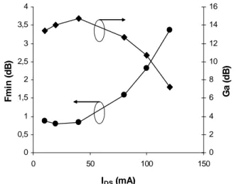
IV.LINEAR HIGH FREQUENCY NOISE
The experimental setup is based on the multi-impedance technique which is not well suited for broadband characterization because of stability problems according to the source reflection coefficient presented at the device’s input. However, we propose a specific reflection coefficient constellation for each frequency to avoid any instability. An optimum minimum noise figure
of Fmin=0.80dB is found at 8 GHz for a device featuring
2x75µm gate width biased at VDS=10 V, IDS=20 mA as
shown on figure 7. 0 0,5 1 1,5 2 2,5 3 3,5 4 0 50 100 150 IDS (mA) F m in ( d B ) 0 2 4 6 8 10 12 14 16 Ga ( d B ) 0 0,5 1 1,5 2 2,5 3 3,5 4 0 50 100 150 IDS (mA) F m in ( d B ) 0 2 4 6 8 10 12 14 16 Ga ( d B )
Fig. 7. Minimum noise figure and associated gain of a 0.25x2x75 µm² gate width transistor @ 8 GHz (VDS=10 V, VGS
varies from 0 V to -4.5 V).
The equivalent noise resistance Rn is found to be 32 Ω and the optimum reflection coefficient’s (Γopt) magnitude and phase are respectively of 0.70 and 31°. The associated gain is 14 dB. These figures agree with results issued from devices featuring quite the same area on silicon substrate [2]. More results will be proposed during the oral presentation.
V.CONCLUSION
HEMT devices grown on SiC substrate have been largely characterized under static and dynamic conditions. These results can be correlated to that issued from many authors contributions putting forward the advantage of these technologies for power applications in transmitter’s systems. Moreover, non-linear noise (low frequency noise and residual phase noise) and linear high frequency noise have been realized. The presence of GR
centers will enhance the noise around the carrier, thus degrading the spectral purity that should be obtained with a single 1/f behavior. Once these GR centers removed, this technology will set at a state of the art level. So these devices stand as good candidates for frequency synthesis, taking also benefit from a higher output power (thus avoiding any buffer amplifier for mixer’s gain conversion optimization). The linear RF noise feature
favorable characteristics (Fmin) for LNA’s design up to X
band. This extensive noise characterization assesses the pertinence for using AlGaN/GaN HEMT for integrated transceiver modules.
d CRHEA (CNRS laboratory) for providing the devices.
[1]
hniques, Vol. 53, No. 2,
[2] AS Symposium, [3] IMS [4] AS Symposium, [5] , Vol. 5470, [6]
Symposium, Amsterdam, Netherlands, 2004,
pp.159-[7]
substrates” proceedings [8]
ications” in [9]
Vol. 5470, Maspalomas, Spain, May
[10] n Devices, vol. 37, No 10, [11] res”, MRS-[12] ory and Technique Symposium Digest 2001, pp. 831-833.
ACKNOWLEDGEMENT
This work is supported by the French Ministry of Research under RNRT’s financial project (ANDRO). The authors specially want to thank Picogiga International Company an
REFERENCES
C. Sanabria et Al, “Influence of epitaxial structure in the noise figure of AlGaN/GaN HEMTs” IEEE Trans. on
Microwave Theory and Tec February 2005 , pp. 762-769.
A. Minko et Al, “RF noise and power performances of AlGaN/GaN on Si(111) substrates” 12th
GA Amsterdam, Netherlands, 2004, pp. 67-70.
H. Xu et Al., “Low phase-noise 5 GHz AlGaN/GaN HEMT oscillator integrated with BaxSr1-xTiO3 thin films”
Symposium, Forth Worth, U.S.A, 2004, pp. 1509-1512.
D. Krausse et Al., “Robust GaN HEMT low-noise amplifier MMICs for X-band applications” 12th
GA Amsterdam, Netherlands, 2004, pp. 71-74.
J.G. Tartarin et Al., “Using low frequency noise characterization of AlGaN/GaN HEMT as a tool for technology assessment and failure prediction”, Noise in
Devices and Circuits II, Proc. of SPIE Maspalomas, Spain, May 2004, pp.296-306.
G. Soubercaze-Pun et Al., “Carrier’s transport mechanisms investigations in AlGaN/GaN HEMT thanks to physical modelling and low frequency noise characterization”, 12th
GAAS 162.
J.G. Tartarin et Al., “Low frequency noise of AlGaN/GaN HEMT grown on Al2O3, Si and SiC
of ICNF, Salamanca, Spain, 2005.
M-A. di Forte-Poisson et Al., “MOCVD growth of group III nitrides for high power, high frequency appl
Phys. Stat. Sol. (c) 2, No. 3, 2005, pp. 947-955.
L. Bary et Al., “Low frequency noise behavior in GaN HEMTs on silicon substrate” Noise in Devices and Circuits
II, Proc. of SPIE, 2004, pp.286-295.
J.M. Peransin et Al., “1/f noise in MODFET’s at low drain bias” IEEE Trans. on Electro
October 1990, pp. 2250-2253.
J.M Arroyo et Al., “Effect of Deuterium diffusion’s on the electrical properties of AlGaN/GaN heterostructu
symposium E March 2005, San Francisco, USA.
O. Llopis et Al., “Non linear noise modeling of a PHEMT device through residual phase noise and low frequency noise measurements” IEEE Microwave The