UNIVERSITÉ DE MONTRÉAL
PROCESSING AND PATTERNING OF CONDUCTING POLYMER FILMS FOR FLEXIBLE, STRETCHABLE AND HEALABLE ELECTRONICS
SHIMING ZHANG
DÉPARTEMENT DE GÉNIE CHIMIQUE ÉCOLE POLYTECHNIQUE DE MONTRÉAL
THÈSE PRÉSENTÉE EN VUE DE L’OBTENTION DU DIPLÔME DE PHILOSOPHIAE DOCTOR
(GÉNIE CHIMIQUE) NOVEMBRE 2017
UNIVERSITÉ DE MONTRÉAL
ÉCOLE POLYTECHNIQUE DE MONTRÉAL
Cette thèse intitulée :
PROCESSING AND PATTERNING OF CONDUCTING POLYMER FILMS FOR FLEXIBLE, STRETCHABLE AND HEALABLE ELECTRONICS
présentée par: ZHANG Shiming
en vue de l’obtention du diplôme de: Philosophiae Doctor a été dûment acceptée par le jury d’examen constitué de:
M. AJJI Abdellah, Ph. D., président
M. CICOIRA Fabio, Ph. D., membre et directeur de recherche
Mme SANTATO Clara, Doctorat, membre et codirectrice de recherche M. SAVADOGO Oumarou, D. d'état, membre
DEDICATION
ACKNOWLEDGEMENTS
I am grateful for all the support, guidance and help that I have received over the last 4 years at Polytechnique Montreal.
First, I would like to express my deepest thanks to my research director, Prof. Fabio Cicoira, for giving me the opportunity to work in the field of organic bioelectronics. Thank you for guiding, supporting, and encouraging me during my study in Montreal. Your passion for science and your personal involvement in my projects helped me to overcome many difficult moments. Thank you for offering me freedom on the projects, for putting so much confidence in me, and for entrusting me. Thank you for always be available to discuss the projects with me. Thank you for your concerns and what you have done on my family issues in the past four years, for which I will always be grateful. No success will be there without your continuous care of me.
I am thankful to my co-supervisor, Prof. Clara Santato, for her advices and moral support. Her patience and laboratory space were invaluable for my projects. Thank you for your encouragement and your support on me. I will always be grateful for your special care of my family.
I am grateful to the jury members, Prof. Abdellah Ajii, Prof. Oumarou Savadogo, Prof. Frédéric Lesage, Prof. Frédéric Sirois, and Prof. Darren Lipomi, for their time and interest in my work. I am very grateful to NSERC for financial support through a Vanier Canada Graduate Scholarship, which motived me to set high standard for myself every single day.
Many thanks to all the collaborators, to John DeFranco of Orthogonal Inc. for discussions on the orthogonal photolithography, to Prof. Peter Grutter of McGill University for his invaluable input on the AFM/EFM characterizations on the stretchable electronics project, and his Ph.D. student Maddy Anthonisen for performing the AFM/EFM measurements and the useful discussions. I am also grateful to Keith Lewis, from SCS coating, for valuable instructions on Parylene deposition, to William Doak of Binghamton University on the design of tensile tester for the stretchable project, and to Richard Silverwood at Polytechnique for tensile tester measurements.
I am grateful to my all friends. Thanks Dr. Huiliang Wang (Stanford Univ) for input on the elastomer processing, Dr. Pei He (Manchester Univ) and Dr. Qingyu Cui (Michigan Univ) for endless discussions on the flexible devices, Qian Li (Youxin Pai Inc) for the time spent with me on the schematic image drawing, and Bo Zhang (Zhiyuan Electronics co., ltd.) for discussions and
design on the wireless communication devices. Thank Changsheng, Qinghua, Yinghao, Mengjiao, Hongliang for being my intimate friends in Polytechnique/UdeM.
I also want to thank some distinguished scientists for individual discussions at the conference which greatly inspired me. These thanks goes to Prof. Stephanie P. Lacour (EPFL), Prof. Zhenan Bao (Stanford Univ), Prof. Yonggang Huang (Northwest Univ), and many other scientists I met in the past years for invaluable discussions.
I am very grateful to technicians at Polytechnique: Daniel Pilon for his kind support on the Labview software for the device characterization, Christophe Clément and Alireza H. Mesgar for technical assistance in the clean room, and numerous discussions on my microfabrication issues, Josianne Lefebvre (XPS and ToF-SIMS), Nicole MacDonald (SEM), and Samir Elouatik (FTIR).
I have not yet thanked my colleagues at Polytechnique. I have to thank Gaia, Prajwal, Irina, Yang, Arun, Yasmina, Michelle, Tom, Come, Elizabeth, Shalin, Fanny, Camille, Hao, Olga, Laurie, Amel, Gabriel; and Francis, Frédéric, Eduardo, Zhaojing, Tian, Xu, Martin, Dominic, Guido, Tania, Jonathan, Julia, Sareh, and Dilek. It was a pleasure to work with you all. I enjoyed the time I spent with you in Montreal. I should be very grateful to life and to the chance I had to meet you. And many thanks to Polytechnique Montreal for academic and administrative services.
Finally, I would like to thank my father Weijun Zhang, my mother Jingfang Xie, my brother Shidong Zhang and his family, for their support and for always being with me.
RÉSUMÉ
L'électronique flexible, étirable et autoréparante a le potentiel de redéfinir l'apparence, la conception et la fabrication des appareils électroniques ayant un impact sur l'électronique personnelle, la peau électronique et les soins de santé. Le développement de l'électronique flexible, étirable et autoréparante à des fins biologiques et médicales fait appel à la biocompatibilité et la transparence des matériaux électroniques adaptable. Parmi ces matériaux, les polymères organiques conducteurs présentent des opportunités uniques. La recherche sur les propriétés électroniques, chimiques et mécaniques des polymères organiques conducteurs permet d’assurer leur intégration dans les appareils électroniques adaptable.
Cette thèse explore le traitement des polymères organiques conducteurs et le développement de nouvelles technologies de fabrication pour l'électronique flexible, étirable et autoréparante.
Nous avons premièrement recherché les effets de plusieurs additifs sur les propriétés fondamentales du polymère conducteur poly(3,4-éthylènedioxythiophène) polystyrène sulfonât (PEDOT:PSS). Nous avons démontré que les additifs jouent des rôles vitaux dans la détermination de la conductivité électronique de la couche mince, les propriétés mécaniques et la stabilité dans l'eau (essentielle aux applications biologiques). Nous avons trouvé que les couches minces déposées sur des substrats flexibles en plastiques ou sur des élastomères étirables démontrent une stabilité accrue dans l'eau en comparaison avec les couches minces sur des substrats rigides en verre. Des couches minces de PEDOT:PSS hautement conductrices, étirables et stables dans l'eau ont été obtenues en ajustant la composition chimique des couches et en contrôlant les conditions de traitement.
Pour la fabrication de dispositifs flexibles et étirables, un défi majeur apparait lors de la génération de patron de matériaux électroniques organiques dans le but de produire une électronique à haute résolution. L'application de la photolithograpie à cet effet n'est pas aussi facile, car les composés chimiques utilisés dans cette technique (photorésines, développeurs, décapant de résine) peuvent contaminer ou solubiliser les polymères organiques conducteurs. De plus, la génération de patrons d’électrodes métalliques pour les électroniques souples crée aussi un défi. En effet, l'adhésion des photorésines sur la surface des substrats souples (tels que les élastomères) sur lesquels les composants électroniques sont déposés est faible.
Nous avons pu fabriquer, avec une résolution micrométrique, des dispositifs qui peuvent soutenir des plis et des extensions afin de leur permettre de s'adapter à des surfaces courbées, souples et
élastiques. À cet effet, nous avons utilisé une photorésine récemment développée, qui est immiscible avec des matériaux organiques, pour générer des patrons de PEDOT:PSS. Des masques basés sur des couches minces (2 µm) de polymère ont été utilisées pour générer des patrons d’électrodes métalliques.
Ensuite, nous avons utilisé ces techniques pour fabriquer des transistors électrochimiques flexibles et étirables avec une résolution micrométrique. Nos dispositifs ont démontré une haute performance sous des conditions de pli et d'étirement et aussi une très bonne stabilité cyclique. Les dispositifs électroniques souples doivent supporter la déformation mécanique à travers le temps, qui peut endommager les appareils et nuire à leur fonctionnalité. Le développement de matériaux autoréparants, pouvant restaurer la fonctionnalité de l'appareil après endommagement, permettrait d’améliorer grandement la longévité de l'électronique souple. En particulier, l’autoréparation des matériaux électroniques organiques est de première importance car elle peut être combinée avec la flexibilité et la biocompatibilité. Ainsi, cette propriété est très prometteuse pour la détection biologique, l'enregistrement neurologique et l’ingénierie tissulaire.
Nous avons exploré les propriétés d’autoréparation du PEDOT:PSS. Les couches de PEDOT:PSS, avec une épaisseur de plus de 1 µm, démontrent une autoréparation électronique instantanée après que de l'eau ait été appliquée à l'endroit endommagé. Le processus d’autoréparation des couches minces n'est pas affecté par le dommage répété et se réalise très rapidement après mouillage. L’autoréparation se fait même après exposition à la vapeur d'eau. Nous avons établi qu’une application possible pour les couches minces autoréparantes est de les utiliser dans des détecteurs d’eau ultrasensibles.
La fabrication avancée et les techniques de traitements étudiées dans cette thèse permettront de paver la voie pour le développement de microélectroniques organiques souples pour les appareils électroniques portatifs et de stockage d'énergie flexibles, les écrans flexibles et les détecteurs d'humidité. En particulier, le fait que les appareils puissent travailler de manière stable et s'auto réparer dans l'eau, mène à de futures applications dans la détection biologique, les interfaces neurales, l'administration de médicaments et l'ingénierie tissulaire.
ABSTRACT
Flexible, stretchable and healable electronics have the potential to redefine the appearance, design and fabrication of electronic devices, with a profound impact on personal electronics, electronic skin and healthcare. The development of flexible, stretchable and healable electronics, in particular for biological or healthcare applications, calls for biocompatible, transparent and conformable electronic materials, among which organic conducting polymers present unique opportunities. Investigation of the fundamental properties of organic conducting polymers, in order to control their electronic, chemical and mechanical properties is therefore of great importance for their integration into conformable organic electronic devices.
This thesis explores the processing of organic conducting polymer and the development of new fabrication technologies for flexible, stretchable and healable electronics.
We first investigate the effect of several additives on the fundamental properties of the conducting polymer, poly(3,4-ethylenedioxythiophene) polystyrene sulfonate (PEDOT:PSS). We demonstrate that the additives play vital roles in determining the films’ electronic conductivity, mechanical properties, and water stability (essential for biologic applications). We find that films on flexible plastic and stretchable elastomer substrates show enhanced water stability compared with that of films on rigid glass substrates. Highly conductive, intrinsically stretchable and water-stable PEDOT:PSS thin films are finally obtained by adjusting the films’ chemical composition and controlling the processing conditions.
For the fabrication of flexible and stretchable device, a major challenge is the patterning of organic electronic materials to produce electronics with high resolution. Applying conventional photolithographic techniques to this purpose is not straightforward, because the standard lithography chemicals (photoresists, developers, strippers) may contaminate or solubilize the organic material. In addition, the patterning of metallic electrodes for soft electronics is also challenging because photolithography is an inefficient method for directly patterning stretchable electronics, due to the poor adhesion of the photoresist on the surfaces of soft substrates (such as elastomers) on which electronic components are deposited.
We are able to pattern devices with microscale resolution that are able to sustain not only bending but also extensive stretching, so that they can accommodate on curved, soft, and elastic surfaces. To this purpose we use a recently developed photoresist, which is non-miscible with organic
materials, to pattern PEDOT:PSS and a ultrathin polymer film (< 2 µm) to pattern metallic electrode arrays on stretchable substrates. We use these technologies thereafter to develop both flexible and stretchable organic electrochemical transistors with microscale resolution. Our devices show high performance with unchanged electrical properties under extreme bending or stretching conditions, and also superior cyclic stabilities.
Soft electronics must endure mechanical deformation over time, which may damage devices and disable their functionality. The development of healable materials, which can repair themselves and restore the device functionality after damage could greatly improve the longevity of soft electronics. Particularly, healing of organic electronic materials is of primary importance because it can be combined with flexibility and biocompatibility, thus being very promising for long-term biological sensing, neurologic recording and tissue engineering applications.
We explore the healing property of PEDOT:PSS. PEDOT:PSS films (with thickness greater than 1 µm) show instantaneous electronic healing after water is applied to the damaged area. The healing process of the films is not affected by repeated damage to the film and occurs very rapidly, i.e. within 150 ms after wetting. Healing occurs even after exposure to water vapor. The potential of healable PEDOT:PSS thin films is demonstrated as ultrasensitive water detectors and as active materials for self-healing organic electronic devices.
The advanced fabrication and processing technologies investigated in this thesis pave the way for the development of soft organic microelectronics for personal wearable electronics, flexible energy storage devices, flexible display and humidity detectors. In particular, the fact that devices can work stably and can self-repair in water leads to further applications in biological sensing, neural interfaces, drug delivery, and tissue engineering.
TABLE OF CONTENTS
DEDICATION ... III ACKNOWLEDGEMENTS ... IV RÉSUMÉ ... VI ABSTRACT ... VIII TABLE OF CONTENTS ... X LIST OF FIGURES ... XIV LIST OF ABBREVIATIONS ... XX LIST OF SYMBOLS ... XXII LIST OF APPENDICES ... XXIVCHAPTER 1 INTRODUCTION AND OBJECTIVES ... 1
1.1 Organic electronics and organic bioelectronics ... 1
1.2 Motivations and objectives of this thesis ... 2
CHAPTER 2 LITERATURE REVIEW ... 5
2.1 Why some polymers conduct electricity ... 6
2.1.1 Chemical bonds in conducting polymer ... 6
2.1.2 Electron delocalization in conjugated backbones ... 7
2.1.3 Doping is the key ... 7
2.2 The conducting polymer PEDOT:PSS ... 8
2.3 PEDOT:PSS processing ... 10
2.3.1 Electrical conductivity ... 10
2.3.2 Film forming properties ... 13
2.3.3 Flexibility and stretchability ... 14
2.4 PEDOT:PSS patterning ... 17
2.5 The transistor ... 18
2.5.1 Field-effect transistor ... 19
2.5.2 Electrochemical transistor ... 19
2.6 Organic electrochemical transistors (OECTs) ... 21
2.7 Figures of merit of OECTs ... 22
2.7.1 Transfer and output characteristics ... 22
2.7.2 ON/OFF ratio ... 22
2.7.3 Transconductance ... 23
2.7.4 Response time ... 23
2.7.5 Mobility ... 24
2.8 Applications of organic electrochemical transistors (OECTs) ... 25
2.8.1 Non-faradic sensing ... 25
2.8.2 Faradic sensing ... 26
2.8.3 Cell sensing and in vivo recording ... 27
2.9 Strategies for stretchable electronics ... 28
CHAPTER 3 ARTICLE 1: SOLVENT-INDUCED CHANGES IN PEDOT:PSS FILMS FOR ORGANIC ELECTROCHEMICAL TRANSISTORS ... 31
3.1 Authors ... 31
3.2 Abstract ... 31
3.3 Introduction ... 31
3.4 Experimental part ... 33
3.5 Results and discussions ... 33
3.6 Conclusion ... 40
CHAPTER 4 ARTICLE 2: WATER STABILITY AND ORTHOGONAL PATTERNING
OF FLEXIBLE MICRO-ELECTROCHEMICAL TRANSISTORS ON PLASTIC ... 42
4.1 Authors ... 42
4.2 Abstract ... 42
4.3 Introduction ... 42
4.4 Results and discussions ... 44
4.5 Conclusion ... 49
4.6 Materials and Methods ... 49
4.7 Acknowledgements ... 50
CHAPTER 5 ARTICLE 3: PATTERNING OF STRETCHABLE ORGANIC ELECTROCHEMICAL TRANSISTORS ... 51
5.1 Authors ... 51
5.2 Abstract ... 51
5.3 Introduction ... 51
5.4 Results and discussion ... 53
5.5 Conclusion ... 58
5.6 Experimental section ... 59
5.7 Acknowledgement ... 62
CHAPTER 6 ARTICLE 4: WATER-ENABLED HEALING OF CONDUCTING POLYMER FILMS ... 63
6.1 Authors ... 63
6.2 Abstract ... 63
6.3 Introduction ... 64
6.4 Results and discussion ... 65
6.6 Acknowledgments ... 76
CHAPTER 7 GENERAL DISCUSSION ... 77
CHAPTER 8 CONCLUSION AND RECOMMENDATIONS ... 80
BIBLIOGRAPHY ... 83
APPENDICES ... 94
LIST OF FIGURES
Figure 2.1. Chemical structures of some conducting polymers13. Reprinted with permission. ... 6 Figure 2.2. (A) Illustration of π bond and σ bond, and (B) the energetic difference of the π bond and the σ bond, in Trans-Polyacetylene16. ... 7
Figure 2.3. A demonstration of the electrical conductivity of conducting polymers. (A) Dopants add an electron to (or remove it from) the polymer chain, thus creating a delocalized charge. (B) It is energetically favorable to localize this charge and surround it with a local distortion of the crystal lattice. (C) A charge surrounded by a lattice distortion is called a polaron (a radical ion associated with a lattice distortion). (D) The polaron is able to travel freely along the polymer chain, leading to a conductive increase17. Reprinted with permission. ... 8
Figure 2.4. Chemical structure of PEDOT:PSS. The positive charges on the PEDOT chain are compensated for by negative sulphonate ions on the PSS chain19. Reprinted with permission.
... 9 Figure 2.5. Several applications of the commercial Haraeus CleviosTM PEDOT:PSS products23. 10 Figure 2.6. Improved conductivity of H2SO4-treated PEDOT:PSS due to removal of 70% PSS (100%
H2SO4) and formation of well-crystallized PEDOT nanofibrils34. Reprinted with permission.
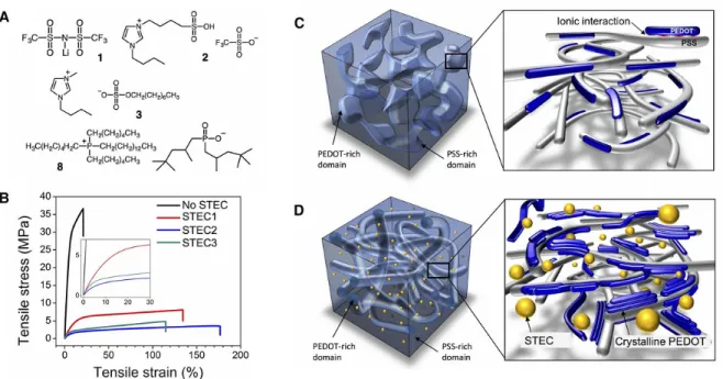
... 12 Figure 2.7. Commonly described microstructure of PEDOT:PSS (a) PEDOT synthesis on PSS template, (b) formation of colloidal gel particles in dispersion and (c) resulting film with PEDOT:PSS-rich (blue) and PSS-rich (grey) phases. (d) Aggregates/crystallites support enhanced electronic transport21. Reprinted with permission. (e) The typical diameter of PEDOT/PSS grains is 40–60 nm, with a PSS-rich shell thickness of 5–10 nm36. Reprinted with permission. ... 13 Figure 2.8. Additives used to improve specific properties of PEDOT:PSS. ... 14 Figure 2.9. Chemical structures and schematic representation. (A) Representative stretchability and electrical conductivity enhancers. (B) Strain-stress curves of PEDOT:PSS with and without stretchability and electrical conductivity (STEC) enhancers. (C and D) Schematic diagram
representing the morphology of (C) a typical PEDOT:PSS film versus that of (D) a stretchable PEDOT film with STEC enhancers30. Reprinted with permission. ... 16 Figure 2.10. The immiscibility of fluorous, aqueous, and organic liquids (shown above, left) enables patterning of two overlapping stripes of light-emitting polymers, with the use of a fluorinated photoresist (shown above, right)61. Reprinted with permission. ... 18 Figure 2.11. Cross-sections of polymer EG transistors showing the difference between (a) electrostatic FET and (b) electrochemical doping ECT7. Reprinted with permission. ... 19 Figure 2.12. Proposed model of the double-layer region under conditions where anions are specifically adsorbed. The solution side of the double layer is thought to be made up of several “layers.” That closest to the electrode, the inner layer, contains solvent molecules and sometimes other species (ions or molecules) that are said to be specifically adsorbed. This inner layer is also called the compact, Helmholtz, or Stern layer. The locus of the electrical centers of the specifically adsorbed ions is called the inner Helmholtz plane (IHP), which is at a distance x1. The total charge density from specifically adsorbed ions in this inner layer is
σ1 (uC/cm2). Solvated ions can approach the metal only to a distance x2; the locus of centers
of these nearest solvated ions is called the outer Helmholtz plane (OHP)66. Reprinted with permission. ... 20 Figure 2.13. PEDOT:PSS-based OECTs. A conductive channel is formed for gate voltages that cause the PEDOT to be in the doped state (top). By reversing the gate potential, the PEDOT can be undoped by electrochemical reaction in the film, rendering the channel nonconductive (bottom). The ionic transport in and out of the film is facilitated by the gate electrode, either by charging and discharging of the EDL of the electrode (shown) or by electrochemical reactions67. Reprinted with permission. ... 22 Figure 2.14. a) Schematic of the device indicating the charge distribution around the dedoping front according to the model (not to scale), the drift length of injected ions, the total length, L, of the PEDOT:PSS film, and the area, A , of the electrolyte/conducting polymer junction42. Reprinted with permission. b) Experimental transient response of an OECT under application of a constant gate current71. Reprinted with permission. ... 25
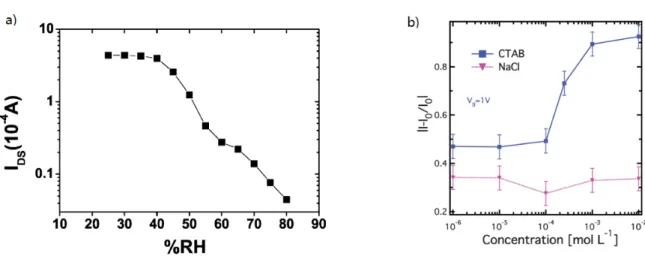
Figure 2.15. (a) Ids measurements in an OECT at variable relative air humidity73. Reprinted with
permission. (b) OECT modulation, where I is the OFF current and the I0 is the ON current (Vg= 0V), versus molar concentration of CTAB and NaCl aqueous solutions at Vg = 1 V74.
Reprinted with permission. ... 26 Figure 2.16. OECTs research progress towards cell sensing and in vivo recording70,83-90. ... 28 Figure 2.17. (a) Bulking method (out of plane): a schematic illustration of the process for building stretchable single-crystal Si devices on elastomeric substrates98; Reprinted with permission. And various geometric structuring methods to impart stretchability at different length scales using in-plane films: b) A percolating pathway in an Au film, consisting of micron-sized cracks under applied strain; c) A percolating pathway in a nanowire film; d) Out-of-plane deformation of a serpentine metal interconnect. Adapted with permission; and e) Distortion of a substrate patterned on the device level91. Reprinted with permission. ... 29
Figure 3.1. Electrical conductivity of PEDOT:PSS films processed from mixtures containing Clevios PH1000, 0.5 v/v % DBSA, and different v/v % concentrations of conductivity enhancing agents (DMSO, EG, glycerol). The inset shows the electrical conductivity variation versus increasing DBSA concentrations in absence of conductivity enhancing agents. The films thickness is about 150 nm. The error bars correspond to the standard deviations of three samples. ... 34 Figure 3.2. Thickness and conductivity of PEDOT:PSS films (after immersion for 10 minutes) versus polarity parameters of the solvents: isopropanol (polarity parameter 3.9), acetone (5.1), and Milli-Q deionized water (10.2). The value at polarity parameter =0 corresponds to the film thickness before immersion in the solvents. The thickness values on the left y axes are normalized with respect to the initial films thicknesses (about 150 nm). The PEDOT:PSS film is deposited from a mixture containing 94.5 v/v % of Clevios PH1000, 5 v/v % glycerol, and 0.5 v/v % DBSA. The polarity parameters are obtained from the literature125. The error bars correspond to the standard deviations of three samples. ... 36 Figure 3.3. XPS S(2p) spectra of films processed from mixtures containing 94.5 v/v% of CleviosTM PH1000, 5 v/v% glycerol and 0.5 v/v% DBSA after water immersion for 10 min: (a) without GOPS; (b) with 1 v/v % GOPS. ... 37
Figure 3.4. Thickness (left y scale) and conductivity (right y scale) change of films processed from mixtures containing 94.5 v/v% of CleviosTM PH1000, 5 v/v% glycerol and 0.5 v/v% DBSA with increasing GOPS concentration. The error bar stands for standard deviation of three samples. ... 38 Figure 3.5. Transient electrical measurement (10 cycles) with a duration of about 15 000 s (250 min) for OECTs fabricated from PEDOT:PSS/5 v/v % glycerol/0.5 v/v % DBSA films: (a) without GOPS; (b) with 1 v/v % GOPS. The spin-coating speeds for both films are 500 rpm for 10 s followed by 1500 rpm for 45 s. The thickness of the film with and without 1 v/v % GOPS is about 350 nm and 150 nm, respectively. ... 39 Figure 4.1. Scheme of the fabrication process of flexible OECTs: (a) photolithography patterning of gold electrodes on PET sheets laminated on PDMS/glass; (b) PEDOT:PSS spin-coating; (c) spin coating and photolithographic patterning of the fluorinated photoresist on PEDOT:PSS; (d) oxygen reactive ion etching of PEDOT:PSS and photoresist removal; (e) second photoresist pattern to protect the metal electrodes; (f) detachment of PET from PDMS/glass; (g) digital photograph of devices on a flexible PET foil and optical microscopy image showing the Au electrodes and the patterned PEDOT:PSS channel (the channel length/width is 5 µm/400 µm, the dark area between the two Au electrodes corresponds to the patterned PEDOT:PSS channel). ... 45 Figure 4.2. PEDOT:PSS films on glass and PET substrates after solvent immersion. (a) PEDOT:PSS/5% v/v glycerol/0.5% v/v DBSA on glass after 1 day in DI water; (b) PEDOT:PSS/5% v/v glycerol/0.5% v/v DBSA/1% v/v GOPS on glass after 3-month in DI water; (c) PEDOT:PSS/5% v/v glycerol on PET after 3-month in PBS; and (d) DI water. Films on glass that do not contain GOPS delaminate after 1 day of immersion in water, whereas those containing GOPS delaminate after about 3-month. Films on PET containing only PEDOT:PSS and glycerol do not delaminate even after 3-month in DI water or PBS. ... 46 Figure 4.3. (a) Normalized current versus film bending. The inset shows the schematic of bending test methods of the PEDOT:PSS films on PET. The bending percentage is defined as [(L − L ′)/L] × 100%. (b) Capacitance (left axis) and anodic charge (right axis) extracted from CV of films processed from PEDOT:PSS and 5% v/v glycerol. ... 47
Figure 4.4. Electrical characteristics of OECT on PET. (a) Output characteristics with Vds swept
from 0 V to −0.6 V and Vgs varying from 0 (top curve) to 0.8 V (bottom curve) with a step of
0.2 V. (b) Transfer curve for Vds = −0.6 V and Vgs sweeping from 0 to 0.8 V and the associated
transconductance. (c) Hysteresis curve for Vgs varying from 0 to 0.8 V at Vds = −0.2 V with
sweeping rate of 200 mV s−1. (d) Transient characteristics (Ids versus time) measured at a
fixed drain-source voltage (Vds) while pulsing for 2 seconds the gate-source voltage (Vgs) from
−0.2 to 0.8 V in 0.2 V steps. ... 48 Figure 5.1. Parylene transfer process used to fabricate microelectrode arrays on PDMS. (a) Detaching PET (CTAB-treated)-carried Parylene patterns from glass; (b) laminating of the PET/Parylene onto freshly prepared PDMS; (c) detaching PET, leaving Parylene patterns on PDMS; (d) metal deposition; (e) lift-off of the Parylene film; (f) electrode arrays on PDMS; (g) PDMS patterned with Au electrodes with substrate dimension of 15 mm × 15 mm; and (h) Au microelectrodes with channel lengths of 5, 20, and 50 µm. ... 54 Figure 5.2. Electrical characteristics of PEDOT:PSS micro-OECTs on PDMS. (a) Output (Vgs
varying from −0.2 to 0.8 V) and (b) transfer characteristics (Vds = −0.2 V) with associated
transconductance. Optical micrograph of the patterned OECT with channel width of 4000 µm, channel length of 10 µm, and channel thickness of about 400 nm (inset). The dark region corresponds to the patterned PEDOT:PSS film. ... 56 Figure 5.3. (a) Fabrication of stretchable OECT, using Parylene transfer and orthogonal patterning, carried out on 30% prestrained PDMS: (i) Prestretching PDMS substrate; (ii) Au patterning via Parylene transfer and PEDOT:PSS patterning via orthogonal photolithography; (iii) stretchable OECTs obtained upon PDMS relaxation; (iv) detachment of PDMS from glass substrate; (b) optical images of PEDOT:PSS and Au film surface morphology showing a transition from smooth to buckled morphology after release of prestretched PDMS; (c) prestretching effect on the stain-current profile of the PEDOT:PSS channel on PDMS; PEDOT:PSS films (with 5 % (v/v) glycerol and 1 % (v/v) Capstone FS-30) deposited on 30% prestretched substrate; d) transfer characteristics (Vds = −0.5 V) of stretchable OECTs at 0%,
15%, and 30% strains. The inset shows the schematic representation of our OECT configuration. The distance between the PEDOT:PSS gate and channel is 200 µm. The channel and the gate electrode are both 8 mm long and 2 mm wide. ... 58
Figure 6.1. Current versus time measurements (applied voltage 0.2 V) for PEDOT:PSS film (thickness: 10 µm; width: 4 mm; length: 20 mm) showing the effect of damage (cutting with a razor blade) and healing (covering the damaged area with a drop of water). The damage/healing process was repeated three times on different regions of the film. The inset shows the magnified image of the current response time to highlight the rapidity of the healing process. ... 66 Figure 6.2. SEM images of the damaged area of a PEDOT:PSS film (obtained adding 5 v/v.% glycerol to Clevios PH1000) before (a) and after (b) healing with a 10 µL drop of deionized water; c) schematic representation of water-induced mechanical and electrical healing of a PEDOT:PSS film (thickness: 10 µm; width: 4 mm; length: 20 mm); d) demonstration of the damage and healing effect on a PEDOT:PSS film connected in a circuit with a LED bulb at a constant voltage of 3 V: i) as-prepared intact film; ii) film damaged with a cut; iii) film healed by dropping DI water on the cut, which enables an immediate repair of the circuit (within 150 ms)... 67 Figure 6.3. Current versus time profile of wetted PEDOT:PSS film containing the conductivity enhancer glycerol (thickness: 10 µm; width: 4 mm; length: 20 mm) after several cuts in different areas of the film. The applied voltage was 0.2 V. The higher current with respect to Figure 6.1 is due to the presence of a conductivity enhancer. ... 69 Figure 6.4. Current versus time plot of PEDOT:PSS film containing the conductivity enhancer glycerol (thickness: 10 µm; width: 4 mm; length: 20 mm) measured in a humidity chamber with RH varying from 60% to 90%, at a constant voltage of 0.2 V. A complete current recovery was observed within 5 min after increasing the humidity to 80% RH and 90% RH. ... 70 Figure 6.5. a) Illustration of the water-assisted wedging method used to obtain free-standing PEDOT:PSS films, b) the film is detached from the glass substrate with tweezers, and c) does not deteriorate during the process. d) Excellent film conformability of PEDOT:PSS free-standing films (10 µm thickness) on finger and e) on fingertip. The fingerprint details are clearly visible in (e). ... 73
LIST OF ABBREVIATIONS
AC Activated carbonsAg Silver
AgCl Silver chloride Au Gold
BJT Bipolar junction transistor CE Counter electrode
CNT Carbon nanotube
CTAB Cetyltrimethylammonium bromide D Drain
DBSA Dodecyl benzene sulfonic acid DMSO Dimethyl sulfoxide
ECoG Electrocorticography ECT Electrochemical transistors EDL Electrical double layer EEG Electroencephalogram EG Electrolyte-gated
EIS Electrochemical Impedance Spectroscopy FET Field-effect transistor
G Gate
GOx Glucose oxidase
GOPS Glycidoxypropyltrimethoxysilane H2O2 Hydrogen peroxide
HFE Hydrofluoroethers
HOMO Highest occupied molecular orbital IL Ionic liquid
LED Light-emitting device
LUMO Lowest unoccupied molecular orbital
MOSFET Metal–oxide–semiconductor field-effect transistor NaCl Sodium chloride
OECTs Organic electrochemical transistors OLEDs Organic light-emitting diodes OTFTs Organic thin-film transistors OSCs Organic solar cells
PBS Phosphate-buffered saline PDMS Poly(dimethylsiloxane)
PEDOT:PSS Poly(3,4-ethylenedioxythiophene):polystyrenesulfonate PET Polyethylene terephthalate
PLGA Poly(L-lactide-co-glycolide) Pt Platinum
RE Reference electrode RIE Reactive ion etching S Source
SiO2 Silicon dioxide
STEC Stretchability and electrical conductivity WE Working electrode
LIST OF SYMBOLS
Ag Gate areaCc Channel capacitance per unit area
Cg Gate capacitance per unit area
C Capacitance Cr Chromium E Electrical field e- Electron G Transconductance Ids Source-drain current Ion ON-state current
Ioff OFF-state current
Ig Gate-source current Igs Gate-source current l Drift length K Boltzmann constant L Length M+ Cations n Electron density T Temperature t Time τe Transit time Ti Titanium u Mobility
v Velocity
V Voltage
Vds Drain-source voltage
Vg Gate-source voltage
Vgs Gate-source voltage
Vsol Gate voltage drop on the channel
LIST OF APPENDICES
Appendix A: SUPPORTING INFORMATION OF ARTICLE SOLVENT-INDUCED CHANCES IN PEDOT:PSS FILMS FOR ORGANIC ELECTROCHEMICAL
TRANSISTORS ... 97 Appendix B: SUPPORTING INFORMATION OF ARTICLE WATER STABILITY AND ORTHOGONAL PATTERNING OF FLEXIBLE MICRO-ELECTROCHEMICAL
TRANSISTORS ON PLASTIC ... 104 Appendix C: SUPPORTING INFORMATION OF ARTICLE PATTERNING OF
STRETCHABLE ORGANIC ELECTROCHEMICAL TRANSISTORS ... 108 Appendix D: SUPPORTING INFORMATION OF ARTICLE WATER-ENABLED
HEALING OF CONDUCTING POLYMER FILMS ... 116 Appendix E: LIST OF PUBLICATIONS AT POLYTECHNIQUE
MONTREAL NOT INCLUDED IN THE THESIS ... 125 Appendix F: PARTICIPATION TO CONFERENCES ... 126 Appendix G: SCHOLARSHIPS AND AWARDS RECEIVED AT
CHAPTER 1
INTRODUCTION AND OBJECTIVES
1.1 Organic electronics and organic bioelectronics
Organic materials have been traditionally considered as insulators. Therefore, most electronic devices, such as transistors or light emitting devices, for a long time have been exclusively based on inorganic materials. In the 1970s, the discovery that polymers can show electrical conductivity that can be increased up to seven orders of magnitude upon chemical doping, altered scientists’ understanding of organic materials1. This breakthrough observation was recognized by awarding Alan J. Heeger, Alan G. MacDiarmid and Hideki Shirakawa the Nobel Prize in Chemistry in 2000 “for the discovery and development of conductive polymers”. Since then, conductive polymers have become the cornerstone of a new type of electronics: organic electronics. Organic electronic materials have the advantages of light weight, superior flexibility, solution processability and biocompatibility2. These unique properties open new fields for applications such as flexible displays, flexible solar cells, wearable healthcare devices and disposable electronics2. One example, organic light-emitting diodes (OLEDs), has already entered the market for small-area displays and lighting applications3,4.
Inorganic electronic materials normally conduct only electronic charge carriers, while organic conducting polymers conduct both electronic and ionic charge carriers (mixed conduction)5. Since 2007, the mixed conduction behavior in organic conducting polymers has received great attention, especially for biological applications. The interplay between electronic and ionic signals, i.e., ion-to-electron conversion, is at the basis of the new field of organic bioelectronics6. Organic bioelectronics deal with devices operating at the interface between biology and human-made electronics, with possible applications in sensing, diagnostics and healthcare7.
Among the most exciting examples of organic bioelectronics devices are organic electrochemical transistors (OECTs). The first OECT, based on polypyrrole, was developed in 1984 by Wrighton’s group8. In 2002, a solution-processable and air-stable conducting polymer,
poly(3,4-ethylenedioxythiophene)-poly(styrene sulfonic acid) (PEDOT:PSS), was introduced as a channel material into OECTs9. Since then, dozens of groups across Europe, America, Asia and Australia have become active in OECT research10. Hundreds of peer-reviewed publications per year, along
with multiple international symposia, indicate both that the potential of OECTs has not been fully exploited and research on OECTs is in its infancy with many challenges still to be overcome.
1.2 Motivations and objectives of this thesis
Human body is soft, while electronics on silicon are not. Realizing soft electronic devices that overcome this fundamental mechanical mismatch will permit applications that are impossible to achieve with rigid devices. In addition, self-healing is a unique property of the human skin but is not attainable in most electronic materials. Self-healing electronic materials represent a very interesting and important area of research especially for soft electronics because soft electronic devices must endure mechanical deformation over time, which may damage devices and disable their functionality. In particular, healable OECTs will inarguably increase device longevity and improve long-term device reliability. Given the rapid growth of wearable electronics, establishing technologies for soft and healable OECTs will also promote their integration with such systems. The primary objective of this thesis is to develop flexible, stretchable and healable electronic materials and devices, e.g., OECTs, for applications in sensing, diagnostics and healthcare. In working towards this goal, it is of paramount importance to investigate the processing of conducting polymers to achieve flexibility, stretchability and healability and to develop new device fabrication technologies on substrates that are unconventional for electronics, such as polyethylene terephthalate (PET) and poly(dimethylsiloxane) (PDMS).
Therefore, the main specific objectives of this thesis are:
(1) Processing flexible, stretchable and healable PEDOT:PSS films. A better understanding of fundamental properties of PEDOT:PSS is essential to control device performance, and also of great fundamental interest for other research topics, since PEDOT:PSS is the most successful conductive polymer in terms of practical applications.
(2) Developing new technologies for patterning PEDOT:PSS and metallic electrode arrays on flexible and stretchable substrates, and fabricating flexible and stretchable micro-OECTs.
In Chapter 2, the history, working mechanism, figures of merit, and applications of OECTs are discussed. Chapter 2 also contains the introduction to PEDOT:PSS processing, with special attention paid to electrical and mechanical properties. Finally, the existing technologies for PEDOT:PSS patterning and research progress in flexible and stretchable OECTs are reviewed. Chapters 3 to 6 are reprints of four articles resulting from the work for this thesis.
-Article 1: Shiming Zhang, Prajwal Kumar, Amel Sarah Nouas, Laurie Fontaine, Hao Tang, Fabio Cicoira, Solvent-induced changes in PEDOT: PSS films for organic electrochemical transistors, APL Materials, 2015, 3 (1), 014911.
-Article 2: Shiming Zhang, Elizabeth Hubis, Camille Girard, Prajwal Kumar, John DeFranco, Fabio Cicoira, Water stability and orthogonal patterning of flexible micro-electrochemical transistors on plastic, Journal of Materials Chemistry C, 2016, C 4 (7), 1382-1385.
-Article 3: Shiming Zhang, Elizabeth Hubis, Gaia Tomasello, Guido Soliveri, Prajwal Kumar, Fabio Cicoira, Patterning of stretchable organic electrochemical transistors, Chemistry of Materials, 2017, 29 (7), 3126–3132.
-Article 4: Shiming Zhang and Fabio Cicoira, Water-enabled healing of conducting polymer films, Advanced Materials, 2017, DOI: 10.1002/adma.201703098.
In Article 1, we systematically study how additives affect film conductivity and identify glycerol as the best conductivity enhancer. We investigate film stability on glass and reveal a thickness loss after the sample is immersed in polar solvents. The thickness loss can be prevented by adding a crosslinking agent in the suspension before coating. Then, in Article 2, we observe that films processed on plastic PET substrates show better long-term water-stability than films on glass substrates. We perform orthogonal photolithography to pattern PEDOT:PSS on PET and fabricate flexible micro-OECTs featuring high performance and excellent water stability. In Article 3, we investigate the additives’ effect on film stretchability. By engineering a wrinkle device structure, introducing a new metallic micro-patterning method and using stretchable hydrogel as electrolyte, we assemble a fully stretchable organic transistor. In Article 4, we demonstrate that PEDOT:PSS can show electrical healing properties by increasing film thickness. The rapid-healing property is utilized to demonstrate a self-healing organic transistor and a wireless water detector.
In Chapter 8, the results of this thesis are discussed as a whole, supported by the literature review and the published articles. Finally, conclusions are drawn and perspectives on future work are given in Chapter 9.
CHAPTER 2
LITERATURE REVIEW
Nowadays, smart cellphones, flat panel displays, computers, sensors, memories and other electronic products play an indispensable role in daily life. Information display products link every corner of the world via internet and various electronic devices. In modern society, they are an ever-present extension of our corporeal fabric and help us to deal with a myriad of daily tasks. Key components inside these devices are semiconductor-based logic devices, such as complementary metal-oxide semiconductors (CMOSs) and bipolar junction transistors (BJTs) for high-speed logic calculation, field-effect transistors (FET) and light-emitting diodes (LED) for information processing and display11. For decades (1930s-1970s) these devices have been based on inorganic materials, which show high performance, high stability and, importantly, can be processed with mature fabrication technologies.
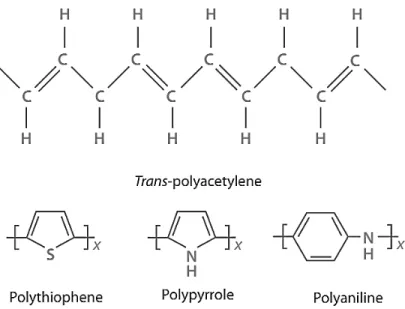
Generally speaking, polymers are insulators. In 1977, Alan J. Heeger, Alan G. MacDiarmid and Hideki Shirakawa discovered that conductivity of the semiconducting polymer polyacetylene can increase seven orders of magnitude upon oxidization (reaching the order of 103 S/cm1) by exposing it to halogen. This breakthrough observation was recognized by the Nobel Prize in Chemistry for 2000 “for the discovery and development of conductive polymers”. The combination of metal and polymer properties in a conducting polymer opens new opportunities in many applications, particularly in the electronics industry. In addition, conducting polymers are generally not thermoplastics and do not melt at high temperatures. Since 1977, conducting polymers have become the cornerstone of a new type of electronics: organic electronics12. In addition to polyacetylene, a series of conducting polymers, including polythiophene, polypyrrole, and polyaniline13 (Figure. 2.1), and the low-energy-gap light-emitting polymers polyphenylene vinylene were reported from the 1970s to 1980s14, which greatly promoted research on organic electronics.
Figure 2.1. Chemical structures of some conducting polymers13. Reprinted with permission.
2.1 Why some polymers conduct electricity
2.1.1 Chemical bonds in conducting polymer
The general electronic configuration of conducting polymer trans-polyacetylene is 1s2, 2s2 2p2, the ground state electronic configuration of carbon is 1s2, 2s2 2px12py12pz0, and the excited state
electronic configuration of carbon is 2s1 2px12py12pz1. The 2s1 and 2px1, 2py1 orbitals of carbon
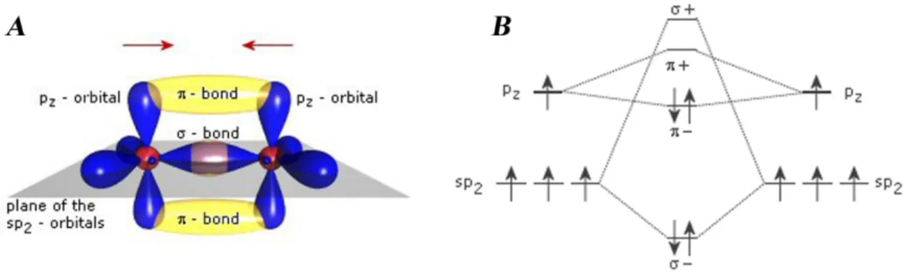
undergo sp2 hybridizations and form three sp2 hybrid orbitals in a planar structure (Figure. 2.2), the three sp2 hybrid orbitals and one pure 2pz1 orbital having one electron each. In polyacetylene, σ
(sp2-sp2) bonds are observed between two adjacent carbon atoms15. The remaining one pure 2pz1
orbital of one carbon atom overlaps sideways with the corresponding 2pz1 orbital of another carbon
atom and thus forms one π bond16 (Figure. 2.2). According to energy bond theory, the energy difference between the occupied binding orbitals and the unoccupied anti-binding orbitals of the σ bonds is quite large and well beyond the visible spectral range. Correspondingly, they have a large gap between the highest occupied molecular orbital (HOMO) and the lowest unoccupied molecular orbital (LUMO), leading to insulating properties16. However, the π bonds have a much smaller difference between the homo and LUMO, leading to strong absorption in or near the visible spectral range and to semiconducting properties15,16.
Figure 2.2. (A) Illustration of π bond and σ bond, and (B) the energetic difference of the π bond and the σ bond, in Trans-Polyacetylene16.
2.1.2 Electron delocalization in conjugated backbones
When polymers have a conjugated backbone (for example, Trans-Polyacetylene), the 2pz1 orbital
in the π-bonds overlap with each other, allowing the electrons to be more easily delocalized. Electrons do not belong to a single carbon atom but are shared between a group of atoms so they are able to move freely in the chain16. However, the conductivity due to the delocalization of electrons between the π-bonds is still limited due to relatively low carrier densities.
2.1.3 Doping is the key
The key to obtaining high conductivity of conducting polymer is chemical doping. While doping in inorganic materials is achieved by controllably introducing impurity atoms (electron donors or acceptors) via covalent interaction to replace the atoms of a pure crystalline semiconductor, doping in organic semiconductors mostly uses strong oxidizing agents to remove electrons from polymer chains, leaving "holes" in the form of positive charges that can move along the conjugated chain17. When the polymer is synthesized in the presence of the dopant molecules (a negative charge/anion in most cases), the dopants remove electrons from the polymer chains. The dopant molecule attracts an electron from the polymer chain and becomes negatively charged. The positively charged polymer molecule is termed a radical cation, or polaron17 (Figure. 2.3). In this case, when an electrical field is applied, these positively charged carriers can move inside the polymer, thus allowing charges to pass though the polymer in the form of polarons. The conductivity of the
polymer is proportional to the number of polarons, i.e., to the amount of dopant used during synthesis of the polymer.
Figure 2.3. A demonstration of the electrical conductivity of conducting polymers. (A) Dopants add an electron to (or remove it from) the polymer chain, thus creating a delocalized charge. (B) It is energetically favorable to localize this charge and surround it with a local distortion of the crystal lattice. (C) A charge surrounded by a lattice distortion is called a polaron (a radical ion associated with a lattice distortion). (D) The polaron is able to travel freely along the polymer chain, leading to a conductive increase17.
2.2 The conducting polymer PEDOT:PSS
Since the work of Shirakawa, McDiarmid and Heeger1, conducting polymers have been investigated intensively. Combining advantageous properties such as solution processability and flexibility of conducting polymers with high electrical conductivity could initiate a revolution in technology. Researchers in Bayer AG showed that, despite its high conductivity up to 105 S/cm, polyacetylene is not stable for technical applications, for which a high conductivity with unchanged performance at 120℃ over 1000 h in room atmosphere is required18. They noticed that doped polypyrrole or polythiophene has higher stability than doped polyacetylene and attributed this difference to the stabilizing effect on the positive charges on the conjugated chains by nitrogen or sulfur18. Then, during the second half of the 1980s, they introduced stabilizing alkylenedioxy
substituents into the thiophene system and realized a conducting polymer, polythiophene derivative, poly(3,4-ethylenedioxythiophene), i.e., PEDOT19, with very good air stability (Figure 2.4).
Figure 2.4. Chemical structure of PEDOT:PSS. The positive charges on the PEDOT chain are compensated for by negative sulphonate ions on the PSS chain19. Reprinted with permission.
PEDOT exhibited very interesting properties, such as high conductivity, electrochromism, transparency in thin oxidized films and a very high stability in the oxidized state19. However, PEDOT is insoluble in most solvents, which significantly limits its applications. The solubility problem was subsequently circumvented by using a water-soluble polyelectrolyte, poly(styrene sulfonic acid) (PSS) in the 1990s, as the charge-balancing dopant during polymerization to yield PEDOT:PSS20. The electronic and ionic transport in this polymer can be balanced by controlling the processing condition21. Depending on the processing conditions, PEDOT and PSS form segregated phases of sizes ranging from about three to tens of nanometers22. This combination resulted in a water-soluble polyelectrolyte system with good film forming properties, high conductivity, high visible light transmissivity, as well as excellent stability. PEDOT:PSS can be heated at 100℃ for over 1000 h in air with only a small change in conductivity19. Given its advantageous properties, PEDOT:PSS has become the most successful conducting polymer. Several PEDOT:PSS formulations are presently available in the form of aqueous suspensions from two European companies: Haraeus (formerly Baytron, Germany) and Agva Gevaert (Belgium). With PEDOT:PSS, researchers have been able to promote research on organic electronics and
develop new applications. Although initially mostly used as an antistatic coating film, PEDOT:PSS has found several new applications over the past few years, e.g., transparent electrodes, hole transport layers in OLED displays and organic solar cells, electrolytic polymer capacitors, screen-printed electronics, wearable electronics and bioelectronics etc. (Figure 2.5)23.
Figure 2.5. Several applications of the commercial Haraeus CleviosTM PEDOT:PSS products23.
2.3 PEDOT:PSS processing
The as-received PEDOT:PSS suspensions have electrical conductivities ranging from 10-4 to 10-1 S/cm, depending on the PEDOT/PSS ratio. A high PEDOT/PSS ratio leads to a high conductivity. In this thesis, we selected Haraeus CleviosTM PEDOT:PSS PH1000 due to its high conductivity. Several properties of PEDOT:PSS film, such as electrical conductivity, wettability, adhesion, mechanical property, need to be modified by adding co-solvents into the suspension before coating in order to meet the requirements of different applications.
2.3.1 Electrical conductivity
Solvents added to PEDOT:PSS suspension to increase its conductivity are called secondary dopants or conductivity enhancers24, which will evaporate during the baking process. Many groups
on film conductivity. The highest conductivity, up to 4380 S/cm, has been obtained by treating the film with H2SO425. The following materials are these most widely used as conductivity enhancers:
i) high boiling point polar organic compounds or additives: such as ethylene glycol (EG), dimethyl sulfoxide (DMSO) and sorbitol26; ii) surfactants: such as dodecylbenzenesulfonic acid (DBSA)26, sodium dodecyl sulfonate27, and fluorosurfactant such as Zonyl-FS300 (Zonyl)28,29; and iv) ionic liquids30. The common properties of these additives are: i) they are all water soluble; and ii) they have polar molecular groups. Despite numerous studies on the role of these compounds, the mechanism of the conductivity improvement in these films remains unclear. Kim et al. proposed that high dielectric constant solvents could induce a screening effect between PEDOT+ and PSS-, thus reducing the columbic interactions between these two units31. Bao et al. also suggested the
charge screening effect of ionic additives results in a morphological change to form more crystalline PEDOT nanofibrillar structures30. Ouyang et al. argued that the conductivity
enhancement was attributed to the effect of the secondary dopants on the conformation of the conductive PEDOT+ chains32. The PEDOT+ chain could be released from following the structure of the PSS- chain after adding the dopants, which leads to more direct carrier transport paths along the straighter PEDOT chains. The same group first added H2SO4 into PEDOT:PSS and obtained a
high conductivity of 2400 S/cm33. They proposed the introduction of H2SO4 contributes H+ to the
film and neutralizes PSS- by H++ PSS-=PSSH. This results in the replacement of some PSS- with HSO4- as the counter anions of PEDOT. Lee et al. reported that when PEDOT:PSS is further treated
with 100% H2SO4, more than 70% of the PSS was removed from the pristine PEDOT:PSS25. In
this case, conformational change of PEDOT happens because PEDOT chains don't need to follow the coiled PSS- (via columbic interaction). The removal of PSSH further leads to reduction of the energy barrier width for the interchain and inter-domain charge hopping, whereas the conformational change of PEDOT makes the positive charges on PEDOT more delocalized as coil conformation causes localization of positive charges on the PEDOT chains. Such a reorientation, for the first time, results in the formation of highly crystallized PEDOT nanofibril and obtains extremely high conductivity of 4380 S/cm (Figure 2.6)25. H2SO4 treatment also decreases the
PEDOT:PSS adhesion on hydrophilic substrates, due to the more hydrophobic film property (more PEDOT and less PSS), and thus facilitates its transfer onto hydrophobic elastomer substrates for transfer printing34. It is notable that the addition of H2SO4 should be performed after film formation,
a separation between PEDOT and PSS can obtain high conductive PEDOT films, but disables the solution processability of PEDOT by separating out PEDOT plates in the suspension. While mild conductivity enhancers such as glycerol, EG, DMSO can be added directly into the suspension. Due to their more gentle separation process in the suspension, they are supposed to trigger the separation of the PEDOT and PSS, mainly during the water evaporation process (baking or vacuum)24.
Figure 2.6. Improved conductivity of H2SO4-treated PEDOT:PSS due to removal of70% PSS (100%
H2SO4) and formation of well-crystallized PEDOT nanofibrils34. Reprinted with permission.
A consensus for the conductivity increase is that conductivity enhancers cause a re-arrangement in the morphology of the films upon drying. The re-arrangement results in larger and straighter PEDOT+ grains and increased phase separation between the conducting PEDOT+ and the insulating PSS-, leading to a better PEDOT+-PEDOT+ connecting network in the film21 (Figure. 2.7). Since both PEDOT+ and PSS- chains are charged it is reasonable to assume that the high polarity of the secondary dopant is necessary to interact with the ionic charges of the polyanion and the polycation. This has also been described as a screening between the two oppositely charged polymer chains, which allows the chains to orient. In most cases, the conductivity enhancers are then thermally removed and leave the films in a thermodynamically favorable state24. The separation process is
similar to a hydrophobic effect as the hydrophobic PEDOT group tends to push aside the surrounding PSS and aggregate with the neighbor PEDOT upon water evaporation.
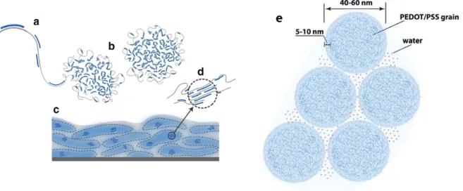
Figure 2.7. Commonly described microstructure of PEDOT:PSS (a) PEDOT synthesis on PSS template, (b) formation of colloidal gel particles in dispersion and (c) resulting film with PEDOT:PSS-rich (blue) and PSS-rich (grey) phases. (d) Aggregates/crystallites support enhanced electronic transport21. (e) The typical diameter of PEDOT/PSS grains is 40–60 nm, with a PSS-rich shell thickness of 5–10 nm36. Reprinted with permission.
2.3.2 Film forming properties
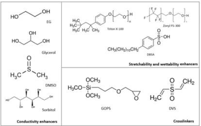
In certain cases, some amphiphilic additives (mostly surfactant), such as DBSA26, Zonyl-FS300 (Zonyl)28 and Triton X-10037 (Figure 2.8), are mixed with the PEDOT:PSS aqueous suspension to improve its film forming ability. For example, Vosgueritchian et al. reported that mixing with the fluorosurfactant Zonyl significantly increases PEDOT:PSS wettability on hydrophobic surfaces due to the amphiphilic nature of the Zonyl, which is composed of both a hydrophobic (fluorinated) and hydrophilic (ethylene glycol) segment. Additives used to increase the PEDOT:PSS wettability usually also increase the film stretchability when the concentration is optimized. For example, we observed the sole addition of DBSA to PEDOT:PSS not only increases film wettability, but also increases the film conductivity, as well as the stretchability. However, adding more than 2% DBSA induces a phase separation in the suspension (similar to the case of adding H2SO4). Further
increases in the DBSA concentration causes a gel-like structure, and makes PEDOT:PSS suspension impossible to be solution processed.
Figure 2.8. Additives used to improve specific properties of PEDOT:PSS.
PEDOT:PSS films easily delaminate from hydrophilic substrates such as glass and silicon, upon water immersion38. Therefore for in-water applications, it is necessary to use a crosslinking agent (such as glycidoxypropyltrimethoxysilane, GOPS) to improve adhesion on substrates and promote long-term resistance to dissolution and delamination, while maintaining effective charge-transport performance26 (Figure 2.8). GOPS is a silane with a polar and reactive epoxide functional group and silanol group after hydrolysis in water. GOPS is compatible with aqueous PEDOT:PSS suspension and can form a network structure after spin-coating. Silanol groups produced from hydrolysis of GOPS react with a surface hydroxyl group on glass or silicon to form siloxane linkage or hydrogen bonding. In addition, GOPS can form a network structure through self-condensation reaction between silanol groups26,39-41. PEDOT:PSS mixed with GOPS is insoluble in any solvent after spin-coating, while pristine PEDOT:PSS is slightly soluble in water. However, GOPS has the disadvantage of decreasing both ionic and electronic mobility in the film42. Recently, it has been reported that divinylsulfone is able to crosslink PEDOT:PSS at room temperature without deteriorating film conductivity43. It looks very promising as a replacement for GOPS (Figure. 2.8).
2.3.3 Flexibility and stretchability
Without doubt, flexibility is a desirable advantage of conducting polymer with respect to Si electronics. Silicon is held together by covalent bonds, where each atom shares valence electrons with four neighbors. In contrast, conducting polymer consists of macromolecular blocks within which atoms are covalently bonded to each other, however these blocks are held together via weak van der Waals or electrostatic interactions. The prevalence of van der Waals interactions in “soft” conducting polymer defines the key difference with the “hard” silicon5. We reported that
PEDOT:PSS on plastic PET can undergo extreme bending of hundreds of cycles with negligible effect on conductivity, indicating excellent intrinsic flexibility of PEDOT:PSS38. We also developed a flexible device on ultrathin parylene films. Moving beyond flexible to more advantageous stretchable forms opens new possibilities for wearable, implantable and conformable electronics. However, the intrinsic stretchability of the pristine PEDOT:PSS is only ~5% which limits its applications30. With this motivation, in 2012, Lipomi et al. optimized the processing condition on PDMS and increased PEDOT:PSS stretchability to 30% by blending with 1% fluorosurfactant Zonyl, without cracks occurring in the film44. They expected that Zonyl would
function as a typical plasticizer in the film by increasing the free soft volume (that can absorb strain) in the film and weakening intermolecular forces between the polymer chains45. In 2015, Li et al. reported that the PEDOT:PSS stretchability can be improved after blending with a series of polymers such as poly(ethylene glycol), poly(ethylene oxide) or poly(vinyl alcohol)46. The stretchability of a thick PEDOT:PSS film was increased from 2% to 55% when blending with poly(vinyl alcohol). They proposed the polymers can mix well with PSS so that they increase soft areas in the polymer matrix46. In 2015, Oh et al. obtained a stretchable dough by blending PEDOT:PSS with the surfactant Triton X-100 to form nanofibril microstructures. They proposed the increased stretchability originated from the formation of softer matrix due to the good miscibility of Triton X-100 with PSS47. In 2017, Wang et al. demonstrated highly stretchable PEDOT:PSS films by incorporating a series of ionic stretchability enhancers such as ionic compounds and ionic liquids (Figure 2.9)30. With these enhancers the conductivity can reach the remarkable value of 4100 S/cm, while remaining above 100 S/cm under 600% strain, with a fracture strain of 800%. They suggested that the stretchability enhancers mix well with PEDOT:PSS and are able to further soften the PSS. Besides, the charge screening effect of the ionic additives leads to more crystalline and more interconnected PEDOT nanofibrillar structures,
thus increasing conductivity. Because the PEDOT phase becomes more crystalline with additives, they suspect the soft additive molecules reside in the more disordered PEDOT regions, which further softens the material, and gives rise to a nanofiber PEDOT network embedded in a soft matrix of the additives, which is a desirable morphology for high stretchability30.
Figure 2.9. Chemical structures and schematic representation. (A) Representative stretchability and electrical conductivity enhancers. (B) Strain-stress curves of PEDOT:PSS with and without stretchability and electrical conductivity (STEC) enhancers. (C and D) Schematic diagram representing the morphology of (C) a typical PEDOT:PSS film versus that of (D) a stretchable PEDOT film with STEC enhancers30. Reprinted with permission.
In addition to increasing the stretchability of PEDOT:PSS thin films, many groups were able to make stretchable PEDOT:PSS gels by blending with elastomer48 or hydrogel49, and stretchable PEDOT fibers by wet spinning50. We recently demonstrated highly stretchable PEDOT:PSS nanofibers via electrospinning. These efforts are paving the way for the development of stretchable interconnects for wearable electronics applications.
2.3.4 Self-healing
Self-healing electronic materials can repair damage caused by frequent bending or external agents. Therefore, they are highly desirable, increasing reliability and longevity of electronic devices51. Although the self-healing abilities of non-conjugated polymer networks have been frequently reported, very few works are dedicated to investigating the self-healing ability of conjugated polymers52. In 2015, Oh et al. reported self-healing of PEDOT:PSS in the form of a dough by blending PEDOT:PSS with 80% (weight ratio) plasticizer Triton X-100. They proposed the reason for the healing is because the capillary shear force from PEDOT:PSS film to the damaged area was larger than the critical shear stress47.
2.4 PEDOT:PSS patterning
Conventional photolithography materials, such as photoresist, developer and strippers, are not suitable for patterning organic electronic materials, because they can dissolve or contaminate the organic semiconductors53,54. Therefore, although simple patterns can be obtained with conventional lithography9,22, alternative strategies need to be found to pattern PEDOT:PSS.
Several alternative methods for patterning organic semiconductors are being investigated. Direct printing technologies such as ink-jet printing, screen printing and roll-to-roll printing can be used for features larger than approximately 10-20 um55,56. While transfer printing and soft lithography using an elastomer stamp increase the resolution, they require critical control of the adhesion between the carrier stamp and donor/acceptor substrates, which sometimes produces low yield due to variation in the contact area57,58. Moreover, lateral collapse of relief structures and sagging of recessed structures of the stamp will result in complete failure of the pattern59.
A decade before, DeFranco et al. introduced thin parylene film (< 2 um) to pattern PEDOT:PSS53. The parylene film can be pre-deposited on glass by chemical vapor deposition and subsequently patterned by conventional photolithography. Deposition of PEDOT:PSS on the patterned parylene layer, followed by a parylene peeling off process, leads to high resolution PEDOT:PSS patterns. The advantage of this method is that the seamless parylene shadow-masking avoids PEDOT:PSS exposure to solvents used in photolithography and thus ensures an unchanged film property after patterning. Since then, parylene patterning has become a widely used method to pattern PEDOT:PSS, especially for the fabrication of OECTs60.
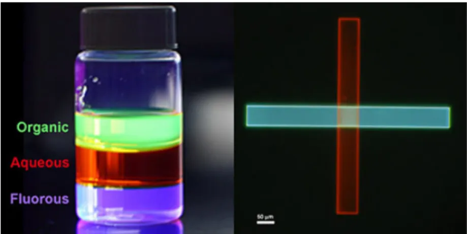
In any case, direct photolithography is one of the most favored technologies for high resolution patterns due to well-established techniques in the industry. Aiming to develop photolithographic materials that are compatible with organic electronic materials, the groups of Malliaras and Ober proposed a new photolithography chemistry based on fluorinated materials, i.e., hydrofluoroethers (HFE)54. HFEs are chemically “orthogonal” to organic compounds, so that organic semiconductors are insoluble and are not swollen in HFEs (Figure 2.10). Thus, this method is named orthogonal photolithography. Despite several demonstrations on rigid substrates61, this technology is still in its early stage. It is, therefore, necessary to investigate its reliability and optimize photolithographic processes on different substrates to facilitate further applications.
Figure 2.10. The immiscibility of fluorous, aqueous, and organic liquids (shown above, left) enables patterning of two overlapping stripes of light-emitting polymers, with the use of a fluorinated photoresist (shown above, right)61. Reprinted with permission.
2.5 The transistor
A transistor is a semiconductor device used to amplify or switch electronic signals and electrical power. Integration of billions of transistors is at the core of industrial electronics, such as processors and memories.62. The invention of the transistor is considered to be one of the most important
inventions of the 20th century. William Shockley, John Bardeen and Walter Brattain were awarded the Nobel Prize in Physics in 1956, “for their researches on semiconductors and their discovery of
2.5.1 Field-effect transistor
The most successful and widely used transistor is the metal-oxide semiconductor field-effect transistor (MOSFET)62. Generally speaking, the most used FETs control current flow in the semiconductor through electrostatic interactions (Figure. 2.11). Two distinct advantages of inorganic (such as silicon) FETs are their excellent stability and fast response speed (up to THz due to high mobility), which permit commercial applications in high frequency communications and high speed data processing. In the past 60 years, inorganic FETs have garnered extraordinary success in industry because of advances in the development of semiconductor materials and well-established manufacturing processes. We have witnessed the rapid development of inorganic FETs. From the initial 10 um process developed by Intel in 1971, to the 14 nm process in 2014, and then to the 10 nm process in 201763, FETs have dominated the development of the electronics industry.
2.5.2 Electrochemical transistor
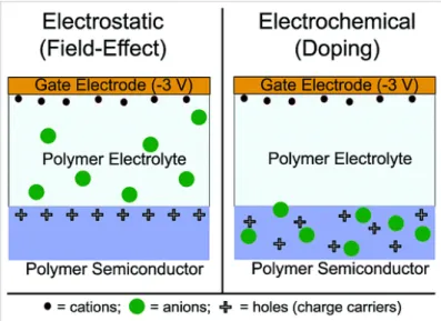
An electrochemical transistor (ECT) uses electrolyte as the gating medium7. When a gate bias is applied to the electrolyte, ions migrate into the semiconductor and trigger an electrochemical reaction, or doping/dedoping process (Figure. 2.11), which modulates film conductivity7. Metal oxides and conducting polymers are well-known candidates for channel materials in electrochemical transistors.
Figure 2.11. Cross-sections of polymer EG transistors showing the difference between (a) electrostatic FET and (b) electrochemical doping ECT7. Reprinted with permission.