HAL Id: hal-01736115
https://hal.archives-ouvertes.fr/hal-01736115
Submitted on 22 Mar 2018
HAL is a multi-disciplinary open access
archive for the deposit and dissemination of
sci-entific research documents, whether they are
pub-lished or not. The documents may come from
teaching and research institutions in France or
abroad, or from public or private research centers.
L’archive ouverte pluridisciplinaire HAL, est
destinée au dépôt et à la diffusion de documents
scientifiques de niveau recherche, publiés ou non,
émanant des établissements d’enseignement et de
recherche français ou étrangers, des laboratoires
publics ou privés.
Clusters formation in ultralow-energy high-dose
boron-implanted silicon
Fuccio Cristiano, Xavier Hebras, Nikolay Cherkashin, Alain Claverie, W.
Lerch, S. Paul
To cite this version:
Fuccio Cristiano, Xavier Hebras, Nikolay Cherkashin, Alain Claverie, W. Lerch, et al.. Clusters
formation in ultralow-energy high-dose boron-implanted silicon. Applied Physics Letters, American
Institute of Physics, 2003, 83 (26), pp.5407-5409. �10.1063/1.1637440�. �hal-01736115�
Clusters formation in ultralow-energy high-dose boron-implanted silicon
F. Cristiano, X. Hebras, N. Cherkashin, A. Claverie, W. Lerch, and S. Paul
Citation: Appl. Phys. Lett. 83, 5407 (2003); doi: 10.1063/1.1637440 View online: https://doi.org/10.1063/1.1637440
View Table of Contents: http://aip.scitation.org/toc/apl/83/26 Published by the American Institute of Physics
Articles you may be interested in Transient enhanced diffusion of boron in Si
Journal of Applied Physics 91, 8919 (2002); 10.1063/1.1471941
Rapid annealing and the anomalous diffusion of ion implanted boron into silicon Applied Physics Letters 50, 416 (1987); 10.1063/1.98160
Trap-limited interstitial diffusion and enhanced boron clustering in silicon Applied Physics Letters 66, 568 (1995); 10.1063/1.114015
{311} defects in silicon: The source of the loops
Applied Physics Letters 73, 3748 (1998); 10.1063/1.122882 Diffusion of boron in silicon during post-implantation annealing Journal of Applied Physics 69, 2135 (1991); 10.1063/1.348740
Transient boron diffusion in ion-implanted crystalline and amorphous silicon Journal of Applied Physics 63, 1452 (1988); 10.1063/1.339926
Clusters formation in ultralow-energy high-dose boron-implanted silicon
F. Cristiano,a)X. Hebras, N. Cherkashin, and A. Claverie
Ion Implantation Group CEMES/LAAS-CNRS, 7 av. du Col. Roche, 31077 Toulouse, France
W. Lerch and S. Paul
Mattson Thermal Products GmbH, Daimlerstrasse 10, D-89160 Dornstadt, Germany 共Received 16 September 2003; accepted 7 November 2003兲
The formation and evolution of small cluster defects in 500 eV, 1⫻1015 cm⫺2 boron-implanted silicon is investigated. These clusters are identified by high-resolution transmission electron microscopy共TEM兲 as small dislocation loops lying on 兵100其 planes with an interstitial character. Weak-beam dark-field TEM analysis shows that, during annealing at 650 °C, they evolve following an Ostwald ripening mechanism. Spike anneals at high temperatures make them dissolve but an immobile boron peak is still detected in the secondary ion mass spectroscopy profiles. Upon oxidation, the average size of the clusters increases, while boron electrical deactivation occurs. These results strongly indicate that the observed clusters contain both boron interstitials and silicon self-interstitials atoms. © 2003 American Institute of Physics. 关DOI: 10.1063/1.1637440兴
To continue scaling down complementary metal–oxide– semiconductor devices, ultrashallow and extremely highly doped p⫹/n junctions must be fabricated.1 As a conse-quence, boron is implanted at doses that exceed its equilib-rium solid solubility limit in silicon. During annealing the boron peak region is therefore found to be immobile and electrical inactive. This is a major roadblock for meeting the ITRS specifications of low sheet resistance in the layers. Pre-vious studies have invoked the formation of either a silicon boride phase (SiB4
2,3
or SiB3) 4
or Si–B clusters 共BICs兲 made of very few atoms5,6to explain this behavior. However, while very few studies have investigated the formation of boron precipitates above the solid solubility limit,3,7,8the for-mation of BICs has been mostly investigated at lower B concentrations.9,10 No transmission electron microscopy
共TEM兲 evidence for BICs has been given so far, this being
interpreted as BICs being very small objects involving only very few atoms.6This description is supported by theoretical studies of the formation of BICs, which also assume that a very limited number of Si and B atoms are contained in the clusters.5
In this letter, we present an experimental study of samples implanted in typical conditions for the formation of ultrashallow and extremely highly doped p⫹/n junctions. By using specific TEM imaging conditions it has been possible to establish the structure and to observe the evolution of small clusters formed during annealing in the implanted lay-ers. These clusters definitely differ from already reported pure Si interstitial defects and probably result from the co-precipitation of B and Si. We will show that, despite the very high B concentration levels (⬃1021cm⫺3), no precipitation of a boride phase is achieved in these structures and that, despite being much larger than ‘‘conventional’’ BICs, the observed clusters exhibit an annealing behavior typical of small boron-interstitial clusters.
Chemically etched 共100兲 Si wafers of 8–20 ⍀ cm were
implanted with 500 eV boron ions to a dose of 1
⫻1015 ions/cm2 using a Varian VIIta-80 ULE high current
implanter and annealed on a Mattson 2900 or 3000 rapid thermal annealing共RTA兲 system at 650 and 750 °C for times ranging from 2 to 160 s in flowing N2or O2. Subsequent to a 650 °C 10 s N2 anneal 共pre stabilization step兲, selected samples were spike annealed at 1050 and 1100 °C using a 250 °C/s ramp-up rate. Boron concentration profiles have been measured by secondary ion mass spectroscopy共SIMS兲, while electrical activation has been assessed by sheet resis-tance and spreading resisresis-tance profiling 共SRP兲 measure-ments. TEM analysis was performed on a JEOL 2010-HC system using weak-beam dark-field共WBDF兲 imaging condi-tions using a 共220兲 diffracting vector, g. Selected samples were observed in high-resolution electron microscopy
共HREM兲 conditions using a Philips CM30 microscope.
Figure 1 shows typical SIMS profiles obtained before and after annealing at several temperatures in a N2 ambient.
Although not evident from the as-implanted curve, all SIMS profiles taken after annealing show that the boron concentra-tion peak is located at a depth of about 2 nm, in agreement with the expected value for an implantation energy of 500 eV, while the boron peak concentration level clearly exceeds its solubility limit in silicon at all temperatures considered in
a兲Author to whom correspondence should be addressed; electronic mail:
FIG. 1. B⫹ SIMS profiles after implantation at 500 eV to a dose of 1 ⫻1015cm⫺2. Circles: as-implanted. Solid line: annealed at 650 °C for 10 s. Dashed line: annealed at 650 °C for 10 s⫹spike anneal at 1050 °C. Dotted line: annealed at 650 °C for 10 s⫹spike anneal at 1100 °C.
APPLIED PHYSICS LETTERS VOLUME 83, NUMBER 26 29 DECEMBER 2003
5407
this study共about 1.5⫻1019, 1.5⫻1020, and 2⫻1020cm⫺3at 650, 1050, and 1100 °C, respectively兲.7 Boron is therefore expected to easily precipitate. Unfortunately, after a low ther-mal budget anneal共650 °C 10 s, solid line in Fig. 1兲, it is not possible from the SIMS data to distinguish any immobile part of the profile 共in the peak region兲 from the mobile one
共diffusive tail兲. However, SRP measurements from samples
annealed at 650 °C共not shown兲 indicate that, independently of the annealing time, the maximum boron activation level never exceeds 2⫻1019 cm⫺3, suggesting that boron cluster-ing actually occurs at this temperature. SRP measurements taken after spike anneals at 1050 and 1100 °C show an in-crease in the electrical activation level, with sheet resistance values decreasing from 12 000 ⍀/䊐 at 650 °C down to 390 and 260 ⍀/䊐 at 1050 and 1100 °C, respectively. Neverthe-less, it is found again that the maximum dopant activation does not exceed the solid solubility concentration level. This is confirmed by the SIMS profiles共dashed and dotted lines in Fig. 1, respectively兲, both exhibiting an immobile peak at high concentration levels共above ⬃2⫻1020 cm⫺3) and a dif-fusive tail at lower concentrations. It is important to note that, although boron clustering is detected at all annealing temperatures, the maximum concentration level of the immo-bile peak decreases from 2⫻1021cm⫺3 at 650 °C to 5
⫻1020cm⫺3 at 1100 °C, indicating that the clusters formed
during annealing are unstable with respect to the annealing temperature and tend to dissolve.
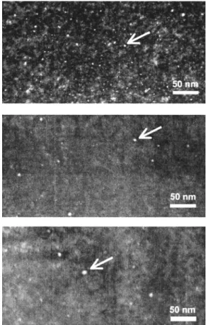
Figure 2共a兲 shows a typical WBDF plan-view image 共g, 5g兲 of a sample annealed at 650 °C. Under these imaging conditions, small clusters appear as white circular dots on a dark background 共indicated by arrows in the figure兲, with diameters ranging from 1 to about 10 nm. HREM analysis in cross-section samples 关Fig. 2共b兲兴 shows that the observed defects are located at a depth of about 2.5 nm below the surface, corresponding to the location of the peak of the bo-ron concentration profile 共see Fig. 1兲. These defects have been observed in all samples annealed at low temperature
共650 and 750 °C兲 independently of the annealing time and
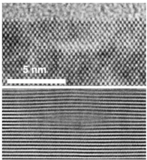
atmosphere (N2 or O2). In contrast, no defects were detected after high temperature spike anneals at 1050 and 1100 °C. Figure 3共a兲 is an enlarged image of one defect, while Fig. 3共b兲 is obtained after Fourier filtering of the experimental image. Such image treatment allows us to identify these de-fects as being small dislocation loops lying on 兵100其 planes
and exhibiting an interstitial character关see the extra plane in Fig. 3共b兲兴. This structure is consistent with the contrast ob-served under WBDF conditions on plan-view samples. Pre-vious investigations of low-energy high dose boron im-planted silicon did not report the presence of any kind of defects after annealing.11 There are two main reasons for that. The first one is that much higher temperature annealing is often used and the 兵100其 defects reported here probably dissolve during the ramp-up. The second reason is that these defects are not visible by TEM unless far-from-Bragg WBDF conditions are used, which is the only way to resolve the weak strain field surrounding these extremely small de-fects. On the other hand, the presence of ‘‘rod-like’’ defects lying on兵100其 planes had already been reported in the 1970s following higher energy B⫹ implants 共40 keV12 and 100 keV兲.13 However, the habit plane of these defects was de-duced on the basis of contrast extinction criteria without any evidence based on HREM. The difficulty in determining un-ambiguously the habit planes of these defects, due to their narrowness, suggests that the reported defects were instead the共today兲 well-known 兵113其 defects.14The first HREM evi-dence of兵100其 loops in Si was finally given a few years later in electron irradiated Si.15 In order to investigate in more detail the nature of these clusters, we have studied by WBDF TEM their evolution upon annealing at 650 °C. Figure 4 shows WBDF TEM micrographs关共a兲–共c兲兴 from samples an-nealed for 2, 10, and 160 s, respectively. Despite the diffi-culty in extracting quantitative information from WBDF im-ages of small clusters, due to the strong dependence of the clusters image size on the imaging conditions,16these images clearly show that the average cluster size 共of about 2 nm after 2 s annealing兲 increases by about a factor 3 after 160 s, while their density decreases by one decade. This behavior is typical of an Ostwald ripening mechanism for the defect growth,17 where large clusters grow at the expense of the small ones by interchanging the atoms they are composed of. Additional experiments 共not shown兲 suggest that the injec-tion of Si atoms due to a slight oxidainjec-tion of the surface results in the growth of these defects. The electrical
activa-FIG. 2.共a兲 Typical weak-beam plan-view TEM image of a sample annealed at 650 °C.共b兲 HREM cross-sectional image showing defects position at 2.5 nm below the surface.
FIG. 3. 共a兲 Original HREM image of a defect. 共b兲 Fourier filtered image obtained using兵200其 diffracted spots.
tion is also found to decrease during oxidation, in agreement with similar recent experiments.18
SIMS measurements共Fig. 1兲 have shown that boron ex-ceeds its solubility limit for the experimental conditions used in this study and can therefore easily precipitate. Indeed, the fact that the defects are formed at the same depth as the peak of boron concentration, in conjunction with the observation of an immobile B peak even after high temperature anneal-ing, clearly indicates that these defects must contain boron atoms. However, the maximum concentration level of the immobile peak progressively decreases when increasing the annealing temperature, indicating that the clusters tend to dissolve, i.e., they are not the precursors of a stable second phase, typical of a precipitation process above solid solubil-ity. In such cases, precipitates are observed well above 1000 °C.3,7,8In addition, although they are still detected by SIMS at high temperature, they are no longer seen by TEM, indicating that their size probably decreases below the TEM detection limit. The observed growth of the兵100其 loops dur-ing oxidation 共Si interstitials injection conditions兲 suggests that these defects probably contain Si atoms. However, they cannot be pure Si interstitials defects, as, although small, pure Si defects of the observed dimensions would contain hundreds of atoms and rearrange in more energetically
favor-able forms关兵113其s or 共111兲 dislocation loops兴, easily detect-able by TEM.17 In addition, calculations of the strain field surrounding the defects19,20 show that, should the defects consist of Si atoms only, each of them would be able to trap less than one B atom at its periphery. The observed defect density共of the order of 1012cm⫺2) cannot therefore account for the amount of immobile boron atoms estimated by SIMS
共no less than 1014cm⫺2), i.e., boron atoms must be
con-tained in the core of the defects. The most probable explana-tion of the results obtained in this work is therefore that the
兵100其 defects are B–Si interstitial complexes, i.e., BICs of
hundreds of atoms. This might be the evidence that BICs can be imaged by TEM and thus can be much bigger than gen-erally assumed.
In summary, we have studied the structure and thermal evolution of small two-dimensional兵100其 clusters found af-ter RTA annealing of ultralow energy high-dose B⫹ im-planted Si. During annealing at low temperature, these de-fects evolve following an Ostwald ripening mechanism. Spike anneals at high temperatures make them dissolve but a secondary peak of boron remains in the profile. Both Si and B atoms are contained in the defects. These results indicate that boron interstitial clusters can be imaged by TEM and thus can be much bigger than generally assumed.
This work is part of the FRENDTECH Project and funded by the EC as IST/2000-30129.
1E. C. Jones and E. Ishida, Mater. Sci. Eng., R. 24, 1共1998兲. 2S. Solmi, E. Landi, and F. Baruffaldi, J. Appl. Phys. 68, 3250共1990兲. 3
A. Agarwal, H. J. Gossman, D. J. Eaglesham, L. Pelaz, S. B. Herner, D. C. Jacobson, T. E. Haynes, and R. Simonton, Mater. Sci. Semicond. Process.
1, 17共1998兲.
4N. E. B. Cowern, M. J. J. Theunissen, F. Roozeboom, and J. G. M. van
Berkum, Appl. Phys. Lett. 75, 181共1999兲.
5
L. Pelaz, G. H. Gilmer, H.-J. Gossmann, C. S. Rafferty, M. Jaraiz, and J. Barbolla, Appl. Phys. Lett. 74, 3657共1999兲.
6P. Pichler, Mater. Res. Soc. Symp. Proc. 717, 103共2002兲.
7A. Armgliato, D. Nobili, P. Ostoja, M. Servidori, and S. Solmi, in
Elec-trochem. Soc. Proc. 77-2: Semiconductor Silicon 1977, edited by H. R. Huff and E. Sirtl,共1977兲, p. 638.
8T. L. Aselage, J. Mater. Res. 13, 1786共1998兲.
9N. E. B. Cowern, K. T. F. Janssen, and H. F. F. Jos, J. Appl. Phys. 68, 6191
共1990兲.
10
S. Solmi, F. Baruffaldi, and R. Canteri, J. Appl. Phys. 69, 2135共1991兲.
11L. H. Zhang, K. S. Jones, P. H. Chi, and D. S. Simons, Appl. Phys. Lett. 67, 2025共1995兲.
12P. K. Madden and S. M. Davidson, Radiat. Eff. 14, 271共1972兲. 13
W. K. Wu and J. Washburn, Cryst. Lattice Defects 7, 39共1977兲.
14J. A. Lambert and P. S. Dobson, Philos. Mag. 44, 1043共1981兲. 15M. Pasemann, D. Hoehl, A. L. Aseev, and O. P. Pchelyakov, Phys. Status
Solidi 80, 135共1983兲.
16M. L. Jenkins, M. A. Kirk, and H. Fukushima, J. Electron Microsc. 48,
323共1999兲.
17A. Claverie, B. Colombeau, B. De Mauduit, C. Bonafos, X. Hebras, G. B.
Assayag, and F. Cristiano, Appl. Phys. A: Mater. Sci. Process. 76, 1025 共2003兲.
18
L. Radic, A. D. Lilak, and M. E. Law, Appl. Phys. Lett. 81, 826共2002兲.
19
J. P. Hirth and J. Lothe, Theory of Dislocations,共McGraw-Hill, New York, 1968兲, pp. 462–465.
20J. F. Gibbons, Radiat. Eff. 6, 313共1970兲.
FIG. 4. TEM micrographs from samples annealed at 650 °C for 2, 10, and 160 s, respectively.
5409