Délivré par l’Université Toulouse 3–Paul Sabatier
Présentée et soutenue par
Sovannarith LENG
le 20 Février 2017
Identifying and Evaluating Aging Signatures in Light Emitting Diode Lighting Systems
École doctorale et discipline ou spécialité
ED GEET : Génie Electrique
Unité de recherche
Laboratoire PLAsma et Conversion d’Energie (LAPLACE)
Directeurs de Thèse
Dr. Laurent CANALE, CNRS, LAPLACE
Prof. Georges ZISSIS, Université Paul Sabatier, LAPLACE
Jury
Christian GLAIZE, Professeur, Lab. IES, Groupe GEM, Montpellier, Rapporteur Yannick DESHAYES, Dr/HDR, IMS, Groupe ONDE, EDMINA, Talence, Rapporteur Geneviève DUCHAMP, Professeur, IMS, Groupe FIABILITE, Bordeaux, Examinateur
Laurent MASSOL, Ingénieur, Directeur Société LED, Montauban, Invité Laurent CANALE, Dr, Ingénieur de Recherche CNRS, LAPLACE, Directeur de Thèse
Laboratoire LAPLACE
THÈSEPour obtenir le grade de DOCTEUR DE L’UNIVERSITÉ
Spécialité
Identifying and Evaluating Aging
Signatures in Light Emitting Diode
Lighting Systems
Sovannarith LENG
Présentée et soutenue publiquement Le 20 Février 2017
Directeurs
Dr. Laurent CANALE, Ingénieur de Recherche CNRS, LAPLACE Prof. Georges ZISSIS, Université Paul Sabatier, LAPLACE
JURY
Christian GLAIZE, Professeur, Lab. IES, Groupe GEM, Montpellier, Rapporteur Yannick DESHAYES, Dr/HDR, IMS, Groupe ONDE, EDMINA, Talence, Rapporteur Geneviève DUCHAMP, Professeur, IMS, Groupe FIABILITE, Bordeaux, Examinateur
Laurent MASSOL, Ingénieur, Directeur Société LED, Montauban, Invité Laurent CANALE, Dr, Ingénieur de Recherche CNRS, LAPLACE, Directeur de Thèse
A
ACKNOWLEDGEMENTS
This thesis was carried out within the PLAsma and Conversion d'Energie (LAPLACE) laboratory in Toulouse. This exciting and rewarding research has led to the contribution of several staff from the laboratory. I would therefore like to express my gratitude to certain individuals who have devoted their efforts and their availabilities to me during this thesis.
First of all, I would like to express my deep gratitude to my supervisor, Georges ZISSIS, Professor at University Paul Sabatier in Toulouse, Head of Light & Matter Research Group at LAPLACE and Director of SH2D Research Federation, for his very important direction in my work and for his encouragement, his advice and his very valuable technical and moral support for the success of my work.
I would also like to express my sincere thanks to my co–supervisor, Dr. Laurent CANALE, CNRS Research Engineer in Light & Matter Research Group and AFE Midi–Pyrénées Region Chairman, for his encouragement, his guidance, including his very useful advice which enabled me to acquire knowledge and skills that are very useful for my research and my career.
I especially wish to thank my thesis committee: Professor Christian GLAIZE, at "Institut d'Electronique et des Systèmes" in Montpellier, Professor Geneviève DUCHAMP, and Dr Yannick DESHAYES, Associate Professor/HDR, both from University of Bordeaux and "Laboratoire de l'Intégration du Matériau au Système", for their valuable advices, thesis supervision, and their positive comment and evaluation on my thesis.
I do not forget to express my gratitude to all staffs, lecturers, professors, PhD students and colleagues of the Laplace with whom I shared very pleasant moments and which allowed me to acquire various technical, social and cultural
knowledges on countless occasions. I would like to specially thank to my best friends, Alaa ALCHADDOUD and Feng TIAN.
I also do not forget to convey my thanks to my Cambodian friends who are / were in Toulouse and France, with whom I shared a lot of pleasant moments and who remain anchored in my memories.
Very special and from bottom of heart thanks and gratitude to my beloved family: mmy wife, my son and my parent for their love, constant moral encouragement, and their invaluable sacrifice of everything for me. They always support and hold me when I am down so I never lost my spirit. No word I can say about their goodness. I am very proud to be their part of family. I also thank to my brothers and sisters for caring and support. It is to all of them that I dedicate this thesis.
The last but not least, I would like to express my deepest appreciation to Erasmus Mundus Techno II project with the support of the Erasmus Mundus Program of the European Union for my financial support, to officers and staffs of the Techno II program for their kindness and help during my study.
Contents
INTRODUCTION ... 1
1. STATE OF THE ART OF THE GaN LEDS TECHNOLOGY ... 5
1.1.HISTORY OF LIGHTING SYSTEMS ... 6
1.1.1. The Sun ... 6
1.1.2. Incandescent Filament Lamp ... 7
1.1.3. Mercury and Sodium Vapor Lamps ... 7
1.1.4. Fluorescent Lamp ... 9
1.1.5. Light–Emitting Diodes (LEDs) ... 10
1.2.LED CHIP STRUCTURES ... 14
1.2.1. Conventional Lateral and Vertical Structure ... 14
1.2.2. Flip Chip Structure ... 15
1.2.3. Vertical Thin Film Structure ... 16
1.2.4. Thin Film Flip Chip Structure ... 17
1.3.PACKAGING OF LEDS ... 18
1.3.1. Low Power LED Package ... 19
1.3.2. High Power LED Package ... 19
1.3.3. Packaging Process ... 21
1.3.3.1. Dual in–Line (DIP) Packaging ... 22
1.3.3.2. SMD LED Packaging ... 22
1.3.3.2.1. SMD Leadform Packaging ... 23
1.3.3.2.2. SMD Leadless Package ... 24
1.3.3.3. LED Array Packaging ... 26
1.4.MAIN DEGRADATION OF LEDS TECHNOLOGY... 29
1.4.1. Degradation and Failure Modes at Chip Level ... 29
1.4.1.1. Generation and Movement of Defect and Dislocation ... 29
1.4.1.2. Die Cracking ... 32
1.4.1.3. Dopant Diffusion ... 34
1.4.1.4. Electromigration ... 34
1.4.2. Interconnection Failure Modes ... 35
1.4.2.1. Bond Wire /Wire Ball Bond Failure ... 35
1.4.2.2. Electrical Contact Metallurgical Interdiffusion... 37
1.4.2.3. Electrostatic Discharge ... 37
1.4.3. Degradation and Failure Modes at Package Level ... 40
1.4.3.1. Carbonization of the Encapsulant ... 40
1.4.3.2. Delamination ... 41
1.4.3.3. Lens /Encapsulant Failure ... 43
1.4.3.5. Solder Joint Fatigue ... 46
1.5.CONCLUSION –CHAPTER 1 ... 47
2. ELECTRICAL AND OPTICAL CHARACTERISTICS OF LEDS ... 51
2.1.METHODOLOGY FOR JUNCTION TEMPERATURE EVALUATION ... 52
2.1.1. Temperature Dependence of Forward Voltage (Vf) ... 53
2.2.OPTICALPROPERTIESOFLED ... 60
2.2.1. Internal, Extraction, External, and Power Efficiencies ... 60
2.2.2. Emission Spectrum ... 61
2.2.3. Light Escape Cone ... 64
2.2.4. Radiation Pattern–Lambertian Emission Pattern ... 66
2.2.5. Epoxy Encapsulant ... 67
2.2.6. Temperature Dependence of Emission Intensity ... 68
3. EXPERIMENTAL SETUP FOR LED AGING EVALUATION ... 69
3.1.ANEWPROTOTYPEOFLEDAGINGBENCH ... 70
3.2.TEMPERATURE CONTROLLER (REX–D100) ... 76
3.2.1. Software Program for REX–D100 Temperature Controller ... 78
3.2.2. Communication Protocol ... 80
3.2.2.1. Polling Procedure ... 80
3.2.2.1. Selection Procedure ... 81
3.3.SOURCE–METER UNIT (SMU–KEITHLEY 2602A) ... 81
3.3.1. 2–Wires and 4–Wires Feature ... 82
3.3.2. Software Program Measurement for SMU–Keithley 2602A ... 83
3.4.IMPEDANCE ANALYZER (SOLARTRON MODULAB) ... 87
3.4.1. Instrument Group Modules ... 87
3.4.2. PC Communication Setup ... 88
3.4.3. Software Program Control of Solartron ModuLab ... 89
3.5.SPECTROMETER (SPECBOS 1201) ... 91
3.5.1. Optical Measurement Hardware Setup ... 92
3.5.2. Software Program Measurement of Specbos 1201 ... 93
3.6.LED’S DRIVER ... 94
4. EVALUATION OF FAILURE MECHANISMS FOR LEDS STUDIED ... 97
4.1.EFFECT OF TEMPERATURE ON LEDPERFORMANCE... 98
4.2.SELF−HEATING TEST... 100
4.3.INITIAL STATE OF ELECTRICAL CHARACTERIZATIONS... 101
4.4.1. Electrical Aging Characteristic of Cree’s Devices... 111
4.4.2. Electrical Aging Characteristic of Osram’s Devices ... 115
4.4.3. Electrical Aging Characteristic of Philips’s Devices ... 118
4.4.4. Electrical Aging Characteristic of Seoul’s Devices ... 122
4.5.OPTICAL FAILURE SIGNATURES ... 126
4.5.1. Initial State of Photometric Characterization ... 127
4.5.2. Photometrical Characterizations of LEDs under accelerated aging conditions ... 136
4.6.CONCLUSION–CHAPTER 4 ... 146
GENERAL CONCLUSION AND PERSPECTIVES ... 149
REFERENCES... 155
ANNEXES ...I APPENDIX A:COMMUNICATION IDENTIFIER LIST OF REX–D100 ... II
APPENDIX B:CONTROLLER SCANNED PARAMETER ... IV
APPENDIX C:PROGRAM CODE FOR REX–D100 ... V
APPENDIX D:PROGRAM CODE FOR SMUKEITHLEY 2602A ... XI
...
Liste des tableaux
Table I.1: Discoveries and History of LEDs ... 13
Table I.2: Comparison of Key Characteristics and Parameter Values for Commercial ... 14
Table I.3: Factors influent LED packaging ... 21
Table II.1: Varshni parameters of common semiconductors. ... 57
Table III.1: Main characteristics of studied LEDs. ... 71
Table IV.1: dispersion of I−V characteristic of 16 Samples each LED group computed at V=2.9V. ... 104
Table IV.2: Error of variation of luminance and spectrum of 16 samples each unstressed LED group @350mA. ... 131
Table des illustrations Figure I.1: Sun, the first light source. ... 6
Figure I.2: Artificial Lighting. ... 6
Figure I.3: Mercury Vapor Lamp. ... 7
Figure I.4: Low–pressure sodium vapor lamp... 8
Figure I.5: High–pressure sodium vapor lamp. ... 9
Figure I.6: Fluorescent lamp. ... 10
Figure I.7: Publication of JH Round in Electrical World. ... 11
Figure I.8: A replication of H. J. Round's LED experiments. ... 11
Figure I.9: a) Lateral structure, b) vertical structure. ... 15
Figure I.10: Flip chip structure. ... 16
Figure I.11: LED ThinGaN structure by Osram. ... 16
Figure I.12: TFFC by Philips Lumiled. ... 17
Figure I.13: SEM images of PSS and GaN grown on PSS . ... 17
Figure I.14: SEM of an N–face GaN surface roughening etched by a KOH–based PEC method . ... 18
Figure I.15: Al–oxide honeycomb nanostructure on thin–GaN LED . ... 18
Figure I.16: a) LED with hemispherical encapsulant, b) LEDs with cylindrical and rectangular encapsulant . ... 19
Figure I.17: High power LED packaging. ... 20
Figure I.18: Typical package products of high power LED. ... 20
Figure I.19: Packaging process flows of common LEDs . ... 21
Figure I.20: DIP Packaging . ... 22
Figure I.21: a) Leadform package, b) leadless package. ... 23
Figure I.22: Main components of the SMT LED package . ... 23
Figure I.23: Packaging of lateral LED chip. ... 24
Figure I.24: Packaging of vertical LED chip. ... 24
Figure I.25: Packaging of flipped chip LED structure. ... 24
Figure I.26: SMD leadless LED packaging. ... 25
Figure I.27: Leadless Wicop2 module (Chip-on-board packaging, Seoul Semiconductor) . ... 25
Figure I.28: QFN LED package (Oslon Black Flat, Osram) . ... 26
Figure I.29: Multichip LED package . ... 26
Figure I.30: Comparison of Rth for each LED chip in 1–, 4–, and 16–chip packages . ... 27
Figure I.31: COB LED package of some leading products. ... 28
Figure I.32: Dislocations in GaN and discontinuations in Au–metallization . .... 30
Figure I.33: (a) An AFM image and (b) a cross–section TEM image of a pit . ... 30
Figure I.34: Dark–spot defects generation (a), (b), and (c) correspond to initial stage and aging of 67 and 310 h, respectively . ... 31
Figure I.35: a) Good die with proper bonding, b) cracking die with over pressure boding . ... 32
Figure I.36: Large edge defect caused by dicing . ... 32
Figure I.37: Die surface morphology (a) polished, (b) ground, and (c) untreated.33 Figure I.38: Thermal expansion coefficients of GaN/Si and GaN/Sapphire. ... 33
Figure I.39: Maximum EL output power as a function of the integrated Mg concentration . ... 34
Figure I.40: Optical microscope photograph of electrode surface before stress and after device failure . ... 35
Figure I.41: Banding pad divorced from banding area . ... 35
Figure I.42: Breaking of wire neck or heat affected zone (HAZ) . ... 36
Figure I.43: Crack in electrode bonding interface . ... 36
Figure I.44: TEM of MHEMT with Pt/Ti/Pt/Au gate before and after stress ... 37
Figure I.45: Si submount as Zener diode for ESD protection in flip chip structure . ... 38
Figure I.46: GaN LED with an internal Schottky diode and its equivalent circuit model . ... 39 Figure I.47: (a) Bare–chip of LED, (b) Equivalent circuit, (c) an inverse–parallel– connected GaN ESD diode and (d) a GaN LED . ... 39 Figure I.48: Carbonization of phosphor–encapsulating material . ... 40 Figure I.49: a) Optical power b) Output spectra, degradation during stress at 200°C . ... 41 Figure I.50: Possible delamination areas of LEDs. ... 41 Figure I.51: Delamination between the LED die and encapsulant . ... 42 Figure I.52: SEM photographs of the cross–section of degraded (a) Au80Sn20
eutectic sample and (b) silver paste sample . ... 42 Figure I.53: (a) Delamination and (b) curling of phosphor coated LED package . ... 43 Figure I.54: Encapsulant yellowing . ... 43 Figure I.55: Relative light output from 5–mm indicator lamps and high–power illuminator LEDs . ... 44 Figure I.56: Degradation of phosphor (left: untreated sample, right: after stress at 100 A.cm−2, 120°C) . ... 45 Figure I.57: Lifetime result of LED with (a) remote and (b) die–contact phosphor . ... 45 Figure I.58: Creep strain rate vs. tensile stress for different SACxx alloys . ... 46 Figure I.59: Solder fracture due to creep–fatigue under thermal cyclic load . .... 46 Figure I.60: Solder joint cracks (left: SAC305, right: Innolot) ... 47 Figure II.1: Energy loss of carriers as they are captured into the quantum well. ... 53 Figure II.2: Current–voltage characteristic of LED showing threshold voltages 2.0 and 1.6 V, at 77°K and 300°K, respectively... 58 Figure II.3: (a) Pulsed calibration and (b) determination of junction temperature for different DC forward currents. ... 58 Figure II.4: (a) Pulsed calibration measurement (small duty cycle 0.1 %) and (b) junction temperature (Tj) versus DC current of AlGaN UV LED, Schubert, 2006
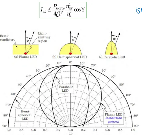
[17, p. 109]. ... 59 Figure II.5: Parabolic electron and hole dispersion relations. ... 61 Figure II.6: Theoretical emission spectrum of an LED. ... 63 Figure II.7: (a) Definition of the escape cone by the critical angle c. (b) area
element dA. (c) area of calotte–shaped section of sphere defined by radius r and angle c. ... 64
Figure II.8: Light–emitting diodes with (a) planar, (b) hemispherical, and (c)
parabolic surfaces, (d) Far–field patterns of the different types of LEDs. ... 66
Figure II.9: (a) LED without, (b) with dome–shaped epoxy encapsulant, (c) calculated ratio of light extraction efficiency emitted through the top surface of a planar LED with and without an epoxy dome... 67
Figure III.1: Overview of the LED aging Bench. ... 70
Figure III.2: Overall experimental setup design. ... 71
Figure III.3: Led types: a) Cree, XLamp® XP–G2 b) Osram, LCW CQ7P.CC c) Philips, LX18–P130–3 and d) Seoul, N42180H–T2. ... 72
Figure III.4: LEDs mounted on a printed custom–made circuit board. ... 72
Figure III.5: LED aluminum holder. ... 73
Figure III.6: stainless steel flexible hose fitting. ... 74
Figure III.7: Arrangement of the stress condition. ... 75
Figure III.8: Temperature controller REX–D100. ... 76
Figure III.9: Control mode of REX–D100. ... 77
Figure III.10: Electrical wiring of experimental setup. ... 78
Figure III.11: Application program for REX–D100 controller. ... 80
Figure III.12: Two–wires connections. ... 82
Figure III.13: Four–wires connections. ... 83
Figure III.14: Application program for SMU–Kethley 2602A. ... 85
Figure III.15: Sweep modes a) linear, b) logarithmic and c) list. ... 86
Figure III.16: LED measurement configuration. ... 88
Figure III.17: Networking to PC. ... 89
Figure III.18: Software control of ModuLab. ... 89
Figure III.19: C–V Characteristic measurement... 90
Figure III.20: Impedance measurement. ... 90
Figure III.21: Fitting and equivalent circuit of a measured sample. ... 91
Figure III.22: Setup measured distance. ... 92
Figure III.23: Photometrical measurement setup. ... 93
Figure III.24: Jeti Lival program for Specbos 1201 control and measure. ... 93
Figure III.25: Drivers of LED samples. ... 94
Figure III.26: Current regulator circuit. ... 95
Figure IV.1: Temperature effect on LED, linear scale. ... 99
Figure IV.2: Temperature effect on LED, semi–log scale. ... 99
Figure IV.3: Linearity of forward voltage to temperature. ... 100
Figure IV.4: Source mode (a) Linear pulse, (b) Linear DC sweep. ... 101
Figure IV.5: I−V Curve, self–heating test. ... 101
Figure IV.6: I−V characteristic of Cree@350mA, linear. ... 102
Figure IV.7: I−V characteristic of Cree@350mA, semi–log. ... 103
Figure IV.8: I−V characteristic of Cree@1000mA, linear. ... 103
Figure IV.9: I−V characteristic of Cree@1000mA, semi–log. ... 103
Figure IV.10: Error bar around average value of 16 samples Cree@350mA, semi– log. ... 104
Figure IV.11: Error bar around average value of 16 samples Cree@1000mA, semi–log. ... 105
Figure IV.12: Error bar around average value of 16 samples Cree@350mA, linear. ... 105
Figure IV.13: Error bar around average value of 16 samples Cree@1000mA, linear. ... 106
Figure IV.14: I−V characteristic of Philips, linear. ... 108
Figure IV.15: I−V characteristic of Philips, semi–log scale. ... 108
Figure IV.16: I−V characteristic of Osram, linear scale. ... 109
Figure IV.17: I−V characteristic of Osram, semi–log scale. ... 109
Figure IV.18: I−V characteristic of Seoul, linear scale. ... 109
Figure IV.19: I−V characteristic of Seoul, semi–log scale. ... 110
Figure IV.20: Aging I−V characteristic, Cree@stress350mA... 112
Figure IV.21: Aging I−V characteristic, Cree@stres1000mA. ... 113
Figure IV.22: Effect of series resistance RS after stress (Cree@stress350mA). 113 Figure IV.23: Aging reverse bias I−V characteristic (Cree@stress350mA). ... 114
Figure IV.24: Aging reverse bias I−V characteristic (Cree@stress1000mA). .... 114
Figure IV.25: Effect of parallel resistance RP after stress (Cree@stress350mA). ... 114
Figure IV.26: Aging I−V characteristic (Osram@stress350mA, linear scale). ... 115
Figure IV.27: Aging I−V characteristic (Osram@stress1000mA, linear scale). . 116
Figure IV.28: Effect of series resistance RS after stress (Osram@stress1000mA). ... 116
Figure IV.29: Aging I−V characteristic (Osram@stress350mA, semi–log scale). ... 117
Figure IV.30: Aging I−V characteristic (Osram@stress1000mA, semi–log scale).
... 117
Figure IV.31: Effect of parallel resistance RP after stress (Osram@stress1000mA). ... 117
Figure IV.32: Aging reverse bias I−V characteristic (Osram@stress350mA). ... 118
Figure IV.33: Aging reverse bias I−V characteristic (Osram@stres1000mA). ... 118
Figure IV.34: Aging I−V characteristic (Philips@stress350mA, linear scale). ... 119
Figure IV.35: Aging I−V characteristic (Philips@stress1000mA, linear scale). . 120
Figure IV.36: Effect of resistance RP and RS after stress (Philips@stress1000mA). ... 120
Figure IV.37: Aging I−V characteristic (Philips@stress350mA, semi–log scale). ... 121
Figure IV.38: Aging I−V characteristic (Philips@stress1000mA, semi–log scale). ... 121
Figure IV.39: Aging reverse bias I−V characteristic (Philips@stress350mA). ... 121
Figure IV.40: Aging reverse bias I−V characteristic (Philips@stress1000mA). . 122
Figure IV.41: Effect of resistance RP after stress (Philips@stress1000mA). ... 122
Figure IV.42: Aging I−V characteristic, Seoul@stress350mA, linear scale. ... 123
Figure IV.43: Aging I−V characteristic, Seoul@stress1000mA, linear scale. ... 124
Figure IV.44: Effect of series resistance RS after stress (Seoul@stress1000mA). ... 124
Figure IV.45: Aging I−V characteristic, Seoul@stress350mA, semi–log scale. .. 124
Figure IV.46: Aging reverse bias I−V characteristic, Seoul@stress350mA. ... 125
Figure IV.47: Aging I−V characteristic, Seoul@stress1000mA, semi–log scale. 125 Figure IV.48: Aging reverse bias I−V characteristic, Seoul@stress1000mA. ... 125
Figure IV.49: Effect of parallel resistance RP after stress (Seoul@stress1000mA). ... 126
Figure IV.50: Effect of resistance RP after stress (Seoul@stress1000mA). ... 126
Figure IV.51: L−I characteristic (unstressed Cree@350mA). ... 127
Figure IV.52: L−I characteristic (unstressed Osram@350mA). ... 128
Figure IV.53: L−I characteristic (unstressed Philips@350mA). ... 128
Figure IV.54: L−I characteristic (unstressed Seoul@350mA). ... 128
Figure IV.55: Spectrum (unstressed Cree@350mA). ... 129
Figure IV.56: Spectrum (unstressed Osram@350mA). ... 129
Figure IV.57: Spectrum (unstressed Philips@350mA). ... 130
Figure IV.59: Average L−I of 16 samples (unstressed Cree@350mA)... 131
Figure IV.60: Average L−I of 16 samples (unstressed Osram@350mA). ... 131
Figure IV.61: Average L−I of 16 samples (unstressed Philips@350mA). ... 132
Figure IV.62: Average L−I of 16 samples (unstressed Seoul@350mA). ... 132
Figure IV.63: Average spectrum of 16 samples (unstressed Cree@350mA). ... 132
Figure IV.64: Average spectrum of 16 samples (unstressed Osram@350mA). .. 133
Figure IV.65: Average spectrum of 16 samples (unstressed Philips@350mA). . 133
Figure IV.66: Average spectrum of 16 samples (unstressed Seoul@350mA). .... 133
Figure IV.67: L−I characteristic (unstressed COPS LEDs@350mA). ... 134
Figure IV.68: Spectrum (unstressed COPS LEDs@350mA). ... 135
Figure IV.69: Chromaticity (unstressed COPS LEDs). ... 135
Figure IV.70: Color rendering index a) Cree, b) Osram, c) Philips and d) Seoul. ... 136
Figure IV.71: Aging luminance (350mA–stressed Cree). ... 137
Figure IV.72: Aging luminance (1000mA–stressed Cree). ... 138
Figure IV.73: Aging spectrum (350mA–stressed Cree). ... 138
Figure IV.74: Aging spectrum (1000mA–stressed Cree). ... 138
Figure IV.75: Aging luminance (1000mA–stressed Philips). ... 139
Figure IV.76: Aging spectrum (1000mA–stressed Philips). ... 139
Figure IV.77: Aging luminance (1000mA–stressed Philips). ... 139
Figure IV.78: Aging spectrum (1000mA–stressed Philips). ... 140
Figure IV.79: Aging luminance (350mA–stressed Osram). ... 141
Figure IV.80: Aging spectrum (350mA–stressed Osram). ... 141
Figure IV.81: Aging chromaticity to blueish light (350mA–stressed Osram). ... 142
Figure IV.82: Aging luminance (1000mA–stressed Osram). ... 142
Figure IV.83: Aging spectrum (1000mA–stressed Osram). ... 143
Figure IV.84: Aging luminance (350mA–stressed Seoul). ... 144
Figure IV.85: Aging spectrum (350mA–stressed Seoul). ... 144
Figure IV.86: Aging luminance (1000mA–stressed Seoul). ... 144
Figure IV.87: Aging spectrum (1000mA–stressed Seoul). ... 145
Since less than a decade, we can find a new light source technology in our daily lives. The first building blocks of this revolution were born in the early 90s with a breakthrough: the invention of the blue light LED. Since then, electroluminescence is not only used as an indicator lights but also used to enlighten everything around us.
These new light sources are low–power consumption, robust, long lifetime… they show many advantages but they are not yet recyclable and with an important investment cost. That is why reliability is a crucial point and a well–understanding of degradation mechanisms is the spearheading to improve products.
In this thesis, we present an innovative study of four kinds of High Power LED used for lighting, from four different manufacturers, with different technologies and manufacturing processes but with closed the same characteristics as monochip, same luminous flux, same color temperature, same nominal DC current and same power… To achieve these objectives, we have needed to build a new prototype of aging test bench to allow us to apply electrical and thermal stresses.
The first chapter will remind a brief history of the light sources from the natural one to the most current usual artificial light sources such as incandescent filament lamps, mercury and sodium vapor lamps, fluorescent lamps. It gives the chronological revolution of those light sources and the motivated challenge to research and develop them. The discovery of the electroluminescence and, finally, the LEDs will take a great place in this chapter. From a technical point of view, this chapter will present also the state of the art of technologies of LED (chip structures, assembling and packaging). We will close this chapter with an overview of the main encountered degradations from the chip and interconnection failures modes to the package level degradation linked, as an exemple, to the phosphor or the encapsulant.
The second chapter will present all theoritical aspects needed to explain and understand the electrical and optical characteristics of LEDs. Firstly, we
present the electrical effects due to the temperature; indeed, the increase of this parameter can leads to deprivation of light emitted intensity due to several mechanisms. Secondly, with some notions about radiation pattern, the optical characteristics are described and the link between temperature and emission intensity is also explained.
The innovative prototype of aging bench used in this study will be described in the third chapter. This one allows us to introduce also all measurements tools, like the sourcemeter unit or the impedance analyser for the electrical characterizations but also the spectrum meter for photometrical characterizations. We present also the software that has been developed specially for this thesis.
The Chapter IV will report the electrical and photometrical characterizations of the 128 LEDs, focused on an electrical point of view with the evolution of the electrical parameters from the equivalent model and I–V curves evolutions, and the effects of stresses on the spectrum, the luminance and the color temperature will end this chapter.
A general conclusion presenting the most important results and perspectives to enhance this study will close this work.
1.
STATE OF THE ART OF THE GaN
LEDS TECHNOLOGY
1.1. H
ISTORY OF LIGHTING SYSTEMS
1.1.1. The Sun
The sun, Figure I.1, is well known as the first natural light source for all the people. It allows them to perceive every object due to its generated light in the range of visible spectrum. Human eye perfectly got used to this light source, this is why the sun still remains an absolute reference like, as an example, the color rendering index. However, because of the absence of that natural light source during night time, it becomes as a challenge to mankind to generate a similar spectral power distribution light source to replace the sun during the darkness which leads to innovation and invention of various light sources along our evolution.
Figure I.1: Sun, the first light source.
Figure I.2: Artificial Lighting.
Approximately 5x10⁵ years ago, man started to use fire burning wood, fiber
immersed in molten fat, sesame oil, nut oil, castor oil, fish oil and so on (Figure I.2). Following paragraphs will briefly present the main artificial light sources but mankind's story is paved with many great inventors like Sir Humphry Davy,
Foucault, Yablochkov who have built new light sources. We have chosen to present only the most significant artificial light sources.
1.1.2. Incandescent Filament Lamp
Francis Hauksbee, in 1705, builds a gas discharge lamp and this could be considered as the first light source ever built. But the most well– known revolution in artificial light source still remains the incandescent lamp. In 1860, it is the first time of success in producing a light source without combustion, odor and smoke – incandescent filament lamp – by Joseph Wilson Swan and the technology was enhanced thereafter by Thomas Alva Edison (1879). The first filament to be used is carbonized–paper filament followed by cerium oxide–based solid electrolyte and thereafter filaments of metals such as osmium, tantalum, and tungsten. It is an electric light which produces light with a wire filament heated to a high temperature by an electric current passing through it, until it glows (with 12 to 14 lm/W and a lifetime of ~1500 hours).
1.1.3. Mercury and Sodium Vapor Lamps
Mercury vapor lamp (Figure I.3) was patented by Peter Cooper Hewitt in 1901. The lamp produces a bluish–green. It is a gas discharge lamp that uses an electric arc through vaporized mercury to produce light. Mercury vapor lamps are more energy efficient than incandescent and most fluorescent lights, with luminous efficacies of 35 to 65 lm/W. Their other advantages are a long bulb lifetime in the range of 24,000 hours and a high intensity, clear white light output. For these reasons, they are used for large area overhead lighting, such as in factories, warehouses, and sports arenas as well as for streetlights. Clear mercury lamps produce white light with a bluish–green tint due to mercury's combination of spectral lines.
Color corrected mercury bulbs overcome this problem with a phosphor on the inside of the outer bulb that emits white light. They offer better color rendition than the more efficient high or low–pressure sodium vapor lamps. They operate at an internal pressure of around one atmosphere and require special fixtures, as well as an electrical ballast. They also require a warm–up period of 4 to 7 minutes to reach full light output. Mercury vapor lamps are becoming obsolete due to the higher efficiency and better color balance of metal halide lamps.
Sodium Vapor Lamp is a gas–discharge lamp that uses sodium in an excited state to produce light. There are two varieties of such lamps: low pressure and high pressure. Low–pressure sodium vapor lamp (
Figure I
.4
) was invented in 1919 by Arthur Holly Compton (1892–1962) of Westinghouse Electric in the United States. It is highly efficient electrical light sources, but their yellow light restricts applications to outdoor lighting such as street lamps. It only gives monochromatic yellow light and so inhibits color vision at night. High–pressure sodium lamp (Figure I.5) was first developed by General Elec-tric (GE) and has a broader spectrum of light than the low–pressure lamps, but still poorer color rendering than other types of lamps.Figure I.5: High–pressure sodium vapor lamp.
1.1.4. Fluorescent Lamp
In 1938, the Westinghouse Electric Corporation began marketing the fluorescent lamps (Figure I.6). It is a low pressure mercury–vapor gas–discharge lamp that uses fluorescence to produce visible light. An electric current in the gas excites mercury vapor which produces short–wave ultraviolet light that then causes a phosphor coating on the inside of the bulb to glow. A fluorescent lamp converts electrical energy into useful light much more efficiently than incandescent lamps. The typical luminous efficacy of fluorescent lighting systems is 50–100 lumens per watt, several times the efficacy of incandescent bulbs with comparable light output.
Figure I.6: Fluorescent lamp.
1.1.5. Light–Emitting Diodes (LEDs)
In 1907, the British electrical engineer and experimenter Captain Henry Joseph Round was investigating the possibility of using Carborundum or silicon carbide (SiC) crystals as rectifying solid–state detectors, then called “crystal detectors.” During his experiments on the flow of electric current through SiC, Round observed a curious phenomenon: when a potential difference of ~10 V was applied across a SiC crystallite, a first visible shaft of light was emitted (Figure I.8). This marked the birth of the first LED. Interestingly, it was a metal–semiconductor or Schottky diode, not a PN junction diode. Round further observed that only one or two crystallites glowed at such a low voltage while a larger number of crystallites emitted light at a much higher voltage, ~110 V. Although at that time, the material properties were inadequately controlled, and the emission process was improperly understood, Round reported his findings to the journal Electrical World.
Figure I.7: Publication of JH Round in Electrical World.
Figure I.8: A replication of H. J. Round's LED experiments.
It was until 1929, the Russian scientist and inventor Oleg Vladimirovich Losev reported detailed investigations of the luminescence phenomenon observed with SiC metal–semiconductor rectifiers. He noticed that (i) in some diodes, luminescence occurred when they were biased in the reverse direction and (ii) in other diodes when they were biased in the forward and reverse directions. He hypothesized that this light emission was quite akin to cold electronic discharge. He
also noted that the light could be switched ON and OFF at tremendous speed, such that the device was usable as a light relay.
Before 1950s, SiC and II–VI semiconductors were well known. Many II– VI semiconductors, for example, ZnS and CdS, occur in nature. The very first LEDs had been made using SiC and there had been one testimony of LEDs made from zinc blende (ZnS). The era of III–V compound semiconductor materials was ushered in the 1950s. These semiconductors do not occur naturally but are made by man. In the 1950s, large single–crystal boules of gallium arsenide (GaAs) wafers were made. Infra–red (IR) region LEDs and lasers based on GaAs were first reported in 1962. GaAs has a direct bandgap of 1.424 eV (300 K), and emits light of wavelength 870 nm.
The phenomenon of light emission would have been forgotten but for the efforts of Nick Holonyak Jr., who in 1962, working at GEC, developed the first practical visible spectrum red LED (Holonyak and Bevacqua 1962). He is aptly called the father of the LED. These gallium arsenide phosphide (GaAsP) LEDs are used as indicator lights, seven–segment numeric displays, and alphanumeric displays.
From 1962 onward, laser and LEDs based on III–V compound semiconductormaterials took their place. In 1968, the first commercialized LED produced 10−3 lm.
Being an indirect–gap semiconductor, it does not emit significant amounts of light due to the requirement of momentum conservation in optical transition. In the pure state, GaP is out of place for LED fabrication. But doping it with active impurities, such as N or ZnO, improves its characteristics. In the 1970s, green LEDs were fabricated with an efficiency of 0.6% by doping N.
The phase of development consisted of aluminum gallium arsenide (AlGaAs) LEDs grown on GaAs substrates, employing fully lattice–matched direct bandgap systems and heterostructure active regions. By this improvement, the luminous efficiency of the early red LEDs surpassed that of a red filtered incandescent bulb.
In the 1990s, new materials such as InGaP/GaAs, GaInAlN/gallium nitride (GaN), and so on developed in the search for red and blue lasers. The introduction of a new material system, AlGaInP on GaAs was enabled through the maturity of
organometallic vapor–phase epitaxy (OMVPE) crystal growth techniques. AlInGaP facilitated the fabrication of high–brightness materials from yellow to red.
Table I.1: Discoveries and History of LEDs [1]
Year
Event
1907
The British scientist Captain Henry Joseph Round (June 2, 1881 to
August 17, 1966), Marconi Labs, discovered electroluminescence using SiC
crystal and a cat’s whisker detector.
1927
The Russian Oleg Vladimirovich Losev (May 10, 1903 to January 22,
1942) independently reported the creation of LED in Russian, German,
and British scientific journals but his research was ignored at that time.
1955
Rubin Brunstein, Radio Corporation of America (RCA), USA, reported
IR emission from GaAs and other semiconductor alloys such as GaSb, InP,
and so on.
1961
Robert Biard and Gary Pittman, Texas Instruments, USA, found that
GaAs emitted IR on passing current and received patent for IR LED.
Although the first LED, its emission was outside the spectrum of visible
light.
1962
First practical red LED developed by Nick Holonyak, Jr., General
Electric Company; he is seen as the “father of the light–emitting diode.”
1968
Monsanto Company started mass–producing visible red LEDs using
GaAsP.
1972
M. George Crawford, former graduate student of Holonyak, invented
yellow LED and raised the brightness of red and orange–red LEDs by a
factor of 10.
1976
Thomas P. Pearsall produced high–brightness, high–efficiency LEDs.
1994
Replacement of GaAs substrate in AlGaInP red LED with transparent
GaP.
1994
First WLED. S. Nakamura, demonstrated the first high–brightness blue
LED based on InGaN; he is regarded as the inventor of the blue LED.
1998
First commercial high–power LED.
2014
The Nobel Prize in Physics for 2014 was awarded to Professor. S.
Nakamura, University of California, Santa Barbara, CA, USA, for the
invention of efficient blue light–emitting diodes which has enabled bright
and energy–saving white light sources.
Table I.2: Comparison of Key Characteristics and Parameter Values for Commercial Lamps [2] Halogen (HA) Fluorescent (FL) Low-pressure sodium (LPS) High-pressure sodium (HPS) Metal halide (MH) Ceramic metal halide (CMH) Light-emitting diode (LED) Efficacy lm/W 30 <120 200 50−150 100 <95 <80 Power/W <2000 5−165 <180 35−1000 <2000 20−250 0.1−7 Color
temperature/K <3500 Wide 1700 <3500 Wide 3000-4200 Wide Color rendering index (CRI) 100 >90 0 20−85 >90 >90 >90 Lifetime/kHrs 2−5 10−30* 20 10−30 10−20 10−20 >50
*
Inductive mercury fluorescent lamps offer more than a 60,000-hour lifetime.In 1996, the first white LED (WLED) was developed and it was pioneered by Shuji Nakamura and Gerhard Fasol by whom a blue AlInGaN LED has been successfully developed to complete the full color missing of white light illumination.
Table I.2 presents comparison of key characteristics and parameter values for
various light sources.
1.2. LED
CHIP STRUCTURES
1.2.1. Conventional Lateral and Vertical Structure
In November 1993, Nichia Chemical Industries, Ltd has shown their first nitride–based high–brightness light emitting diodes by using a conventional lateral or horizontal chip, Figure I.9a, [3]–[5]. The drawback of this LED structure causes by the low electrical conductivity of Mg–doped p–type. The semi–transparent material has been spread to the top contact to get better current injection uniformity, however, the result leads to the lowering of light extraction due to the absorption of semi–transparent material.
Afterward, a better light extraction and thermal dissipation LED’s structure has been developed by Cree Inc. by using vertical injection structure with SiC substrate material, Figure I.9b. The vertical LED structure has gained the advantage of using smaller top area of the chip as electrodes which leads to higher
light extraction comparing to the conventional lateral LED structure. In addition, SiC substrate material as described in previous section has better thermal conductivity comparing to sapphire material used in lateral structure that results in better thermal evacuation.
Figure I.9: a) Lateral structure, b) vertical structure.
1.2.2. Flip Chip Structure
Another leading firm for high–power LED development, Philips Lumileds, has developed an alternate LED structure by inventing Luxeon devices based on flip chip technology, Figure I.10. Flip chip structure is confirmed to present higher light extraction comparing to the two previous chip configurations. The advantages of this LED structure are indeed due to the possibility of a larger light escaping cone when a low refractive index sapphire is flipped along the path of emitting light output. By flipping the chip, sapphire which is a low thermal conductivity material can also be removed from heat dissipation path. In addition, the configuration also allows heat–sink can be placed close to the junction as the result heat dissipation is improved [6]. Moreover, the structure get rids of light–absorbing semitransparent material from the light emitting path this leads to the increase of light extraction. However, the structure is still prone to the light absorber caused by sapphire material and also the cost and the technical difficulty of mounting.
Figure I.10: Flip chip structure.
1.2.3. Vertical Thin Film Structure
There is a trade–off between advantages and disadvantages of sapphire substrate material that is commonly used for GaN−based LED epitaxial structure. So, in order to keep using this substrate material, there are some research developments [7]–[10] that have proposed a new laser lift–off (LLO) technic. LLO is the process of separation GaN from sapphire substrate by laser heating. The technic allows removing of poor thermal conductivity of sapphire material and instead the high electrical resistivity n–type GaN (GaN: Si ~ 0.005 Ω.cm) material takes place providing a good current spreading on the whole diode surface so that the light output obstacle caused by current spread layer material in conventional LED structure is eliminated [6]. The technology is patented to Osram jointly developed in cooperation with the Schottky Institut in Munich as ThinGaN or vertical thin–film (VTF) structure and the extraction efficiency was reported to reach up to 75% [11]. The structure also accomplishes a better thermal management due to the fact that in VFT structure, p–type side can be bonded to an alternate material such as high thermal conductivity and low cost material silicon (Si) [9], [12] and high thermal conductivity gold plated layer on a highly reflective platinum [7].
1.2.4. Thin Film Flip Chip Structure
N–type contact is deposited in the center of the top surface leading to electrode shading in VTF structure which leads to obstacle of some light extraction. Philips Lumiled has taken advantages of combination between vertical and flip chip structure developing its Luxeon Rebel and Flash products based on thin film flip chip (TFFC) technology. The structure allows minimizing of absorption caused by electrodes in vertical configuration [13].
Figure I.12: TFFC by Philips Lumiled.
Following the above fundamental LED structures, LED chip technologies have been in a long path of research development to improve more internal quantum and external light extraction efficiency, heat dissipation and effective cost consideration in term of epitaxial growth method, electrode geometry and surface texturing design in order to accomplish high–brightness LED application. As example, internal quantum efficiency (IQE) can be improved by growing GaN on micro–patterned sapphire substrate (PSS) where the cone–shape patterned sapphire is obtained by dry etching technic [14]. PSS growth shows a lowering of density of edge dislocation that leads to the increase in the IQE comparing to the conventional sapphire substrate structure.
In [15], roughening the surface of an n–side–up GaN–based LED with a hexagonal ‘‘conelike’’, Figure I.14, after LLO process, has been proposed showing twofold to threefold increase of power output comparing to that of an LED before surface roughening. Reported in [16], there is 35% of light output enhancement by texturing Al oxide honeycomb nanostructure on the n–GaN top layer of a thin–GaN LED structure, Figure I.15.
Figure I.14: SEM of an N–face GaN surface roughening etched by a KOH–based PEC method[15]
.
Figure I.15: Al–oxide honeycomb nanostructure on thin–GaN LED[16]
.
1.3. P
ACKAGING OF
LED
S
As described in previous section, LED–generated heat has become a main concern after emerging of high–brightness LEDs since the 1980s, especially the high power LEDs that are used for general lighting application. So, LEDs have to be housed in a good package that can provide good thermal path for heat dissipation and also good emission path for light output to the outside world. The following section will briefly describe about packaging technologies that have been apply for LED.
1.3.1. Low Power LED Package
In the past, light emitting diodes were mainly served in the purpose of indicators because of its low luminance and its electrical power input is lower than 0.1 watt. LEDs are packaged in two–lead devices. The package also known as dual in–line package (DIP) and mostly comes with diameter size of 5mm or is called "T1– 3/4" package. The plastic epoxy resin is used as an encapsulant of the package to provide mechanical and humidity protection and also to shape the beam of light output. The epoxy resin material of the encapsulant is easily susceptible to short wave length of light emission and high temperature which leads to optical attenuation. Under high temperature and moisture operation, the high elastic modulus of such encapsulant can cause the bond wire to fracture.
Figure I.16: a) LED with hemispherical encapsulant, b) LEDs with cylindrical and rectangular encapsulant[17]
.
At the first stage of high–brightness LEDs appearance, the adaptation of LEDs package continued to follow this package style until it was notified about the issue of the package related to its thermal limitation because a small size of metal leadframe served as a thermal evacuation path in the package. Such problem has initiated a new challenge to the development of high power LED’s package in order to accommodate the high injected current drive devices that provides a gateway to general lighting application.
1.3.2. High Power LED Package
In 1998, migration of low power LED package has been begun by Lumileds LuxeonTM to be able to support devices current injection up to 350 mA with a power
Figure I.17. The package has notably solved the problem of heat dissipation that encounter in low power package due to a significant reduction of thermal resistance of the package. However, there is a main drawback of the package design during that time, it is the large size of the metal slug leads that causes large volume and weight unfavorable to some applications.
Figure I.17: High power LED packaging.
Following Luxeon’s packaging, Osram thereby starting invention their Golden Dragon product patterning leadframe technology. Thereafter, package design based on chip on ceramic board has been proposed by Cree Inc. and then Lumileds also has released their new version of Rebel product. Figure I.18 illustrates the package technology used by these leading LED manufacturers. There are three main factors that influent on the package design consideration including heat dissipation, light extraction and size of the chip that becomes larger in order to adapt the new application field such as general illumination or general lighting usage.
Figure I.18: Typical package products of high power LED.
YAG:Ce Phosphor Layer Blue LED chip
Silver (Ag) Coating Heat sink (Cu) Leadframe
Molding compound Polycarbonate
Table I.3: Factors influent LED packaging [6] Standard LED High−Brightness
LED
Ultra––High–– B
Brightness LED
Size (μm) 350x350 ~ 1,000x1,000 Up to 2,000x2,000
Input 30 mA, 3.5 V 350 mA, 3.5 V 1 to 1.5 A, 3.5 V
Electrical power (W) < 0.2 Up to 1 Up to 5 or 10
Lumminous flux (lumen) @ Inominal
1 to 3 5 to 50 100 to 500
Efficiency (lm/W) 20 > 50 > 100
1.3.3. Packaging Process
Figure I.19 adapted from [18], illustrates the most common “single chip” LED packaging process starting from wafer level up to the completely testing stage. The following section briefly illustrates the process of packaging of the aforementioned low and high power package technology.
Figure I.19: Packaging process flows of common LEDs[18]
.
LED wafer Dicing Die mounting Wire bonding
Phosphor mixing (optional) Encapsulant dispensing Molding (dip or compression) Phosphor coating (optional) Lens mounting + encapsulation (optional) Curing Test and singulation
1.3.3.1. Dual in–Line (DIP) Packaging
DIP, Figure I.20, is low power package in which chip (5) is firstly bonded to the leadframe (1c) served as electrical and thermal path, and situated in a metallic cap (6). Then a gold or aluminum wire (4) is connected between the top side of chip to another leadframe(1a). Next step, it is molded with epoxy resin. And after demolding, a hemispherical lens is formed. This lens serves as mechanical protection to the LED’s chip and also to converge the emitting light close to the lens axes that is mostly applied for indication field.
Figure I.20: DIP Packaging[19]
.
1.3.3.2. SMD LED Packaging
Beside the thermal problem of the DIP package, there’re also some other disadvantages associated to such LED package including the supplementary cost needed for making board drilling. The drilled holds also put some constrains on electronics components integration on the PCB (unlike CMS components that allows using both side of a PCB). The surface–mount device (SMD) or surface–mount technology (SMT) package of high power LED, Figure I.21, has been designed adopting the electronic package technology to minimize the space and reduce the PCB size. There are two types of SMT package commonly used in high power LED package. They are leadform package and leadless package.
Figure I.21: a) Leadform package, b) leadless package.
1.3.3.2.1. SMD Leadform Packaging
Figure I.22 is the cross section of high–power LED to show the main component of the SMT lead form package. The packaging process is starting from the chip bonding. The chip is first attached to the heatsink acting as mechanical supporter and also as heat dissipation. Sometime the chip is mounted on silicone sub–mount as an electrostatic discharge (EDS) protection. Silver or silver paste is commonly use as adhesive material for chip attachment. After chip is attached, the wire bonding process is performed. The wires are connected from chip electrodes to leadframe of the package.
Figure I.22: Main components of the SMT LED package[17]
.
Figure I.23
to
Figure I.25 show bonding process the lateral, vertical and flip– chip technologies described in previous section during packaging. Then the phosphor coating layer is integrated direct to the chip called chip level conversion (CLC) or phosphor is dispersed in casting or molding encapsulant material called volume conversion to convert light output to a desired wavelength. Next step encapsulant material is molded to form a protection layer of chip and bonding wire. Last step is the incorporation of lens to realize the various optical requirements of applications. All parts of the packaging process have been performed carefully in order to obtain a good reliability of product, however, they inevitably degradeduring operation and its degradation mechanisms will be demonstrated more detail in the next chapter of this work.
Figure I.23: Packaging of lateral LED chip.
Figure I.24: Packaging of vertical LED chip
.
Figure I.25: Packaging of flipped chip LED structure.
1.3.3.2.2. SMD Leadless Package
As applied by its name, leadless or no–lead package is the SMT package type that comes without leadframe, Figure I.26. It has been designed to minimize more space used and also to be able to reduce additional thermal resistance because there is no need leadframe and substrate in the package. In addition, the absence of some parts of packaging process such as chip bonding, wire bonding, dispensing etc. contributes
to the lowering of total packaging cost. In 2012, Seoul Semiconductor was claimed to be the first company which is commercially success in the Wicop LED package products, Figure I.27. Instead of ceramic base, in 2013, Osram, release their Oslon Black Plate package product based on another SMD technology by using Quad Flat No lead (QFN) as based substrate, Figure I.28.
Figure I.26: SMD leadless LED packaging.
Figure I.27: Leadless Wicop2 module (Chip-on-board packaging, Seoul Semiconductor)[20]
.
LED chip Wire bond Surface interconnection Light Via
Figure I.28: QFN LED package (Oslon Black Flat, Osram) [21]
.
1.3.3.3. LED Array Packaging
Although there is a great breakthrough of semiconductor materials that allows developing the high–brightness LEDs, there’re still constrains on substrate materials and growth technic that limit a larger size of LED chip to produce required luminous flux from just a single chip. So a single LED in one housing with hundreds of luminous outputs cannot provide enough high luminous flux for some applications such as retrofit lamp for household lighting application, street light and automobile which require from thousands of luminous fluxes. To achieve high luminous flux, there’s effort to build a multichip LED package by integration the array of single chip packages into a single package. Figure I.29 shows the arrangement of both leadless led package and leadframe led package in an array to form as a single housing package.
Figure I.29: Multichip LED package[22]
.
However, in the case where higher luminous flux is required for some application such as large commercial building or industrial space illumination, the solution of single chip array arrangement is not a good choice in such circumstance. The array may need a large amount of single led packages, 50 to hundreds, in order to accomplish the required luminous flux. Implementation of chips in large quantities
can be difficult in a dense integration board. Then, thermal effects become a critical problem because they are reinforced by mutual thermal interactions. Thermal effect is the main problem that limit application of multichip arrangement because when the single chip packages are densely integrated in an array package, thermal resistance of led chip significantly increase and is strongly related to the number of chips as depicted in Figure I.30. The increase of thermal resistance is mainly caused by the thermal overlap when the devices are arranged closely to each other [23]. Therefore, LED array packaging has been shifted to alternative technology in order to solve better thermal effect problem of the high luminous led package. One technology known as Chip–on–Board (COB) LED package have been developed. In COB technology, LED chips are directly bonded to heat dissipation substrate and there is no insulation layer between substrate and LED chips which results in shortening of heat dissipation path enabling better heat removal. It also reduces the overall packaging cost due to none existing of some assembly parts [24]. As a consequence of thermal dissipation improvement, better lifetime, reliability and stability are achieved and it also allows high density of chip integration leading to better light uniformity. Figure I.31 shows COB package products of some leading LED manufactures.
1.4. M
AIN DEGRADATION OF
LED
S TECHNOLOGY
The aim of this work is to study the degradation and failure mechanisms of different chip technologies of LED products. This section presents the main LED’s degradation and failure modes that are mostly encountered. Degradations and failure modes are described for each level from the chip to the silicone packaging including connections with their respective origin: electronic (as electro–migration), thermal (encapsulation failures…), or mechanical effects (i.e. lattice mismatch between layers, cracks…).
As mentioned in previous section, LEDs are composed of different parts during fabrication process including semiconductor chip formation, wire bonding and contact formation, and optical packaging. In every process and parts of manufacturing devices, it matches one specific degradation and failure mechanisms or more. These effects can be divided into sub–locations and are described in the following paragraphs.
1.4.1. Degradation and Failure Modes at Chip Level
There are various mechanisms of defects or other mechanisms such as die/chip cracking, dopant diffusion and electromigration that possibly and randomly occur in semiconductor chip level leading to the degradation or failure to LEDs as historically reported by many research work such as [25]–[29].
1.4.1.1. Generation and Movement of Defect and Dislocation
During epitaxial growth, due to lattice mismatch threading dislocation defects can be formed at the interface of GaN layer and substrate materials and then thread through the entire crystal and active region. Figure I.32 shows threading dislocation generated in bulk GaN layer.
Figure I.32: Dislocations in GaN and discontinuations in Au–metallization[26]
.
Threading dislocations along the bulk crystal also associate to the pits formation on the chip surface. Report from Chen et al. , [30] has shown clearly the pits formation and threading dislocation along its vertex by using atomic force microscopy (AFM) to analyze the surface morphology of their LED−like conventional vertical structure in conjunction with transmission electron microscopy (TEM) to verify their results in cross–section view.
From Figure I.33a, it shows that as viewed from [0001] plan the pit has hexagon shape and in Figure I.33b, it shows the V−shape form of the pit and its interrelated threading dislocation in cross–section plan view.
In this study, the formation of these defects was investigated in the case where the chip was grown on a large lattice mismatch sapphire substrate. However it was also reported by [31], [32] that there is the same defects growing on SiC substrate material and patterned sapphire substrate (PSS). The mechanism of these defect formations also have been highlighted in some literatures [33]–[35]. The mechanism of threading dislocation formation was agreed to follow the theoretical demonstration proposed by [33] confirming that dislocation is caused by the higher strain of high energy materials existing around the defect core. However, the pits formation that mostly related to threading dislocation were ascribed to be the result of appearance of impurity of foreign atoms like oxygen or other dopants such as Al, In, Si, or Mg during growing process [34]. Dark–spot defects (DSDs) are also confirmed to be a mechanism that causes the degradation of LED characteristic. The investigation of DSDs were observed on InGaN/AlGaN LED [35]. Figure I.34a shows slight pre–existing of dark–sport defects at initial stage of sample, then dark spots become to increase in size after first stage of aging at 67 hours Figure I.34b and finally, at 310 hours of aging state the defects more enlarge and the whole region also become dark (Figure I.34c). The dark sports and region are observed to occur close to left electrode due to the concentration of injected current in this area.
Figure I.34: Dark–spot defects generation (a), (b), and (c) correspond to initial stage and aging of 67 and 310 h, respectively[35]
.
1.4.1.2. Die Cracking
Die cracking is one of the main degradation mechanisms of LED by which it can leads to the increase of the operation threshold voltage of the device because the cracking can cause the increase of series and thermal resistance [25]. The failure mode of die cracking can be caused during wire bonding process when the over bonding pressure is applied to the chip. In Figure I.35b, it shows the internal inspection of a large area crack of the chip produced by over bonding stress during bonding process.
Figure I.35:
a
) Good die with proper bonding, b) cracking die with over pressure boding[25].
The quality of the chip can also be affected by the process of chip dicing. The poor quality of dicing can produce the edge defects that can lead to the fracture of LED die [36], [37]. Figure I.36 shows a large edge defect caused by poor dicing process.Figure I.36: Large edge defect caused by dicing[36]
.
In addition, different conditions of die wafer surface such as untreated surface, grinding surface or polished surface can influence to the strength of the die leading to the crack when it is subjected to the stressed load such as thermal, mechanical and environmental loading during fabrication or operation. As shown in
Figure I.37, surface morphology of die was further studied using scanning electron microscopy (SEM) by Wu et al., [38] and it was revealed that the grinding or sawing can cause defect to the surfaces with the presence of tiny notches or micro–cracks. These defected surfaces are susceptible to applied strength and easily lead to die fracture.
Figure I.37: Die surface morphology (a) polished, (b) ground, and (c) untreated[38]
.
Thermal effect, whether it is generated by joule heating when the high current drive is applied or by high ambient temperature, is the main cause involving to the failure mode of die cracking. Differences in thermal coefficient expansion between the substrate materials and epitaxial layer can cause expansion or contraction force exerting to the chip during high and fast–rate thermal heating is applied to LED. The force will eventually lead to the break of LED die and as a consequence leading to the degradation of LED performance. Figure I.38 shows different thermal expention of GaN/Si and GaN/Sapphire.
Figure I.38: Thermal expansion coefficients of GaN/Si and GaN/Sapphire.
GaN=5.6 Si=2.4
GaN=5.6 Sapphire=7.5
1.4.1.3. Dopant Diffusion
Dopant diffusion is defined as the event when the distribution of Mg dopants diffuses into the quantum well of LED active region. Mg is a commonly used material as a p–type dopant material to provide number of hole for nitride–based LED fabrication and it was shown that when the concentration of Mg was optimized by accurate controlling of its doping profile along the path from p–contact to the top layer of active region during the growth, it can provide the maximized electroluminous efficiency of LED. The result studied by Köhler et al. , [39] as illustrated in Figure I.39 has been revealed that the efficiency of optical output power tends to increase when the amount of Mg dopants is increased. However, the optical output power starts to reduce when the concentration of Mg dopants continues to increase beyond the maximized value. The decrease of optical output power is due to the high possibility of diffusion of excessive dopant into the active region and acts as defects of non–radiative recombination center.
Figure I.39: Maximum EL output power as a function of the integrated Mg concentration[39]
.
1.4.1.4. Electromigration
Electromigration to be one of LED failure mechanisms is a process that metal atoms of electrical contact migrate to the p–n junction of LED through threading dislocation defects or defect tubes [29], [40], [41]. The movement of this metal contact is caused by the excessive current density of high electrical current drive.
The electromigration of metal atoms between P and N region of die along the defect path, produces the spikes along the flowing path and possibly causes short circuit to the device. As illustrated by Kim et al. , [41], Figure I.40 indicates the increase of dot spot on the electrode surface and is extrapolated to be caused by electromigration.
Figure I.40: Optical microscope photograph of electrode surface before stress and after device failure[41]
.
1.4.2. Interconnection Failure Modes
1.4.2.1. Bond Wire /Wire Ball Bond Failure
The wire and the ball bonding are part of electrode connection and can be failure during operation due to thermal heating. The wire bonding can be divorced from bonding area due to the thermal stress. The thermal expanding coefficient’s mismatch can cause the bonding wire to be pulled off as shown in Figure I.41.
Thermal expansion mismatch also can result in wire bonding to be broken, chipping or wire ball bonding fatigue when the bonding process is formed by a ball bonding. As indicated in Figure I.42, the wire neck is the weakness part of the wire and it is the most easily broken zone after thermal stress is applied.
Figure I.42: Breaking of wire neck or heat affected zone (HAZ)[42]
.
As published by Wu et al., [43], the connection interface of bonding wire also can be cracked resulting of significant drop of luminous efficiency and accelerate contact degradation and catastrophic failure.
1.4.2.2. Electrical Contact Metallurgical Interdiffusion
Unlike electromigration that the electrical contact degradation is caused by crystalline defects or defect tubes, in case of electrical contact metallurgical interdiffusion, the degradation is caused by thermally activated metal–metal and metal–semiconductor interdiffusion. Although it cannot find specific topic on direct effect of electrical contact metallurgical interdiffusion to LED electrical contact degradation, there are many researches working on failure modes and mechanisms of LED have linked the electrical contact degradation to the out–diffusion and in– diffusion of electrical contact [42, p. 77], [44], [45, p. 20]. These researches are based on studies about metal contact degradation of high electron mobility transistors (HEMTs) caused by thermally–activated metal interdiffusion such as in [46]–[48].
Figure I.44
illustrates a TEM cross–section analysis of metal diffusion mechanism of Pt into semiconductor after the stress is applied across the device. The Pt layer becomes thicker and the interface is rough after the stress period. Metallurgical interdiffusion results in alloying and intermixing of the contact metals. This can lead to an increase of the parasitic series resistance, a short circuit of LED and eventually, to cause degradation of light output or permanent catastrophic failure when the high temperature is reached during operation or stress conditions.Figure I.44: TEM of MHEMT with Pt/Ti/Pt/Au gate before and after stress[47]
.
1.4.2.3. Electrostatic Discharge
Electrostatic discharge (ESD) is an inevitable phenomenon that can happens randomly during manufacture, selection, testing, packaging, storage, transportation
and installation process [25]. It is a type of catastrophic failure mechanism of LED resulting in rapid open circuit. Different solutions have been proposed to various LED structure based on their pros and cons in order enhance the reliability performance involving ESD such as incorporation of Zener diode in parallel to the LED chip, integration of an internal GaN Schottky diode into the LED chip, or inverse–parallel shunt GaN ESD diodes etc.
Jian-Ming et al., [48] has proposed a flip chip mounted on Si submount acting
as Zener diode. This one is connected in parallel with LED die to protect LED from ESD as indicated in Figure I.45. The study shows that the integration of Zener diode protection in flip chip LED structure can increase the capability of ESD up to 10kV comparing to the conventional device’s structure.
As shown in Figure I.46, Chang et al. have developed the concept of ESD protection by integration of GaN Schottky diodes internally inside GaN LED with vertical structure [50]. From this structure, under normal forward bias operation, current could flow across the GaN LED from PL to NL. On the other hand, if a
reverse biased ESD induced electrical pulse originated from the skin of human body occurs, ESD current could flow across the GaN Schottky diode from PS to PN. Thus,
such a design could effectively protect the GaN LEDs from electrical stress damage [50].
Figure I.46: GaN LED with an internal Schottky diode and its equivalent circuit model[50]
.
Another proposal of ESD protection has been developed by Shei et al. , [51]. In this research, the electrostatic discharge performance has been improved through the use of a shunt GaN ESD diode connected in inverse–parallel to the GaN LED. The proposed structure is shown in Figure I.47. LED can be protected from ESD or abnormally high reverse voltage by incorporating inverse–parallel shunt GaN ESD diode to GaN LED diode.Figure I.47: (a) Bare–chip of LED, (b) Equivalent circuit, (c) an inverse–parallel–connected GaN ESD diode and (d) a GaN LED [51]
![Figure I.30: Comparison of Rth for each LED chip in 1–, 4–, and 16–chip packages [23] .](https://thumb-eu.123doks.com/thumbv2/123doknet/2180043.10470/43.892.240.668.731.1047/figure-i-comparison-rth-led-chip-chip-packages.webp)
![Figure I.32: Dislocations in GaN and discontinuations in Au–metallization [26] .](https://thumb-eu.123doks.com/thumbv2/123doknet/2180043.10470/46.892.256.618.106.363/figure-dislocations-in-gan-and-discontinuations-au-metallization.webp)
![Figure I.39: Maximum EL output power as a function of the integrated Mg concentration [39] .](https://thumb-eu.123doks.com/thumbv2/123doknet/2180043.10470/50.892.241.629.596.910/figure-maximum-el-output-power-function-integrated-concentration.webp)
![Figure I.45: Si submount as Zener diode for ESD protection in flip chip structure [49]](https://thumb-eu.123doks.com/thumbv2/123doknet/2180043.10470/54.892.222.654.761.994/figure-submount-zener-diode-esd-protection-flip-structure.webp)
![Figure I.55: Relative light output from 5–mm indicator lamps and high–power illuminator LEDs [58]](https://thumb-eu.123doks.com/thumbv2/123doknet/2180043.10470/60.892.245.676.504.807/figure-relative-light-output-indicator-lamps-power-illuminator.webp)
![Figure I.58: Creep strain rate vs. tensile stress for different SACxx alloys [42] .](https://thumb-eu.123doks.com/thumbv2/123doknet/2180043.10470/62.892.262.649.410.654/figure-creep-strain-tensile-stress-different-sacxx-alloys.webp)