To link to this article : DOI:
10.1016/j.tsf.2012.11.051
URL : http://dx.doi.org/10.1016/j.tsf.2012.11.051
To cite this version :
Souchier, Emeline and Besland, Marie-Paule and Tranchant, Julien and Corraze,
Benoit and Moreau, Philippe and Retoux, Richard and Estournès, Claude and
Mazoyer, Pascale and Cario, Laurent and Janod, Etienne Deposition by radio
frequency magnetron sputtering of GaV4S8 thin films for resistive random access
memory application. (2013) Thin Solid Films, vol. 533 . pp. 54-60. ISSN
0040-6090
O
pen
A
rchive
T
OULOUSE
A
rchive
O
uverte (
OATAO
)
OATAO is an open access repository that collects the work of Toulouse researchers and
makes it freely available over the web where possible.
This is an author-deposited version published in :
http://oatao.univ-toulouse.fr/
Eprints ID : 9372
Any correspondance concerning this service should be sent to the repository
administrator:
[email protected]
Deposition by radio frequency magnetron sputtering of GaV
4
S
8
thin films for resistive
random access memory application
E. Souchier
a, M.-P. Besland
a,⁎
, J. Tranchant
a, B. Corraze
a, P. Moreau
a, R. Retoux
b, C. Estournès
c,
P. Mazoyer
d, L. Cario
a, E. Janod
aaInstitut des Matériaux Jean Rouxel (IMN), Université de Nantes, UMR CNRS 6502, 2 rue de la Houssinière, B.P. 32229, 44322 Nantes, France b
CRISMAT, UMR CNRS 6508, ENSICAEN, 6 Bd Maréchal Juin, 14050 Caen Cedex 4, France c
CIRIMAT, UMR CNRS 5085 — UPS — INP, 118 route de Narbonne 31062 Toulouse Cedex 4, France dSTMicroelectronics, 850 rue Jean Monnet, 38920 Crolles, France
a b s t r a c t
Keywords: GaV4S8 Thin layer RF magnetron sputtering Sulfur material Polycrystalline layer XRD Rietveld refinementWe report here on the deposition of GaV4S8thin layers by radio frequency (RF) magnetron sputtering in pure
argon using a GaV4S8target synthesized by spark plasma sintering. Thin layers were deposited at low
depo-sition pressure and RF power, respectively 5.33 Pa and 60 W (i.e. 3 W cm−2). Since as-deposited thin layers
were sulfur-poor and amorphous, a one hour ex-situ annealing at 873 K in a sulfur-rich atmosphere was performed to restore the stoichiometric composition GaV4S8and the expected crystalline structure. Chemical
analyses and high resolution transmission electron microscopy observations of thin layers are consistent with a GaV4S8phase without any secondary phase. Rietveld refinements of the X-ray diffraction (XRD) patterns
confirm the good crystalline quality of the annealed deposited film constituted of crystallites exhibiting an average grain size in the 32–36 nm range. Moreover, an excellent agreement was obtained between Rietveld refinement performed on GaV4S8powder and thin films XRD data.
1. Introduction
During the last decades, sustained advances in integrated circuit technologies for memory and processors have given us computers with ever more powerful processing capabilities and consumer
elec-tronics with ever increasing non-volatile memory capacity[1].
Nowa-days, non-volatile memories (NVM) are key components in electronic devices, and specifically nomad electronics (notebooks, cellular phones, MP3 players, numeric cameras…). Flash memory, based on charge stor-age in a floating-gate, is currently the leading NVM technology with more than 90% of the market. However, flash memories suffer from
sev-eral drawbacks, e.g. a number of write and erase cycles limited to 104–
105. Moreover, as device sizes are decreasing in the sub-100 nm regime,
the conventional scaling methods of the semiconductor industry face
increasing technological and fundamental challenges[2,3]. In particular,
device size fluctuations may result in broadened variations of device characteristics at the nanoscale, affecting key parameters of the flash
memory such as the threshold voltage and the on/off currents[4].
In this context, several memory concepts aiming at succeeding the flash technology have recently emerged. They range from spin-based memories (magnetic random access memories — MRAM), based on
magnetic tunneling junctions[5]to phase-change RAM (PCRAM), in
which thermal processes control a phase transition in the switching
material from the amorphous to the crystalline state[6].
More recently, the semiconductor research community has shown a growing interest for devices based on resistive switching properties to store information. This emerging class of so-called resistive random
ac-cess memories (RRAM)[7]is based on functional materials which
exhib-it two stable resistive states, i.e. a high resistance state, a low resistance state and a reversible non-volatile resistive switching under electric
pulses. A large variety of transition metal oxides [8,9], including NiO
[10,11], TiO2[12], SrTiO3[13], manganites[14]or chalcogenides[15]as
well as organic compounds[16,17]have been reported to show
hyster-etic resistance switching in a metal–insulator–metal (MIM)
configura-tion [6,7]. This MIM geometry, much simpler than that required for
flash memories, MRAM or PCRAM, is a significant benefit in favor of RRAM technology. Further advantages are good compatibility with cur-rent complementary metal oxide semiconductor technology, high speed, low power switching and, finally, a good stability of the data
re-tention with temperature[7]. Although RRAM have emerged only
re-cently, published results look very promising. Switching times in the 100 ns range or less have been reported for individual oxide cells
[18,19]. Also, high-density RRAM prototypes may present a very good
endurance, supporting more than 105to 106write cycles[20,21]. Finally
a data retention time of over 10 years has been extrapolated, for
exam-ple, for Ag/GeSexRRAMs[22]or Cu-doped HfO2thin films[23].
In recent works, we have discovered a reversible and non-volatile resistive switching on single crystals of the Mott insulator compounds
⁎Corresponding author. Tel.: +33 2 40 37 39 66; fax: +33 2 40 37 39 59.
E-mail address:[email protected](M.-P. Besland).
AM4X8(A=Ga, Ge; M=V, Nb, Ta; X =S, Se)[24,25]. These studies
indicate that the mechanism of resistive switching in AM4X8[24,26]
differs from those reported in the literature[6,7]Indeed, our results
highlight an electric field effect which induces an electronic phase
change from a Mott insulating state to a metallic-like state [25].
Such properties could thus be used for application as RRAM. Never-theless, prior to envision any development of functional materials to-wards devices, two major challenges have to be tackled. The former one is to obtain thin layers of active and functional materials. The sec-ond challenge is to recover the functional properties on thin layers.
On the basis of well established know-how in deposition process and
multi-layered functional structures[27,28], the deposition of AM4X8
ma-terial in the form of thin layers has been investigated by non-reactive RF magnetron sputtering. This technique was chosen as deposition process since it is widely used in the back end of the line of the integration flow in microelectronics. Moreover, magnetron sputtering enables to deposit well-crystallized film of insulating or conducting materials, at low tem-peratures, over large areas, while controlling the film composition and microstructure, even for complex and multi-component materials.
Up to now, only few works dedicated to such complex chalcogenide
thin layer deposition are reported in literature[29–32]. As previously
reported [33], well crystallized GaV4S8 thin layers were deposited
using RF magnetron sputtering of a stoichiometric target. A resistive switching similar to the one observed previously on single crystals
was evidenced[33]and recently improved[34].
The present paper is dedicated to a detailed study of the deposition
process used to obtain GaV4S8polycrystalline thin layers. In particular,
we have investigated the effect of main experimental parameters (RF power, deposition pressure, gas flux) on film characteristics for deposi-tions performed at room temperature. Moreover, the effect of the ex-situ annealing on chemical composition and structural properties of the thin layers is described. High resolution observations by
transmis-sion electron microscopy highlight that the targeted GaV4S8crystalline
phase was obtained in the form of thin layers. This paper demonstrates
that GaV4S8polycrystalline thin layer can be obtained by non-reactive
magnetron sputtering. 2. Experimental details
Prior to the deposition, a cylindrical 50 mm diameter dense and stoichiometric target was made by spark plasma sintering (SPS)
tech-nique [35] starting from a polycrystalline GaV4S8 powder. GaV4S8
powder was synthesized starting from a stoichiometric mixture of
Ga2O3and V2O5commercial powders (@ Aldrich) heated under H2S
gas flux for 9 h at 1023 K. Then, the GaV4S8powder was ball-milled
down to a 3 μm grain size, as determined by laser granulometry. Finally, the 50 mm cylindrical target was obtained by a ten minute sintering by SPS at 1023 K under a pressure of 75 MPa (147 kN). Whereas a maximum bulk density of 70% was reached by convention-al sintering techniques, a target with a density higher than 90% of the theoretical density, i.e. suitable for RF sputtering deposition, was obtained.
GaV4S8 thin films were then deposited by RF magnetron
sputtering in pure argon, using a customized reactor equipped with a 2 inch planar magnetron cathode (with a balanced magnetic field)
and the home-synthesized GaV4S8 target. As reported in previous
works[28,33,36], transfer to a thin layer of a complex ternary
materi-al is favored by soft deposition conditions, i.e. low RF power density and low pressure. Thin film depositions were thus performed with a RF power varying from 30 to 120 W (i.e. a power density in the 1.5
to 6 W/cm2range), without intentional heating of the substrate. RF
power has been limited to the upper value of 120 W, regarding the high values of self-bias target voltage in the 400–800 V range (as de-scribed in the following). Considering the low power density range involved, we assume that the substrate temperature remains close to room temperature during the entire deposition process. Deposition
pressure was ranging from 2.5 to 8 Pa, corresponding to a fixed argon gas flux in the 50–130 sccm range (sccm is for standard cubic centi-meter per minute at STP). Thin layers were deposited on (100) silicon substrates located downstream at 2 or 5 cm from the target.
A 1 hour ex-situ annealing was performed in a sulfur rich
atmo-sphere (under flowing hydrogen sulfide (H2S) or in vacuum-sealed
silica tube containing sulfur powder in excess) at temperature vary-ing in the 673–1023 K range.
Surface morphology, film thickness and cross section of the films were observed by scanning electron microscopy (SEM), performed with a JEOL JSM 6400 F, at acceleration voltages between 5 and 10 kV. The chemical composition was determined by energy dispersive spec-troscopy (EDS) with a JEOL 5800-LV SEM using a PGT IMIX-PTS probe operating at 10 kV.
Atomic force microscopy (AFM) images were taken in tapping mode using a Nanoscope III from Digital Instrument, Inc., using a silicon tip with resistivity in the 0.01 to 0.02 Ωcm range from PPP-NCHR (Nanosensors).
The film microstructure was determined by X-ray diffraction (XRD) on a Siemens D5000 diffractometer using the Cu Kα radiation (λ=1.540598 Å), in θ–2θ configuration for 2θ in the 10–60° range, and with a 0.03 scan step. Diffraction peaks were attributed thanks
to JCPDF files (# 01-070-3602 for the GaV4S8phase).
High resolution transmission electron microscopy (HRTEM) obser-vations were carried out with a JEOL 2010 FEG STEM microscope at an acceleration voltage of 200 kV. Electron diffraction patterns were
recorded for a spot size of 300 nm2. Prior to HRTEM observations,
Ga+focused ion beam (FIB Fei Strata DB 235) was used to cut and
col-lect a thin slice of the GaV4S8films deposited on Si substrates.
3. Results and discussions
3.1. Deposition process characterization
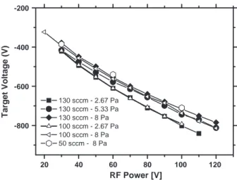
As an initial step, the behavior of the home-synthesized target ver-sus experimental deposition parameters was investigated. The evolu-tion of the self-bias target voltage is plotted versus the RF power in
the 30–120 W range (Fig. 1) for three chamber pressures in the
depo-sition chamber, 2.67 Pa, 5.33 Pa, and 8 Pa and for different values of argon flux, i.e. 50, 100 and 130 sccm. As revealed, the self-bias target voltage is ranging from 400 to 800 V, i.e. at relatively high values con-sidering the low RF power in the 30–120 W range (power density in
the 1.5 to 6 W cm− 2ranges). As displayed inFig. 1, the absolute
tar-get voltage value increases strongly while increasing the RF power from 30 to 120 W. Conversely, the target voltage depends only weak-ly on the deposition pressure. As shown, for lower deposition pres-sure ranging from 2.67 to 5.33 Pa, the self-bias target voltage appears roughly constant for a RF power in the 30–50 W range. For RF power higher than 70 W, only a weak variation is observed for the two Ar flux 130 and 100 sccm and a deposition pressure of 2.7 Pa. For higher deposition pressure values, i.e. 5.33 and 8 Pa, after a first drop, the self-target voltage does not vary significantly for the three studied Ar flux values.
For a fixed pressure in the deposition chamber, only slight varia-tion of the self-bias target voltage (variavaria-tion lower than 10 V) was observed while varying the argon flux in the 50–130 sccm range. In-deed, our deposition apparatus is not equipped with a regulated pumping valve. The deposition pressure is thus obtained by a manual adjustment of the pumping speed. In other words, the deposition pressure and the argon flux cannot be varied independently: a de-crease of the argon flux systematically leads to a pressure dede-crease in the deposition chamber. We can conclude that the RF power is a
main parameter for the GaV4S8deposition process. In our
experimen-tal conditions, the deposition pressure appears as a second order pa-rameter for pressure value below 5 Pa. Thus, in this study, only two
main experimental parameters have been considered: RF power and deposition pressure.
3.2. Deposition rate
According to the process characterization previously described, the experimental parameters were investigated for two argon flux values, 50 and 100 sccm. The deposition pressure and the RF power were varied in the 1.33 to 5.33 Pa and 60 to 100 W ranges (target power density in
the 3–5 W cm−2range).Table 1gathers a selection of samples of this
study, deposited at 5.33 Pa and a target-to-substrate distance of 5 cm, with their experimental conditions (RF power, Ar flux, target self-bias) and their main characteristics (thickness and chemical composition). The effect of Ar flux variation is illustrated by the comparison of samples B and C with samples A and D, respectively. In both cases, the variation of the target voltage is 10 V and the deposition rate variation is rather weak.
For the two Ar flow rate values, the deposition rate is increasing lin-early with the RF power applied to the target; no significant variation related to the flow rate value was evidenced. For a substrate-to-target distance of 5 cm and a deposition pressure of 5.33 Pa, the deposition
rate is varying from 3 to 6 nm min−1, when the RF power is increased
from 60 to 100 W. In the studied range of experimental parameters, the
higher deposition rate (6 nm min−1) was obtained for a RF power of
100 W, i.e. a power density of 5 W cm−2. Such low deposition rate
values are indeed related to the low power density involved in the pro-cess, leading to a low sputtered species density. These values, in the
nm min−1range, are in good agreement with our previous works
relat-ed to complex oxides[28]. Nevertheless, GaV4S8material appeared
dif-ficult to sputter, compared to the typical deposition rate observed for
magnetron sputtered materials[27,36–38].
3.3. Chemical composition
The chemical composition of deposited films was investigated by EDS analysis. The EDS atomic concentrations were arbitrarily normalized to
the vanadium content in the stoichiometric compound GaV4S8(i.e. V
atomic content fixed to 4) and expressed as follows: x:y:z for Ga:V:S, with x, y and z being the atomic content ratios G/V, 4.V/V, and S/V re-spectively. The chemical composition of studied deposited films is
given inTable 1, for a deposition pressure of 5.33 Pa, two RF powers
(60 and 100 W) and two Ar flow rates (50 and 100 sccm). As displayed, in the studied experimental conditions, the chemical composition G:V:S of as-deposited films is varying from 1:4:5 to 1.1:4:5.8, and the as-deposited films are thus all sulfur deficient. A RF power lower than 60 W and a deposition pressure lower than 2.7 Pa are both leading to a Ga:V ratio lower than 1:4, i.e. deposited films with lower Ga and/or low sulfur contents. We may assume that low sulfur atomic content is re-lated to the high volatility of sulfur atoms. In addition, for low deposition pressure, the energy of ionized species is known to be higher than at higher pressure. Indeed, in low pressure conditions, the number of colli-sions occurring in the gas phase during the transfer of sputtered atoms between the target and the substrate is statistically lower. Such condi-tions could then favor a preferential re-sputtering of the deposited film, which is consistent with a sulfur deficient chemical composition.
The variation of thickness and chemical composition in the films was investigated for two values of target-to-substrate distance (2 and 5 cm). The films were deposited on Si substrates (5 cm length) for 2 h with a RF power of 60 W, a deposition pressure of 5.33 Pa and an Ar flow rate of 100 sccm. For the higher target to substrate
dis-tance of 5 cmFig. 2the variation of the chemical composition, i.e. S/V
and Ga/V atomic ratios, and film thickness versus the position on the sample (i.e. over 2.5 cm length, starting from location just facing the target center). For this target-to-substrate distance, the thickness is varying from 400 to 300 nm (circle symbols) starting from the sam-ple center, corresponding to a 25% variation. Meanwhile, the Ga/V (open square symbols) and S/V (bold square symbols) atomic ratios are stable at 0.25 and 1.25 respectively. Compared to the targeted chemical composition (Ga:V:S= 1:4:8) the Ga/V atomic ratio is equal to the targeted one, whereas the S/V ratio is lower than expected, i.e. the films are sulfur deficient when as-deposited. For the shorter distance value (2 cm, not shown), the thickness varies from 1.2 μm to 200 nm, respectively in the sample center and sample edge, i.e. more than 80% variation. In the same time, the Ga/V atomic ratio remains stable at the stoichiometric value 0.25, whereas the S/V ratio is equal to 1.6 in the sample center and decreases to 1.35 at the sample edge, i.e. a 15% variation. Therefore, when the sample is locat-ed closer to the target, a high gradient is observlocat-ed both for the thick-ness and the sulfur content, 80% and 15% respectively. The sulfur deficiency can be attributed to the higher energy of impinging species leading to a preferential loss of the most volatile element, i.e. sulfur. Such variations, especially the gradient of the chemical composition, were considered not suitable for a further study of the process. Thus, in order to investigate the most homogeneous deposited films, the target-to-sample distance value was fixed to 5 cm in the following of this study.
20 40 60 80 100 120 -800 -600 -400 -200 130 sccm - 2.67 Pa 130 sccm - 5.33 Pa 130 sccm - 8 Pa 100 sccm - 2.67 Pa 100 sccm - 8 Pa 50 sccm - 8 Pa Target Voltage (V) RF Power [V]
Fig. 1. Variation of the target voltage as a function of applied RF power for different pressures in the vacuum chamber: 2.67 Pa, 5.33 Pa, and 8 Pa and for three argon flow values: 130 sccm, 100 sccm and 50 sccm.
Table 1
Selection of samples with experimental conditions (RF power, deposition pressure, argon flux, target voltage), their main characteristics (thickness and chemical composition) and the calculated deposition rate for a target-to-substrate distance of 5 cm.
Sample RF power (W) Pressure (mTorr) Ar flux (sccm) Target voltage (V) Thickness (nm) Deposition rate (nm min−1) Chemical composition Ga:V:S
As deposited After annealing
A 60 40 100 −530 380 3 1:4:5 1:4:8
B 60 40 50 −540 385 3.2 0.9:4:5.4 1:4:7.97
C 100 40 50 −710 690 5.75 1:4:5.8 1:4:7.95
At this stage, we have determined a window of process parameters enabling to obtain thin films but in all cases, after the deposition step, the films were all sulfur deficient and far from the targeted chemical
composition GaV4S8. In the following sections, the as-deposited and
non-stoichiometric films will be labeled GVS thin films. 4. Structural characterization
As expected, since the GVS deposited films are not stoichiometric when as-deposited, they were also amorphous, as revealed by the XRD
pattern (pattern (a) inFig. 3) where no diffraction peaks are observed.
Even when the Ga:V:S expected stoichiometry is obtained, while
depos-iting in reactive mixture (Ar/H2S), GVS thin films need to be annealed to
exhibit a crystalline structure. So, amorphous as-deposited thin films were submitted to an ex-situ annealing in a sulfur rich atmosphere. Such sulfur enrichment during a post-annealing step is often reported in literature for sulfur-based films and mainly obtained thanks to sulfur
powder addition[32,39]or under H2S gas flow rate[40]. Accordingly,
an ex-situ annealing was performed either in a tubular furnace under
hydrogen sulfide (H2S) flux or in a sealed silica tube containing sulfur
powder under a 2 Pa partial pressure. As shown inFig. 3, both annealing
atmosphere, i.e. sulfur addition and H2S flux (respectively (b) and (c)
patterns inFig. 3) lead to XRD diagrams exhibiting diffraction peaks
typical of the GaV4S8phase (pattern (d) inFig. 3) and consistent with
JCPDF file no. 01-070-3602. Therefore, the expected crystalline phase is obtained after a one hour post-annealing with sulfur addition. The obtained thin films are polycrystalline and stoichiometric.
An extensive study of the effect of annealing temperature and duration time on the crystalline quality and grain size has been conducted. XRD diagrams were recorded for various annealing conditions: in the 673 to 1023 K and 1 to 168 h ranges, respectively. Rietveld refinements and calculation of the grain size with the fun-damental approach were carried out using the crystallographic computing system JANA2006 (V. Petricek, M. Dusek, L. Palatinus).
Fig. 4 shows the result of a typical refinement performed on a
GaV4S8film submitted to a two hour annealing at 873 K in a sealed
silica tube. This refinement confirms the good crystalline quality of the deposited film and shows that the average crystallite size is of about 32–36 nm. Moreover, the Rietveld refinements performed on both powder and thin films are in excellent agreement.
Fig. 5 shows the variation of the full width at half maximum
(FWHM) of the most intense diffraction peak of the GaV4S8 phase
((400) at 2θ≈37.25°) for an annealing duration of 2 h, 5 h, 48 h and 168 h at 873 K. The annealing time is the key parameter that
gov-erns the crystallite size (Fig. 6): for annealing step at 873 K, it
in-creases from 35 nm for a 2 h annealing to about 70 nm for a longer annealing of 168 h. Conversely, we observed that the annealing tem-perature has less influence on the crystallite size: it remains in the 40 nm range for 48 h annealing at 400, 450 or 600 °C, as displayed
in the inset ofFig. 6.
At this stage of the study, only a weak evolution on both grain size and crystalline quality is observed for thin films annealed for one or two hour duration. Thus a post-deposition annealing with excess of sulfur was performed for all deposited films at 873 K for one or 2 h.
As compared to the peak intensities of the JCPDF file for GaV4S8, no
variation in relative intensities of diffraction peaks was observed. We can thus conclude that in such experimental conditions, deposited and annealed films do not exhibit any preferential crystalline orienta-tion. Furthermore, XRD patterns of annealed films exhibit diffraction peaks with higher FWHM values. As a conclusion, we can thus assume
that the polycrystalline thin films of GaV4S8are constituted of grains
with average size smaller than the reference powder.
Chemical compositions of the deposited films have been checked by EDS analysis after the annealing. As displayed in the last column
ofTable 1, despite variations of Ga/V and S/V atomic ratios before
annealing, the chemical composition of all thin films after the annealing
S/V and Ga/V ratio [-]
Thickness
Theoretical Ga/V ratio
Experimental Ga/V ratio
Experimental S/V ratio
Theoretical S/V ratio
Distance from target center [cm]
2 1 1.5 0 0.5 0 0 50 300 400 500 Film thickness [nm] 0.5 1 1.5 2
Fig. 2. Evolution of thickness (black circles and right Y axis) and chemical composition (Ga/V ratio and S/V ratio on left Y axis) for a target to substrate distance of 5 cm. The targeted values of the ratios Ga/V and S/V are represented in dashed lines. Sputtering conditions: RF power 60 W, deposition pressure 5.33 Pa, argon flow 100 sccm, deposition duration 2 h.
10 20 30 40 50
Intensity [arb. units]
(111) (200) (220) (400) (331) (420) (422) (511) (440) Powder Thin film (b) (a) (c) (d) 2θ [°]
Fig. 3. X-ray diffraction patterns of a 400 nm thick layer after deposition (a) without annealing, (b) after 1 h annealing at 873 K in sulfur rich atmosphere in silica tube (c) under H2S flow and (d) of a home-synthesized powder used as a reference.
10 20 30 40 50 60
Iobserved Icalculated Iobs - Icalc
Bragg Position
Intensity [arb. units]
2θ [°]
Fig. 4. Rietveld refinement of the XRD diagram of a 400 nm thick GaV4S8thin film annealed
step is GaV4S8, i.e. the expected stoichiometric chemical composition, in
good agreements with XRD analysis. 5. Morphology study by SEM and AFM
As a next step in thin film characterizations, the morphology of the thin films was investigated before and after the annealing step. As
published previously[30], the surface of thin film exhibits a granular
morphology before and after annealing. SEM images of the cross
section of a thin film are presented inFig. 7. The 400 nm thick thin
film was deposited in the following experimental conditions: RF power 60 W, deposition pressure 5.33 Pa, argon flow 100 sccm and annealing 1 h at 873 K in a vacuum-sealed silica tube containing sul-fur. As evidenced, a granular morphology is observed both for
as-deposited film (Fig. 7a) and annealed film (Fig. 7b). An increase
of the grain size was evidenced by AFM analysis in tapping mode (not shown). Before the annealing step, the average grain size is in the 15–20 nm range, whereas, after a one hour annealing step at 873 K, it increases in the 25–30 nm range. These grain size values are in good agreement with the average crystallite size obtained from Rietveld calculations based on XRD patterns. In addition, the av-erage surface roughness increases slightly from 2.3 nm for the as-deposited film to 3 nm after a one hour annealing step at 873 K. Such a roughness value is assumed compatible with further device applications in microelectronics. Further, a thickness variation was
observed during the annealing step. As displayed inFig. 7, the film
thickness is decreasing from 400 nm (Fig. 7a) to 340 nm after the
annealing step (Fig. 7b), leading to an average compaction of 16%.
6. HRTEM study
To get a better insight on the bulk morphology of the films, HRTEM observations were performed on films deposited on Si sub-strates before and after annealing. HRTEM images of the bulk of an
as-deposited and annealed film are given inFig. 8.Fig. 8a was taken
near the film surface and a complete amorphous structure is clearly evidenced. Whereas, a fine analysis at the bottom part of the film, i.e. in the first 5 nm near the GVS film/Si substrate interface
(Fig. 8b) allows visualizing some crystalline plans exhibiting various
crystalline orientations and a regular distribution in the bulk of the layer. Small crystallites of few nanometer size and various
orienta-tions are shown by the white arrows in Fig. 8b. As a conclusion,
when as-deposited, GVS thin films are globally amorphous but exhib-it small crystallexhib-ites located 5 nm close to the substrate, i.e. at the very beginning of the deposition. Those crystallites are too small to be detected by XRD analysis. Nevertheless, such observation could be of great interest for a further development of the deposition process. As a last issue, HRTEM image of the bulk of a GVS film after a five hour
annealing at 873 K is presented inFig. 8c. The TEM analyses are in
good agreement with previous characterizations. A bulk granular structure is indeed evidenced with average crystallite size in the 10
to 30 nm range. In the center, a GaV4S8crystallite (diameter in the
30 nm range) is clearly observed. The insert inFig. 8c gives the
Fouri-er transform of the white area of the image which reveals two inter-atomic distance values (4.9 Å and 5.5 Å), in good agreement
with a GaV4S8phase. These values are well consistent with a
crystal-line orientation according to the (110) axis.
As published previously[33,34], the electrical properties of deposited
polycrystalline GaV4S8thin layers were investigated in Au/GaV4S8/Au
MIM structures. The variation of the thin layer resistance was investigat-ed by applying at 300 K a series of ±2.5 V/10 μs pulses to the device. These results evidenced a reversible resistive switching between two
resistance states with an average switching ratio (Rhigh− Rlow)/Rlowof
about 33%. At this early stage of the study, a switching ratio up to 200– 300% was even observed at room temperature on the most basic
GaV4S8based device. These electrical characteristics were comparable
with the 1 μs writing time achieved in the most widely used flash NOR and even superior to their typical erasing times of 10 ms. Further
electri-cal characterizations are under progress on GaV4S8based MIM devices to
determine whether this material is really competitive for further applica-tion in memory devices. In particular, works have been dedicated to the evaluation of cycling endurance, impact of downscaling on writing/
erasing speed and memory window (i.e. switching ratio (Rhigh−
Rlow)/Rlow)[34]. Undoubtedly, further studies are of great interest to
evaluate the characteristics of GaV4S8for data storage applications.
7. Conclusion
GaV4S8thin films were deposited by RF magnetron sputtering
pro-cess using a low power and low pressure followed by an ex-situ annealing in sulfur rich atmosphere. In our experimental conditions, the deposition process is characterized by self-bias target voltage in the 400 to 800 V range, i.e. relatively high values considering the
in-volved power density range (1.5 to 6 W cm−2). As-deposited GaV
4S8
thin films are globally amorphous and sulfur sub-stoichiometric com-pared to the target composition. Nevertheless, HRTEM observations of as-deposited films evidenced small crystallites of few nanometer size and various orientations located in the first 5 nm close to the GVS film/Si substrate interface, i.e. at the very beginning of the deposition. Such observation could be of great interest for a further development of the deposition process. After annealing in sulfur rich atmosphere,
38.5 38 37.5 37
168h
48h
5h
2h
Intensity [arb. units] Peak (400)
36.5
2θ [°]
Fig. 5. Evolution of the full width at half maximum (FWHM) of the (400) diffraction
peak of the GaV4S8phase (at 2θ≈37.25°) for annealing durations of 2 h, 5 h, 48 h
and 168 h at 873 K. 0 50 100 150 0 20 30 40 50 60 70 80 400 450 500 550 600 0 10 20 30 40 50 60 70 80
600°C
Crystallite size [nm] Annealing Time [h] Crystallite size [nm] Annealing Temperature [°C] 48hFig. 6. Variation of crystallite size versus annealing duration at 600 °C and versus
the obtained layers are stoichiometric and exhibit a granular morphol-ogy. Rietveld refinements of XRD diagrams confirm that after annealing the thin films crystallize with the expected lacunar spinel structure. Moreover, these films are polycrystalline with a grain size in the 10– 30 nm range, as characterized by HRTEM observations, AFM measure-ments and XRD data. Our work demonstrates the potential of these polycrystalline thin layers for RRAM non-volatile memory applications. A reversible resistive switching between two resistance states was
in-deed evidenced on Au/GaV4S8/Au MIM structures with an average
switching ratio up to 200–300% at room temperature[33,34]. The
ob-served electrical characteristics are comparable with other emerging RRAM technologies and highlight the great potential of future Mott
memories based on GaV4S8.
Acknowledgments
D. Troadec at IEMN (Institut d'Electronique, Micro et Nanotechnol-ogies) from Lille (France) is gratefully acknowledged for the prepara-tion by FIB of samples for TEM observaprepara-tions. Deep acknowledgments are also due to N. Stephan (Institut des Matériaux Jean Rouxel) in Nantes for SEM observations.
References
[1] ITRS, Emerging research devices,http://www.itrs.net/Links/2011ITRS/Home2011.
htm.
[2] D.J. Frank, et al., Proc. IEEE 89 (2001) 259.
[3] K.K. Likharev, in: J. Greer, A. Korkin, J. Labanowski (Eds.), Nano and Giga Challenges in Microelectronics, Elsevier, Amsterdam, 2003, p. 27.
[4] R. Waser, M. Aono, Nat. Mater. 6 (11) (2007) 833.
[5] C. Chappert, A. Fert, F. Nguyen van Dau, Nat. Mater. 6 (11) (2007) 813. [6] S. Raoux, Annu. Rev. Mater. Res. 39 (2009) 25.
[7] R. Waser, R. Dittman, G. Staikov, K. Szot, Adv. Mater. 21 (2009) 2632. [8] A. Sawa, Mater. Today 11 (2008) 28.
[9] A. Ignatiev, N.J. Wu, X. Chen, Y.B. Nian, C. Papagianni, S.Q. Liu, J. Strozier, Phase Transitions 81 (2008) 791.
[10] J.Y. Son, Y.H. Shin, Appl. Phys. Lett. 92 (2008) 222106.
[11] L. Courtade, C. Turquat, C. Muller, J.G. Lisoni, L. Goux, D.J. Wouters, D. Goguenheim, P. Roussel, L. Ortega, Thin Solid Films 516 (2008) 4083. [12] D.S. Jeong, H. Schroeder, U. Breuer, R. Waser, J. Appl. Phys. 104 (2008) 123716. [13] K. Szot, W. Speier, G. Bihlmayer, R. Waser, Nat. Mater. 5 (2006) 312.
[14] S. Jin, T.H. Tiefel, M. McCormack, R.A. Fastnacht, R. Ramesh, L.H. Chen, Science 264 (1994) 413.
[15] A.L. Lacaita, D.J. Wouters, Phys. Status Solidi A 205 (2008) 2281. [16] J.C. Scott, L.D. Bozano, Adv. Mater. 19 (2007) 1452.
[17] R. Muller, C. Krebs, L. Goux, D.J. Wouters, J. Genoe, P. Heremans, S. Spiga, M. Fanciulli, IEEE Electron Device Lett. 30 (2009) 620.
[18] A. Ignatiev, N.J. Wu, X. Chen, S.Q. Liu, C. Papagianni, J. Strozier, Phys. Status Solidi B 243 (2006) 2089.
[19] D. Ielmini, C. Cagli, F. Nardi, Appl. Phys. Lett. 94 (2009) 063511. [20] X.A. Tran, et al., IEEE Electron Device Lett. 32 (2011) 396. [21] J. Shin, J. Park, J. Lee, et al., IEEE Electron Device Lett. 32 (2011) 958.
[22] R. Symanczyk, R. Bruchhaus, R. Dittrich, M. Kund, IEEE Electron Device Lett. 30 (2009) 876.
[23] Y. Wang, Q. Liu, S.B. Long, et al., Nanotechnology 21 (2010) 045202.
[24] C. Vaju, L. Cario, B. Corraze, E. Janod, V. Dubost, T. Cren, D. Roditchev, D. Braithwaite, O. Chauvet, Adv. Mater. 20 (2008) 2760.
[25] C. Vaju, L. Cario, B. Corraze, E. Janod, V. Dubost, T. Cren, D. Roditchev, D. Braithwaite, O. Chauvet, Microelectron. Eng. 85 (2008) 2430.
[26] L. Cario, C. Vaju, B. Corraze, V. Guiot, E. Janod, Adv. Mater. 22 (2010) 5193. [27] C. Duquenne, P.-Y. Tessier, M.-P. Besland, B. Angleraud, P.-Y. Jouan, R. Aubry, S.
Delage, M.A. Djouadi, J. Appl. Phys. 104 (2008) 063301.
100 nm
100 nm
(a)
(b)
Fig. 7. SEM images in cross section of a 400 nm thick film (a) after deposition and (b) after annealing. The thin films were sputter-deposited (RF power 60 W, deposition pressure 5.3 Pa, argon flow 100 sccm) and annealed in a vacuum-sealed silica tube containing sulfur in the optimal conditions (873 K/1 h).
(c)
5 nm
1 -1 -1 Along ( 0 1-1) 200 111(a)
(b)
10 nm
10 nm
Fig. 8. HRTEM images in cross-section of an as-deposited thin film (a) area close to the film surface and (b) near the bottom interface thin film/Si substrate (the film was deposited
in the same experimental conditions as inFig. 6). The crystallite orientations are indicated by white arrows. (c) HRTEM image of the bulk of an annealed GaV4S8thin film (5 h at
[28] M.P. Besland, H. Djani-Ait Aissa, P.R.J. Barroy, S. Lafane, P.Y. Tessier, B. Angleraud, M. Richard-Plouet, L. Brohan, M.A. Djouadi, Thin Solid Films 495 (2006) 86. [29] Y. Quéré, A. Perrin, R. Horyn, M. Sergent, Mater. Lett. 3 (1985) 340.
[30] J. Charrier, M.-L. Anne, T. Lhermite, V. Nazabal, J.P. Guin, F. Charpentier, T. Jouan, F. Henrio, D. Bosc, J.-L. Adam, J. Appl. Phys. 104 (2008) 073110.
[31] N. Lemée, M. Guilloux-Viry, A. Perrin, F. Lalu, J. Lesueur, Mater. Sci. Eng. B 72 (2000) 47.
[32] H. Hiramatsu, K. Ueda, H. Ohta, M. Orita, M. Hirano, H. Hosono, Thin Solid Films 411 (2002) 125.
[33] E. Souchier, L. Cario, B. Corraze, P. Moreau, P. Mazoyer, C. Estounes, R. Retoux, E. Janod, M.P. Besland, Phys. Status Solidi RRL 5 (2011) 53.
[34] J. Tranchant, E. Janod, L. Cario, B. Corraze, E. Souchier, J.-L. Leclercq, P. Cremillieu, P. Moreau, M.-P. Besland, Thin Solid Films 533C (2013-this issue) 81.
[35] C. Elissalde, M. Maglione, C. Estournes, J. Am. Ceram. Soc. 90 (2007) 973. [36] F. Challali, M.P. Besland, D. Benzeggouta, C. Borderon, M.C. Hugon, S. Salimy, J.C.
Saubat, A. Charpentier, D. Averty, A. Goullet, J.P. Landesman, Thin Solid Films 518 (2010) 4619.
[37] B. Abdallah, C. Duquenne, M.P. Besland, E. Gautron, P.Y. Jouan, P.Y. Tessier, J. Brault, Y. Cordier, M.A. Djouadi, Eur. Phys. J. Appl. Phys. 43 (2008) 309. [38] S. Rahmane, B. Abdallah, A. Soussou, E. Gautron, P.-Y. Jouan, L. Le Brizoual, N.
Barreau, A. Soltani, M.A. Djouadi, Phys. Status Solidi A 207 (2010) 1604. [39] Y.-T. Nien, S.-C. Tsai, I.-G. Chen, J. Cryst. Growth 287 (2006) 128.
[40] V. Weiss, W. Bohne, J. Röhrich, E. Strub, U. Bloeck, I. Sieber, K. Ellmer, R. Mientus, F. Porsch, J. Appl. Phys. 95 (2004) 7665.