HAL Id: hal-01081401
https://hal.archives-ouvertes.fr/hal-01081401
Submitted on 7 Nov 2014
HAL is a multi-disciplinary open access
archive for the deposit and dissemination of
sci-entific research documents, whether they are
pub-lished or not. The documents may come from
teaching and research institutions in France or
abroad, or from public or private research centers.
L’archive ouverte pluridisciplinaire HAL, est
destinée au dépôt et à la diffusion de documents
scientifiques de niveau recherche, publiés ou non,
émanant des établissements d’enseignement et de
recherche français ou étrangers, des laboratoires
publics ou privés.
An efficient all-optical gate based on photonic crystals
cavities and applications
Sylvain Combrié, Aude Martin, Gregory Moille, Gaëlle Lehoucq, Alfredo de
Rossi, Johann-Peter Reithmaier, Laurent Bramerie, Mathilde Gay
To cite this version:
Sylvain Combrié, Aude Martin, Gregory Moille, Gaëlle Lehoucq, Alfredo de Rossi, et al.. An efficient
all-optical gate based on photonic crystals cavities and applications. 16th International Conference
on Transparent Optical Networks (ICTON 2014), Jul 2014, Graz, Austria. pp.1 - 4,
�10.1109/IC-TON.2014.6876693�. �hal-01081401�
An efficient all-optical gate based on
Photonic Crystals Cavities and applications.
S. Combri´e
1, A. Martin
1, G. Moille
1, G.Lehoucq
1, A. De Rossi
1,
J.-P. Reithmaier
2, L. Bramerie
3, M. Gay
31
Thales Research and Technology France, Av. A. Fresnel, 91767 Palaiseau, France
2
Inst. of Nanostructure Techn. and Analytics, CINSaT, Univ. of Kassel, Heinrich-Plett-Str. 40, 34132 Kassel, Germany
3
CNRS-Foton Laboratory (UMR 6082), Enssat, BP 80518, 22305 Lannion, France
Abstract
We use two coupled photonic crystal cavities to build an all-optical gate. The control and the modulated signal are separated spectrally by about 10 nm. This device was uperated at a rate ranging from 1 to 10 GHz with maximum coupled average power of less than 1 mW in the control signal, which translates to about 100 fJ per control pulse .
I. INTRODUCTION
We have developed a technology for all-optical signal processing in integrated photonic circuits. All-optical processing here stands for optical signals controlling the transmission of optical signals. The idea behind this is to simplify the optical architectures by minimizing the need of the optical-electric conversion. All-optical interactions imply a nonlinear response, typically as a change of the refractive index proportional to the intensity of the optical field. In semiconductors, this effect requires a large optical intensity (in the scale of 1GW/cm2
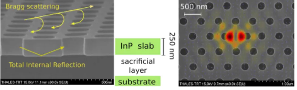
) to become noticeable, and much more in other materials, such as glass. Although optical nonlinearities are fast (in the 1 - 100 ps range), the poor energy efficiency, compared to electro-optic devices, has been considered for a long time preventing practical applications. The development of integrated photonics and, more specifically, the spread of techniques suitable for the fabrication of sub-wavelength optical structures with high precision has changed this picture drastically. In the ’90s two dimensional photonic crystals have been fabricated using a fairly standard process on silicon on insulator [1]. The optical confinement here results from the combined effect of Bragg reflection (in plane) and total internal reflection, which is particularly strong owing to the large contrast of the refractive index (fig. 1). The progress in the design of cavities[2] based on this technology led to the demonstration of single mode resonators with quality factor which have been growing up to about 9 millions[3].
The first observation of optical bistability and switching was reported in photonic crystal cavities based on silicon on oxide at NTT[4]. Here, the energy of the optical set pulse required to switch the cavity state was below 100 fJ, owing to the dramatic reduction of the volume of the optical mode about one cubic wavelength and the still large Q-factor. The physical origin of the nonlinear response is the generation of free carriers following two-photon absorption, which implies that the recovery time is related to the carrier dynamics and, particularly, recombination. This is why the typical time response of these devices is in the 100 ps range.
In 2006, we have introduced an GaAs-based PhC technology enabling high-Q resonators[5], [6], [7] and we
Fig. 1. SEM image representing the photonic crystal suspended semiconductor slab (left) and (right) top view of a cavity obtained by displacing two holes. The modal volume of this cavity is about twice the diffraction limit ((λ/2n)3
). The field distribution of the corresponding resonant mode is superimposed.
have used it to demonstrate a fast all-optical modulator[8]. Here, a recovery time as short as 6 picosecond was demonstrated, owing to the fast carrier dynamics in this material. Moreover, much stronger nonlinear absorption
in GaAs compensated for the lower loaded Q-factor designed here in order to allow a wider bandwidth than in refs. [4]. In GaAs PhCs, the surface recombination is extremely strong and this keeps the density of the photogenerated carriers to a low level. Therefore, all-optical modulation there results from the ultra-fast cross-absorption[8].
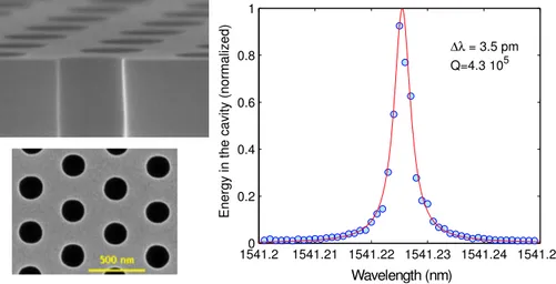
Hereafter, we focus on Indium Phosphide. The quality of the InP process is assessed in fig. 2. The largest (loaded) Q-factor measured in these samples exceeds 4105
. 1541.20 1541.21 1541.22 1541.23 1541.24 1541.25 0.2 0.4 0.6 0.8 1 Wavelength (nm) Ener gy in the cavi ty (norm alize d) ∆λ= 3.5 pm Q=4.3 105
Fig. 2. High-Q (> 0.4 million) Indium Phosphide photonic crystal cavities. High-resolution SEM image, cross section and top view. On the right, measurement of the resonance spectra and lorentzian fit.
II. SWITCHING USING PHOTONIC CRYSTAL CAVITIES AND NONLINEAR ABSORPTION
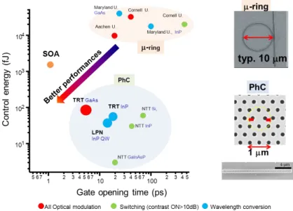
The simplest all-optical switch consists in a resonant filter, such as sketched in fig. 3, where the resonant frequency is controlled optically. In the OFF state, the wavelength carrying data is set off-resonance, and the transmission is low. Upon the arrival of the optical control pulse, the cavity is spectrally shifted to become on-resonance with the data, causing the transmission to increase. The cavity on-resonance is controlled all-optically via an intensity-dependent refractive index, which in semiconductors, is mostly related to the excitation of free carriers. Free carriers can be excited by the direct absorption of the optical ”pump”, or by non-linear absorption. In the first case, the wavelength of the pump has to be adjusted relative to the band gap of the material. The injection of the pump is not trivial in an integrated optical circuit, and advanced fabrication techniques are required to control the volume where absorption takes place. In contrast, it is very easy to control and to localize the nonlinear absorption, because this follows the localisation of the optical field. In photonic crystal cavities the nonlinear absorption can be extremely energy-efficient, which is a direct consequence of their extremely small size. The figure below attempts a comparison of a variety of experiments performed in different small
Fig. 3. Principle of all-optical modulation using a resonant cavity. The device is configured as a narrowband filter. The signal is normally detuned relative to the resonance of the cavity. The non-linear excitation (due to an optical ”pump”) induces a blue shift resulting into an increase of the transmission.
carriers are generated by linear absorption, entailing off-plane excitation through a focused beam. This said, it is apparent that the typical energy required to a pump pulse to induce an all-optical modulation is by far lower in photonic crystal cavities. It is also apparent that the fastest [8] and the most energy-efficient [9] devices exploit the properties of III-V semiconductors.
Fig. 4. Comparison of nonlinear operation (modulation, switching) in different cavity geometries and materials. Points represent the characteristic response time and operating pump energy in the pulsed regime.Colors refers to the case of all-optical modulation, inferred by a pump-probe, with low or large contrast, or wavelength conversion at> 1 GHz rate.
III. TOWARDS OPTICAL SIGNAL PROCESSING USING NANOPHOTONIC CAVITIES
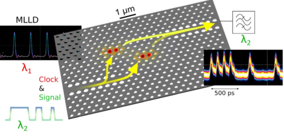
Indium Phosphide photonic crystal cavities have been demonstrated by us and by DTU [10], [11], [12] providing large switching contrast and a fairly fast dynamics, with a typical two time constant relaxation, first observed by NTT in silicon and InGaAsP PhC cavities[9]. In this talk we will focus on the properties of the so-called ”photon molecules”, resulting form the coupling of two photonic cavities. We discuss dynamics, all-optical modulation and frequency conversion at a fast repetition rate (10 GHz). [10]. The interest in the PhC/InP approach has been confirmed by the recent results from DTU, who demonstrated all-optical signal processing[13] and LPN, who introduced hybrid Silicon-InP cavities and demonstrated fast processing[14]. In Fig.5, we show the device and the signals used to drive it: the control signal comes from a prototype modelocked diode laser build by Alcatel-Lucent-Thales III-V labs operating at 10 GHz and providing 2 ps long pulses. The centre wavelength was tuned to one of the two resonances. The second signal is obtained by modulating a CW laser (tuned close to the other resonance) with a pseudorandom sequence synchronized with the control signal. The average power the two signals is comparable and it is about 1 mW. The output is filtered (to remove the control), amplified and detected using a fast photodiode (40 GHz) and a 70 GHz sampling oscilloscope. The result is again a pseudorandom sequence but sampled by the pulses of the modelocked source. In this talk we will detail the technology and the experimental procedure. We will also compare this technology and experiment with the other approaches discussed above.
IV. CONCLUSION
By leveraging on the high-quality Indium Phoshpide photonic crystal technology (maximum Q> 400000), we demonstrate all-optical signal processing at a rate of 10 GHz. Moreover, operation are energy-efficient, because it is estimated that the device uses about 100 fJ per control pulse.
This work was supported by the COPERNICUS project (grant no. 249012) and by the AUCTOPUSS project funded by the French Research Agency (ANR). We thank A. Shen (Alcatel-Lucent-Thales III-V labs) for kindly providing us with the modelocked diode laser.
REFERENCES
[1] T. Krauss, R. De La Rue, and S. Brand, “Two-dimensional photonic-bandgap structures operating at near-infrared wavelengths,” Nature, vol. 383, no. 6602, pp. 699–702, 1996.
[2] Y. Akahane, T. Asano, B. Song, and S. Noda, “High-q photonic nanocavity in a two-dimensional photonic crystal,” Nature, vol. 425, no. 6961, pp. 944–947, 2003.
[3] H. Sekoguchi, Y. Takahashi, T. Asano, and S. Noda, “Photonic crystal nanocavity with a q-factor of 9 million,” Opt. Express, vol. 22, no. 1, pp. 916–924, Jan 2014.
Fig. 5. Processing using an InP photonic molecule. Wavelength conversion and ”and” gate function by mixing a on/off signal with a periodic train of pulses at a rate of 10 GHz. Oscilloscope traces of the input and output signals are represented togheter with the layout of the device.
[4] T. Tanabe, M. Notomi, S. Mitsugi, A. Shinya, and E. Kuramochi, “Fast bistable all-optical switch and memory on a silicon photonic crystal on-chip,” Optics letters, vol. 30, no. 19, pp. 2575–2577, 2005.
[5] E. Weidner, S. Combri´e, N.-V.-Q. Tran, A. De Rossi, J. Nagle, S. Cassette, A. Talneau, and H. Benisty, “Achievement of ultrahigh quality factors ingaas photonic crystal membrane nanocavity,” Applied Physics Letters, vol. 89, pp. 221 104–221 104, 2006. [6] S. Combri´e, A. De Rossi, Q. V. Tran, and H. Benisty, “gaas photonic crystal cavity with ultrahigh q: microwatt nonlinearity at
1.55µm,” Optics Letters, vol. 33, pp. 1908–1910, 2008. [Online]. Available: http://dx.medra.org/10.1364/OL.33.001908
[7] S. Combrie, N. Tran, A. De Rossi, C. Husko, and P. Colman, “High quality gainp nonlinear photonic crystals with minimized nonlinear absorption,” Applied Physics Letters, vol. 95, pp. 221 108–221 108, 2009.
[8] C. Husko, S. Combri´e, Q. V. Tran, C. W. Wong, and A. D. Rossi, “Ultra-fast all-optical modulation ingaas photonic crystal cavities,” Applied Physics Letters, vol. 94, p. 021111, 2009.
[9] K. Nozaki, T. Tanabe, A. Shinya, S. Matsuo, T. Sato, H. Taniyama, and M. Notomi, “Sub-femtojoule all-optical switching using a photonic-crystal nanocavity,” Nature Photonics, vol. 4, no. 7, pp. 477–483, 2010.
[10] S. Combri´e, G. Lehoucq, A. Junay, S. Malaguti, G. Bellanca, S. Trillo, L. M´enager, J. P. Reithmaier, and A. De Rossi, “All-optical signal processing at 10 ghz using a photonic crystal molecule,” Applied Physics Letters, vol. 103, no. 19, p. 193510, 2013. [11] M. Heuck, S. Combri´e, G. Lehoucq, S. Malaguti, G. Bellanca, S. Trillo, P. T. Kristensen, J. Mørk, J. Reithmaier, and A. de Rossi,
“Heterodyne pump probe measurements of nonlinear dynamics in an indium phosphide photonic crystal cavity,” Applied Physics Letters, vol. 103, no. 18, p. 181120, 2013.
[12] Y. Yu, E. Palushani, M. Heuck, N. Kuznetsova, P. T. Kristensen, S. Ek, D. Vukovic, C. Peucheret, L. K. Oxenløwe, S. Combri´e et al., “Switching characteristics of an inp photonic crystal nanocavity: Experiment and theory,” Optics Express, vol. 21, no. 25, pp. 31 047–31 061, 2013.
[13] D. Vukovic, Y. Yu, M. Heuck, S. Ek, N. Kuznetsova, P. Colman, E. Palushani, J. Xu, K. Yvind, L. Oxenloewe et al., “Wavelength conversion of a 9.35 gb/s rz ook signal in an inp photonic crystal nanocavity,” Photonic Technology Letters, vol. 26, p. 257, 2014. [14] A. Bazin, K. Lengl´e, M. Gay, P. Monnier, L. Bramerie, R. Braive, G. Beaudoin, I. Sagnes, R. Raj, and F. Raineri, “Ultrafast all-optical
switching and error-free 10 gbit/s wavelength conversion in hybrid inp-silicon on insulator nanocavities using surface quantum wells,” Applied Physics Letters, vol. 104, no. 1, p. 011102, 2014.