HAL Id: hal-01169596
https://hal.archives-ouvertes.fr/hal-01169596
Submitted on 29 Jun 2015
HAL is a multi-disciplinary open access
archive for the deposit and dissemination of
sci-entific research documents, whether they are
pub-lished or not. The documents may come from
teaching and research institutions in France or
abroad, or from public or private research centers.
L’archive ouverte pluridisciplinaire HAL, est
destinée au dépôt et à la diffusion de documents
scientifiques de niveau recherche, publiés ou non,
émanant des établissements d’enseignement et de
recherche français ou étrangers, des laboratoires
publics ou privés.
Printed Circuit Board Permittivity Measurement Using
Waveguide and Resonator Rings
Sjoerd Op ’T Land, Olga Tereshchenko, Mohamed Ramdani, Frank Leferink,
Richard Perdriau
To cite this version:
Sjoerd Op ’T Land, Olga Tereshchenko, Mohamed Ramdani, Frank Leferink, Richard Perdriau.
Printed Circuit Board Permittivity Measurement Using Waveguide and Resonator Rings. EMC’14,
May 2014, Tokyo, Japan. �hal-01169596�
Printed Circuit Board Permittivity Measurement
Using Waveguide and Resonator Rings
Sjoerd Op ’t Land
⇤, Olga Tereshchenko
†, Mohamed Ramdani
⇤, Frank Leferink
†and Richard Perdriau
⇤ ⇤Department of Electronics, Ecole Superieure d’Electronique de Ouest, Angers, FranceEmail: {sjoerd.optland, mohamed.ramdani, richard.perdriau}@eseo.fr
†Telecommunication Engineering Group, Faculty of EEMCS, University of Twente, The Netherlands
Email: {o.tereshchenko, f.b.j.leferink}@utwente.nl Abstract—Knowing the frequency dependent complex
permit-tivity of Printed Circuit Board (PCB) substrates is important in modern electronics.
In this paper, two methods for measuring the permittivity are applied to the same Flame Resistant (FR4) substrate and the re-sults are compared. The reference measurement is performed by inserting the sample in a rectangular waveguide and measuring the scattering parameters. The other measurement is performed by etching a microstrip ring resonator on the same substrate and measuring the scattering parameters. The results are similar and suggest isotropy and homogeneity.
Index Terms—PCB, FR4, substrate, permittivity, material characterisation, microstrip, waveguide, resonator ring
I. INTRODUCTION
The permittivity " relates the displacement of charges D in a linear and homogeneous material with the electric field E as follows:
Dej!t⌘ "0"rEej!t, (1)
where the relative permittivity "r is a second rank tensor in
general, which reduces to a scalar for isotropic materials. Conventionally, the real and imaginary parts are denoted as follows:
"r= "0r j"00r. (2)
Under above sign conventions, "0r quantifies the energy storage
in the material and "00r quantifies the loss.
Most modern electronics are based on PCBs of the FR4 class for economical and mechanical reasons. An FR4 substrate consist of a woven fiberglass cloth, filled with epoxy resin: a composite, non-homogeneous material. The dielectric permittivity of FR4 substrates is often not guaranteed, and only typical values are given by manufacturers (e.g. [1]). In the design of modern electronics, knowing the complex substrate permittivity is important. For example, it is attrac-tive to integrate antennas with the transceiver electronics on the same substrate. The real permittivity of the substrate "0r determines the resonance frequency, while the imaginary
permittivity "00r determines the quality factor Q. To produce a
first-time right Radio Frequency Identification (RFID) antenna for 866 869 MHz, a ±0.7% tolerance on real substrate permittivity is acceptable.
As another example, the substrate between power and ground planes plays an important role in the power distribution
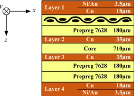
y x z Cu 18µm Prepreg 7628 180µm Cu 35µm Layer 2 Core 710µm Cu 35µm Layer 3 Prepreg 7628 180µm Prepreg 7628 180µm Cu 18µm Ni/Au 3.5µm Ni/Au 3.5µm Layer 4 Layer 1
Figure 1. Eurocircuits standard 4-layer stackup with material directions: weft-or x-direction, warp- weft-or y-direction, and depth- weft-or z-direction.
network (PDN) of a PCB. When using the substrate as a two-dimensional waveguide and terminate it all around the circuit with its characteristic impedance [2], the substrate permittivity may not deviate too much in either way. Suppose that ±5% reflection from a given ESR is allowable; then it can be shown that about ⌥20% variation in the real substrate permittivity "0r
is tolerable.
So, depending on the application, the permittivity of PCB substrates needs to be known more or less precisely: from tenths to tens of percents.
In this article we will look at a typical research case: occa-sional measurements of FR4 permittivity to create matched circuits. We target 10% measurement accuracy. The standard Eurocircuits 4-layer stack-up of Figure 1 was used. Both core and prepreg consist of Technolam NP-155F [1].
The prepreg and core are both composite materials consist-ing of fibre glass fabric ("r⇡ 5) in epoxy resin ("r⇡ 3.2). The
fabric consists of straight warp yarns in the y-direction, with weft yarns going up and down in the x-direction.
We will start by giving an overview of existing measurement methods in section II. From these methods, we will use an established method to take a reference measurement on a sample in section III. Alternatively, we will apply a more experimental method in section IV. We will compare both methods and outline future research in section V.
II. STATE OF THEART
A complete overview of all existing measurement methods is outside the scope of this article. Yet, a simple classification
z x y
E(x)
(a) Photo of the MUT sample in rectangular waveguide, with super-imposed E-field profile.
1
2
(b) Microstrip ring resonator excited with 5 = 2⇡r. The clockwise- and counterclockwise wave amplitudes are superimposed on the artwork.
Figure 2. Field structure for both measurement methods.
can be made: resonant- and non-resonant methods. Resonant methods work for a finite number of frequencies and accu-rately measure even small losses ("00
r). Non-resonant methods
are broadband and only measure high losses accurately. [3] Examples of resonant methods are the resonant cavity, the Fabry-Perot resonator, the open (or Courtney) resonator, Full Sheet Resonance (FSR) [4], planar resonators pressed against or between samples [5]. Examples of non-resonant methods are the coaxial probe, the parallel-plate set-up, transmission line (planar [6], coaxial or rectangular [7], [8]) and free-space measurement. These methods all require a fixture: something that couples guided waves to a known geometry containing the Material Under Test (MUT). A recurring problem is the presence of air gaps between fixture and MUT. [3], [9] Our material has the form of a smooth, flat and solid sheet, which can be easily machined in a shape of rectangular sample. We are interested the permittivity of this material over a broad frequency range. As the rectangular dielectric waveguide (RDWG) is an established method and the rectan-gular waveguides are readily available in our laboratory, it was chosen as the reference measurement. It is a banded method: samples of different sizes need to be cut out for insertion in waveguides of different bandwidths.
Alternatively, we choose a planar ring resonator [10], [11] to evaluate the possibility to measure accurately without special fixtures. It is a resonant method, so only a few frequency samples of the permittivity will be available.
III. REFERENCEMEASUREMENT
The Rectangular Dielectric Waveguide (RDWG) method consists of measuring the S -parameters of an rectangular waveguide with and without the MUT sample, cf. Figure 2a. A software algorithm then solves for the complex permittivity "r.
We fabricated samples for the available rectangular waveg-uide sections for the S, C and X band [8]. As can be seen in Figure 2a, the wave only ‘feels’ the vertical component of the
Table I
MATERIAL PROPERTY CALCULATION ALGORITHMS AVAILABLE IN THE
AGILENT85071ESOFTWARE PROGRAMME
Method Calculates Best for. . . Particularities 1.
Nicolson-Ross "r& µr magnetic, shortor lossy MUTs Fast, but hasdiscontinuities. 2. Reflection/ Transmission Epsilon Pre-cision Model "r (µr⌘ 1) non-magnetic materials, long, low-loss MUTs Accurate, no discontinuities. 3. Transmis-sion Epsilon Fast Model "r (µr⌘ 1) non-magnetic materials, long, low-loss MUTs Similar to precision but faster and better for lossy MUTs.
permittivity tensor "r,yy, mainly in the middle of the sample.
To also measure the horizontal component "r,xx, we fabricated
rotated samples from the same substrate for the C- and X-band. Notice, because of the field profile, that air gaps at the left and right end of the sample hardly impact the measurement result. Next, we measured the S -parameters with an HP 8510C VNA at 21 and 30% relative humidity. We repeated the measurement for all three bands, using rotated samples if available: 5 measurements in total.
Finally, we needed to derive the complex permittivity from this measurement data. Three algorithms in the Agilent 85071E software are available as outlined in Table I. Note that these algorithms all implicitly suppose an isotropic and homogeneous MUT, while it is not.
As our samples are non-magnetic, short, and have medium loss, Table I shows that none of the three available methods is an obvious match. Therefore, we tried all three, cf. Figure 3. Model 1, that of Nicolson-Ross [12], is suitable only for magnetic materials when the measured value of S11 never
approaches zero. Otherwise the results are in error. Note that this method does not converge on our S-band data.
Model 2, the Reflection/Transmission Epsilon Precision Model [13] uses all four measured S -parameters to determine the permittivity, assuming the material to be non-magnetic. This eliminates the need to know the position of material in a sample holder.
Model 3, the Transmission Epsilon Fast Model is minimis-ing the difference between the measured value of transmission coefficient and computed value. It is forcing the magnetic permeability µr⌘ 1. This also gives an error for the imaginary
part of permittivity in the X-band. It becomes negative, thereby suggesting gain, which does not correspond to reality.
All three models show that this material has low losses and a permittivity close to 5 which was expected. We choose model 2, because it gives physically plausible results for all bands and because of its robustness against positioning errors.
IV. RESONATORRING
Consider the microstrip ring resonator depicted in Figure 2b. It consists of a microstrip ring, which supports a clockwise-and a counterclockwise propagating wave. Two microstrip feeds, spaced 90 apart, are capacitively coupled to the ring.
3.8 4.0 4.2 4.4 4.6 4.8 2 4 6 8 10 12 1. Nicolson-Ross 2. R/T Epsilon Precision 3. T Epsilon Fast ... Frequency (GHz) Re al pe rm it ti vt y 13 2 1 3 2 3 2
(a) The real part of the permittivity.
-0.2 -0.0 0.2 0.4 0.6 0.8 1.0 1.2 2 4 6 8 10 12 1. Nicolson-Ross 2. R/T Epsilon Precision 3. T Epsilon Fast ... Im agi na ry pe rm it ti vt y Frequency (GHz) 3 2 3 1,2 3 1,2
(b) The imaginary part of the permittivity, representing the losses. Figure 3. The complex permittivity of the y-direction samples, calculated with the different methods.
Imagine that power coming from port 1 equally splits into a clockwise- and a counterclockwise propagating wave. If the circumference 2⇡r equals an odd multiple of the wavelength (like in the figure), both waves interfere destructively at the feed point of port 2, therefore S21 is minimum. If the
circumference equals an even multiple of the wavelength, there is constructive interference, hence S21 is maximum.
By measuring the resonance frequencies (the local maxima of S21) the phase velocity v and the real effective permittivity
"r,eff can be calculated:
v = f =2⇡r
k f k = 2,4,6,... (3) "r,eff = ⇣ cv0
⌘2
, (4)
where k is the harmonic index and r is the effective radius of the ring.
Finally, a microstrip model needs to be used to obtain the real substrate permittivity "0
r, knowing "r,effand the trace
cross-sectional geometry.
Note that the imaginary permittivity can also be measured using this method, by measuring the quality factor Q, which represents the total resonator loss. However, to be accurate, radiation and conductor losses must also be known and sub-tracted and there is no simple analytical relation to do so. Therefore, we will not extract the imaginary permittivity. This method for measuring the permittivity has several metro-logical advantages. First, there are no fringing fields at the ends that need to be taken into account.
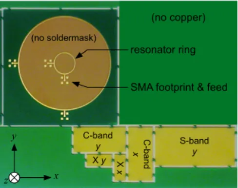
resonator ring SMA footprint & feed (no soldermask) S-band y C-band y C-b an d x X x X y (no copper) z x y
Figure 4. Panel containing both the resonator rings and substrate samples for the RDWG measurement method.
Secondly, only few quantities need to be known precisely (cf. (3)). As the ring is sufficiently large with respect to the trace width (r/w > 7), the wave travels the centreline of the annular ring [14]. Therefore, under- or overetching of the PCB can be neglected. The uncertainty of the resonance frequency
f measured with a VNA is known and small.
Thirdly, the microstrip turns rotates with respect to FR4 fabric orientation, so the average "r is found. The field is
mostly perpendicular to the substrate, so we find "r,zz, the
interesting value for matching traces.
Lastly, as the feeds are quite short and matched, there is no need for de-embedding.
The test panel of Figure 4 was laid out using a Python script and PyPCB [15] in order to explicitly document layout decisions. Two resonator rings were made with 1.91 cm and 8.38 cm respective diameters, targeting overlapping resonance frequencies on a reasonable PCB surface. The microstrip was placed on outer layer 1, with a ground plane on layer 2 (cf. Figure 1). Surface mount SMA connectors were soldered onto the resonator feeds using reflow soldering. No solder mask was present on the substrate samples as well as on the rings. Consequently, the rings have a gold finish. The S21 parameter of both rings was measured using an
Agilent N5247A network analyser, after calibration up to the SMA connectors. The frequency was swept from 10 MHz to 12 GHz on the large ring, from 2 GHz to 26 GHz on the small ring, both with 801 points.The resonances were manually identified and the frequency (on the 801-point scale) of the local maxima are tabulated in Table II for both rings. Notice that from the 12th harmonic upward, another mechanism seems to obscure the ring resonances. On the small ring, a similar effect appeared after the 4th harmonic, but left the 6th and 8th distinguishable. The QTEM cut-off frequency of this microstrip is [16]:
fMS,TEM⇡ 21.3 GHz · mm
(w + 2h)p"r+1 ⇡ 6.4GHz, (5)
so resonances above that frequency are less and less meaning-ful.
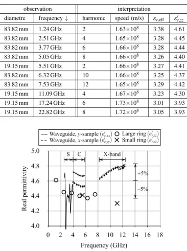
Table II
OBSERVED RESONANCES USING THE TWO MICROSTRIP RING RESONATORS
observation interpretation
diametre frequency # harmonic speed (m/s) "r,eff "0r,zz 83.82 mm 1.24 GHz 2 1.63⇥108 3.38 4.61 83.82 mm 2.51 GHz 4 1.65⇥108 3.28 4.45 83.82 mm 3.77 GHz 6 1.66⇥108 3.28 4.44 83.82 mm 5.05 GHz 8 1.66⇥108 3.26 4.40 19.15 mm 5.51 GHz 2 1.66⇥108 3.27 4.41 83.82 mm 6.32 GHz 10 1.66⇥108 3.25 4.37 83.82 mm 7.53 GHz 12 1.65⇥108 3.29 4.42 19.15 mm 11.09 GHz 4 1.67⇥108 3.23 4.30 19.15 mm 17.24 GHz 6 1.73⇥108 3.01 3.93 19.15 mm 22.82 GHz 8 1.72⇥108 3.05 3.93 4,0 4,2 4,4 4,6 4,8 5,0 0 2 4 6 8 10 12 14 16 18 Re al pe rm it ti vi ty Frequency (GHz) +5% –5% S C X-band 5.0 4.8 4.6 4.4 4.2 4.0 Frequency (GHz) Waveguide, y-sample Waveguide, x-sample Large ring Small ring "0 r,xx "0 r,yy "0r,zz "0 r,zz
Figure 5. Permittivity measured using waveguide and resonator methods.
Using ADS LineCalc, we reverse-calculated the substrate "0r for a measured "r,eff at a given frequency. The resulting
permittivities are added to Table II and compared with the reference measurement (RDWG) results in Figure 5.
V. CONCLUSIONS ANDRECOMMENDATIONS
In this paper, we studied the permittivity of a 4-layer, standard FR4 substrate. We measured the complex permittivity in the plane of the substrate ("r,xx and "r,yy) of the entire
stackup using the RDWG method. We measured the real permittivity perpendicular to the substrate ("0
r,zz) of the prepreg
between layer 1 and 2 using a microstrip ring resonator. The RDWG method seems to be imprecise in the S-band, because the sample is very short with respect to the wave-length. The transmission epsilon model used to calculate the complex permittivity from the measured scattering parameters seems to perform best. Only the Reflection/Transmission Ep-silon Precision model gives physical permittivities for all three bands. The advantage of this method is that it can be performed with readily available rectangular waveguide sections.
The microstrip ring resonator measurement yielded real permittivity values that did not differ significantly between two resonator rings with a different diameter. No imaginary
permittivity values could be easily extracted, however. The advantage of this method is that it directly measures the "0r,zz
permittivity, which is the tensor component that matters for PCB design.
The obtained values vary with frequency between 4.3 and 4.8. Supposing material isotropy (" ⌘ "xx ⌘ "yy⌘ "zz) and
homogeneity between the layers, the permittivities measured with both methods should be equal. Under that condition only, the difference between permittivities obtained with both methods equals the relative measurement error between the two methods. In the X-band, both methods correspond to within 12%, which is slightly worse than our objective. In the C-band, both methods correspond to within 5%, which was our initial objective.
REFERENCES
[1] Datasheet NP-155F, Technolam, 2011. [Online]. Avail-able: http://technolam.de/cms/upload/datenblaetter en/Datasheets NP-155F E-4-2011.pdf
[2] M. Coenen and A. van Roermund, “Resonant-free PDN designR,” in Electromagnetic Compatibility of Integrated Circuits (EMC Compo), 2011 8th Workshop on, 2011, pp. 207–212.
[3] J. Krupka, “Frequency domain complex permittivity measurements at microwave frequencies,” Measurement Science and Technology, vol. 17, no. 6, p. R55, 2006. [Online]. Available: http://stacks.iop.org/ 0957-0233/17/i=6/a=R01
[4] Non-destructive Full Sheet Resonance Test for Permittivity of Clad Laminates, IPC Std. 2.5.5.6, may 1989. [Online]. Available: http://www.ipc.org/4.0 Knowledge/4.1 Standards/test/2.5.5.6.pdf [5] D. L. Wynants, “Dk or dielectric constant or relative permittivity
or "r: What is it, why is it important and how does Taconic test for it?” Taconic ADD, Tech. Rep., 2011. [Online]. Available: http: //www.taconic-add.com/pdf/technicaltopics--dielectric constant.pdf [6] A. Rakov, M. Koledintseva, J. Drewniak, and S. Hinaga, “Major error
and sensitivity analysis for characterization of laminate dielectrics on PCB striplines,” in IEEE Symp. Electromag. Compat., Denver, CO, aug 2013.
[7] Z. Abbas, R. D. Pollard, and R. Kelsall, “A rectangular dielectric waveguide technique for determination of permittivity of materials at W-band,” Microwave Theory and Techniques, IEEE Transactions on, vol. 46, no. 12, pp. 2011–2015, 1998.
[8] O. V. Tereshchenko, F. J. Buesink, and F. B. Leferink, “Measurement of complex permittivity of composite materials using waveguide method,” in EMC Europe 2011 York, sep 2011, pp. 52 –56.
[9] “Basics of measuring the dielectric properties of materials,” Agilent, Tech. Rep., apr 2013. [Online]. Available: http://cp.literature.agilent. com/litweb/pdf/5989-2589EN.pdf
[10] J. Vorl´ıˇcek, J. Rusz, L. Oppl, and J. Vrba, “Complex permittivity measurement of substrates using ring resonator,” in Technical Computing Bratislava, 2010. [Online]. Available: http://phobos.vscht. cz/konference matlab/MATLAB10/full text/107 Vorlicek.pdf [11] C.-C. Yu and K. Chang, “Transmission-line analysis of a capacitively
coupled microstrip-ring resonator,” Microwave Theory and Techniques, IEEE Transactions on, vol. 45, no. 11, pp. 2018 –2024, nov 1997. [12] A. Nicolson and G. F. Ross, “Measurement of the intrinsic properties
of materials by time-domain techniques,” Instrumentation and Measure-ment, IEEE Transactions on, vol. 19, no. 4, pp. 377–382, 1970. [13] J. Baker-Jarvis, E. Vanzura, and W. Kissick, “Improved technique
for determining complex permittivity with the transmission/reflection method,” Microwave Theory and Techniques, IEEE Transactions on, vol. 38, no. 8, pp. 1096–1103, 1990.
[14] I. Rosu, “Microstrip, stripline, and CPW design,” Tech. Rep., apr 2012. [Online]. Available: http://www.qsl.net/va3iul/Microstrip Stripline CPW Design/Microstrip Stripline and CPW Design.pdf [15] “PyPCB – specifying PCB layout in Python,” nov 2012. [Online].
Available: http://github.com/eseo-emc/pypcb/wiki
[16] R. K. Hoffmann, Handbook of microwave integrated circuits. Norwood, MA, Artech House, Inc., 1987, vol. 1.