Microcrystalline silicon deposited from SiF4/H2/Ar plasmas and its application to photovoltaics
Texte intégral
Figure


Documents relatifs
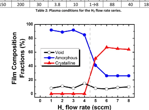
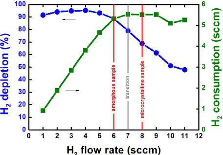
A series of microcrystalline samples was deposited by the very high frequency glow discharge VHF-GD technique, with various input powers while keeping all the other parameters
It has been observed [4,11] that, in the case of a series of slightly doped a-Si:H layers, the l 0 s R products of the majority and minority carriers, when plotted as a function of
The FTIR photocurrent spectroscopy as intro- duced here is a fast and very sensitive method for spectral measurement of the optical absorption coefficient aðEÞ, connected with
This model reproduces most of the features of the complex microstructure of microcrystalline silicon: transition from amorphous to crystalline phase, conical shape of the
Indeed, if one uses SnO 2 -clad glass substrates (Asahi type U) for micromorph tandem cells, the bottom cell thickness must be approximately 1 mm (or more) thicker, in order to
These n- and especially p-type mc-Si:H layers are presently used, both by research laboratories and by production lines, for incorporation within pin-type thin-film silicon solar
Results have shown that microcrystalline silicon can be deposited uniformly on a large area substrate with a deposition rate of more than 10 ˚A=s with a low powder formation and
Solar cells based on plasma-deposited hydrogenated microcrystalline silicon ( mc-Si:H ) as well as ‘micro- morph’ ( mc-Si:Hy a-Si:H ) tandem solar cells — both pioneered by
