HAL Id: hal-01300890
https://hal-univ-rennes1.archives-ouvertes.fr/hal-01300890
Submitted on 3 May 2016
HAL is a multi-disciplinary open access
archive for the deposit and dissemination of
sci-entific research documents, whether they are
pub-lished or not. The documents may come from
teaching and research institutions in France or
abroad, or from public or private research centers.
L’archive ouverte pluridisciplinaire HAL, est
destinée au dépôt et à la diffusion de documents
scientifiques de niveau recherche, publiés ou non,
émanant des établissements d’enseignement et de
recherche français ou étrangers, des laboratoires
publics ou privés.
Characterisation and analytical modeling of GaN
HEMT-based varactor diodes
Abdelaziz Hamdoun, L. Roy, Mohamed Himdi, Olivier Lafond
To cite this version:
Abdelaziz Hamdoun, L. Roy, Mohamed Himdi, Olivier Lafond. Characterisation and analytical
mod-eling of GaN HEMT-based varactor diodes. Electronics Letters, IET, 2015, 51 (23), pp.1930-1932.
�10.1049/el.2015.2362�. �hal-01300890�
1
Characterization and Analytical Modeling
of GaN HEMT-Based Varactor Diodes
A. Hamdoun, L. Roy, M. Himdi and O. Lafond
Varactor diodes fabricated in 0.5 µm and 0.15 µm GaN HEMT processes are modeled. The devices were characterized via DC and RF small-signal measurements up to 20 GHz, and fitted to a simple physical equivalent circuit. Approximate analytical expressions containing empirical coefficients are introduced for the voltage dependency of capacitance and series resistance. The analytical solutions agree remarkably well with the experimentally extracted C-V curves and can be used as a general model to represent the nonlinear behavior of GaN based varactors devices.
Introduction: Over the last few years, as a result of advanced heterostructure device design, GaN based semiconductors have demonstrated outstanding performance when compared to other wide band-gap semiconductor technologies [1]. Large power handling capability and high frequency operation are now achievable with good efficiency and linearity. GaN-based HEMT semiconductor devices are no longer limited to RF power amplifier applications, having been extended to other applications such as mixers, phase shifters etc. Furthermore, reconfigurable RF circuits, with high power/frequency, and excellent linearity, are in great demand. Varactors are key components in the design of these circuits. Many GaN varactors have previously been reported, mostly employing a Schottky barrier contact [2] or Metal-Semiconductor-Metal (MSM) junction [3]. In order to achieve good performance, the devices required special epitaxial layers. In this work, a standard HEMT process is employed for varactor realization. We investigate and model the equivalent capacitance CEq
and the equivalent series resistance REq of the varactor, when the overall
impedance is considered as a simple series RC circuit.
Device design and NRC GaN process: Fig. 1 shows a simplified cross-section of the epitaxial layers of the GaN HEMT process developed by the National Research Council (NRC) of Canada. The GaN500 and GaN150 processes have gate lengths of 0.5 μm and 0.15 μm, respectively. As depicted in Fig. 2, the drain and source terminals of a HEMT device are connected, thus realizing a GaN heterojunction barrier varactor diode without changing the epitaxial masks and layers of the GaN process.
Fig. 1 Schematic cross-section of HEMT, showing contacts and epitaxial
layers, and physical origin of equivalent circuit at pinch-off (VG=-3.75V).
Fig. 2 (left) HEMT electric elements configured as varactor (right)
W40L0.5 device in microwave probable test structure.
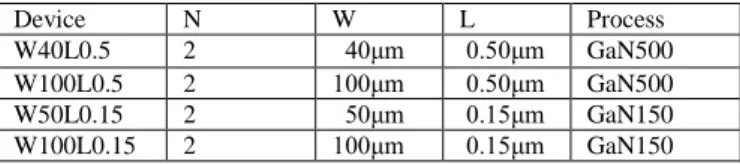
To develop a simple accurate small-signal model, four samples are studied, as detailed in Table 1. Where N is the number of fingers, W and L are the width and the length of finger.
Table 1: GaN Devices Details
Device N W L Process
W40L0.5 2 40μm 0.50μm GaN500 W100L0.5 2 100μm 0.50μm GaN500 W50L0.15 2 50μm 0.15μm GaN150 W100L0.15 2 100μm 0.15μm GaN150 Analysis of Equivalent Circuit model: The physical origins of the varactor device’s equivalent model are shown in Fig. 1. Rg, Lg, Rd, Ld,
Rs and Ls are, respectively, the metal resistance and the parasitic
inductance of the gate, of the drain and of the source. Rcst is the constant
resistor and is determined by the AlGaN layer thickness. Rsheet refers to
the constant channel resistance. Rdep and Cdep represent the resistance
and capacitance under the depletion region, which are affected by the bias voltage, VG, and change slightly when the channel starts to deplete.
The circuit of Fig. 1 can be transformed to a simple model, as in Fig. 3.
Fig. 3 Varactor equivalent circuit model
Lpara, REq, CEq and RLeak are respectively the parasitic inductor, the
equivalent series resistor, the equivalent series capacitance and the leakage resistor (~10GΩ). As can be seen in Figs. 4-5, an excellent match between the experimental and the simulated results is achieved.
Fig. 4 Measured (lines) and Modeled (Dot) S-parameters [0.1-20] GHz
Fig. 5 Measured (lines) and Modeled (Dot) S-parameters [0.1-20] GHz
Analytical Expressions of REq and CEq: At an operating frequency f, the
CEq values were extracted from the Y-parameters using the equation (1).
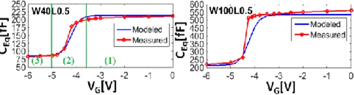
For both GaN500 and GaN150, the extracted equivalent capacitance values versus VG are shown in Figs. 6-7 (red dotted lines). In order to
describe the nonlinear behavior of CEq and of REq, analytical equations
based on empirical coefficients are derived from the measurements. Describing the behavior of CEq:
The exponential of tangent hyperbolic function yields an approximate analytical expression for CEq versus VG. It is seen that (2) accurately
describes the dependency of junction capacitance upon applied reverse bias, VG, for all characterized devices.
2
Describing the behavior of REq:
The REq-VG characteristics is a Gaussian form, as deduced from Figs.
8-9 (red dotted lines). Thus the REq-VG characteristics are taken to be:
Where A is the finger area. The parameters M, K and Y can be adjusted to properly fit the CEq and REq equations to the measured characteristics
of an arbitrary varactor size. According to Matlab simulations, the values of M, K and Y can be fixed, respectively, as 1.2, 40 and 14 for GaN500 devices and as 0.45, 20 and 4.75 for GaN150 devices. The modeled curves are plotted in Figs. 6-7-8-9 (blue lines). All of these equations are dependent only on finger geometry (number, width and length of fingers) and on VG. Equation (2) illustrates the behavior of CEq
for GaN500 and GaN150 devices, (4) describes REq for GaN500
devices, while (5) describes REq for GaN150 devices. These equations
describe the experimental results adequately under small signal. From Figs. 6-7, all CEq-VG curves exhibit the same general behavior,
which can be separated into three regions: range (1) for VG above
-3.75V, range (2) for -4.5V≤ VG ≤-3.5V and range (3) for VG < -4.75 V.
Fig. 6 Extracted and Simulated CEq versus VG for GaN500 Devices
Fig. 7 Extracted and Simulated CEq versus VG for GaN150 Devices
For range (1) and range (3) corresponding to the device’s CMAX and
CMIN, respectively. The capacitance values do not change significantly.
However, in range (2), the capacitance values change appreciably and rapidly over a small DC bias range from -4.5 V to -3.75 V. Based on these observations, we conclude that the capacitance tuning range is limited, and the region of variable capacitance exists only over a small reverse voltage of 1V. The CEq is given by the following equation:
Where, Ԑr is the permittivity of the material, d is the distance between surface and 2DEG channel (or the depth of the depletion region). From equation (6), the capacitance value depends on d. In other words, when d varies, this leads to a change in the capacitance value. Furthermore, the capacitance value depends on A. The variation in d is controlled by VG and leads to the change in CEq which can be summarized as follows:
Range (1): Before the channel starts depleting; CEq is at its maximum
value where the depletion region reaches its minimum (dmin).
Range (2): The channel starts depleting until it is completely void. The depleted region in the channel expends quickly, resulting in a rapid decrease of CEq.
Range (3): The channel is completely depleted; CEq is at its minimum
values where the depletion region reaches its maximum (dmax).
The equivalent series resistor, REq, contains all the resistors (Rcst, Rsheet,
Rdep, Rg, Rs and Rd). In range (1), before the channel starts being
depleted, there is no depletion resistor (Rdep = 0), leading to a constant
REq. In range (2) when the channel starts depleting, Rdep becomes
important and increases until the channel is close to being fully depleted, resulting in REq variation. Over range (3), when the channel is
fully depleted, Rdep goes to 0 resulting in a constant REq. REq is
determined by extracting the real part of Z in the equivalent model. From Figs. 8-9, excellent agreement is obtained, except in range (1) of the GaN150. A slightly more complicated model would be required to capture the higher measured REq. GaN150 is still under development.
Fig. 8 Exctacted and Simulated REq versus VG at 2.5 GHz for GaN500
Fig. 9 Exctacted and Simulated REq versus VG at 2.5 GHz for GaN150
A comparison between the two GaN processes is presented in Table 2:
Table 2: .Comparison GaN500 and GaN150
GaN500 GaN150 Capacitance 2.7fF/um 1.5fF/um
CMAX/CMIN 2.4 3.7
Tuning Voltage -4.5 V to -3.75V -4.5 V to -3.75V Figures of Merit: Fcut-off
at f=2.5GHz and VG=-5V
419.2 GHz for W100L0.5
770.6 GHz for W50L0.15 Conclusion: GaN-based varactors were designed in a standard GaN HEMT process, and were fabricated with two different gate lengths, 0.5 µm and 0.15 µm. By analyzing the extracted C-V curves, mathematical expressions have been proposed to capture the nonlinear behavior that can be used to represent a variety of different GaN based varactor sizes. These equations maintain the simplicity of equivalent circuit modeling while offering good agreement with measurements. In addition, an equivalent simple circuit model was proposed and validated, yielding good agreement between the simulated and the measured results. The obtained CMAX/CMIN ratios and figures of merit compare favorably with
recently reported GaN varactors. From the presented results and given GaN’s high breakdown voltage, these varactors would be very useful in various applications in receive mode, where power limiters could be completely excluded as protection circuitry from jammer signals. A. Hamdoun, L. Roy (*DOE, Carleton University, Ottawa, Canada*) E-mail: [email protected].
M. Himdi, O. Lafond (*IETR, University of Rennes1, Rennes, France *) Acknowledgments: The authors would like to thank Robert Surridge, Ibrahim Haroun and Garry Tarr for their contributions to this work.
References
1. D.W. Runton, B. Trabert, J.B. Shealy, and R. Vetury, “History of GaN: High-Power RF Gallium Nitride (GaN) from Infancy to Manufacturable Process and Beyond”, IEEE microwaves magazine. IMS Special, Issue May 2013.
2. W. Lu, L. Wang and S. Gu, “InGaNGaN Schottky Diodes With Enhanced Voltage Handling Capability for Varactor Applications”, Electron Device Letters, IEEE. Vol. 31, Issue 10, Oct. 2010.
3. C.S. Chu, Y.Zhou, K.J.Chen, and K. M. Lau, “Q-Factor Characterization of RF GaN-Based Metal–Semiconductor–Metal Planar Interdigitated Varactor”. Electron Device Letters, IEEE, Vol.26, Iss.7, 2005