Université du Québec
Institut National de la Recherche Scientifique Centre Énergie, Matériaux et Télécommunications
CONTROLLING THE SYNTHESIS OF SILVER NANOSTRUCTURES
FOR PLASMONIC APPLICATIONS
Par Hongyan Liang
Thèse présentée pour l’obtention du grade de Philosophiae doctor (Ph.D.)
en sciences de l’énergie et des matériaux
Jury d’évaluation
Président du jury et Andreas Peter Ruediger
examinateur interne INRS-EMT
Examinateur externe Sylvain G. Cloutier
École de Technologie supérieure
Examinateur externe Jung Kwon Oh
Université Concordia
Directeur de recherche Dongling Ma
INRS-EMT Codirecteur de recherche Federico Rosei
INRS-EMT
I
ABSTRACT
Silver nanostructures have been paid significant attentions in many applications due to their unique physical and chemical properties, which the bulk material does not possess. Controlling Ag nanostructures’ size and shape to define their unique plasmonic features is important for practical applications. Generally, Ag nanostructures could be obtained through two main approaches, chemical and physical methods. Chemical method is the most widely used synthesis technique. That involves creation of Ag atoms from precursors by reduction and subsequent their growth into nanostructures with an aid of a stabilizer. Ag nanostructures with various well-controlled morphologies and sizes have been obtained from the solution phase. The size- and shape-dependent plasmonic features of Ag nanostructures have led to their wide applications in many fields, such as surface enhanced spectroscopy for sensors, catalysis and biological labeling. Driven by potential applications, the work performed in this thesis centers on the synthesis and properties of Ag nanostructures.
In the first part, synthesis and characterization of one dimensional (1D) Ag nanostructures were performed. To do so, two kinds of 1D silver nanostructures, silver ‘nanorice’ structures and ‘nanocarrot’ structures were synthesized through a facile polyol method. Polyethylene glycol 600 was used as a solvent and as a reducing agent, and polyvinylpyrrolidone (PVP) worked as capping agent. The main factor leading to the different morphologies of products is that the precursor of silver nitrate AgNO3 was used for synthesis of silver nanorice structures while silver trifluoroacetate CF3COOAg for nanocarrot structures. Their structure details were characterized by transmission electron microscopy and X-ray diffraction. The optical properties were characterized by ultraviolet-Vis-near infrared (UV-Vis-NIR) optical extinction spectra and electron energy loss spectroscopy (EELS). Their potential for sensor applications was tested by studying the effect of the change of environmental refractive index on the surface plasmon resonance (SPR) peak location.
In detail, Part I is divided into two sections based on two kinds of nanostructures (Section and Section II). In Section , the investigation was focused on studying the growth mechanism of silver nanorice structures and optimizing experimental conditions. By modifying synthesis parameters, Ag nanorice structures could be obtained on a large scale in high yield. Their growth
II
process was monitored for understanding their growth mechanism. The results showed the seed selection process, based on the oxidative etching of the twinned crystals, was an indispensable step for the growth of the nanorice structures and oxygen played a critical role in this seed selection process. The major shape development stage of the nanorice structures was dominated by the oriented attachment along the <111> direction, which was directed by the non-uniform capping of PVP on different facets. The Ostwald ripening was responsible for the seed growth into the primary nanoparticles (NPs) and the lateral growth of the nanorice structures albeit it was not straightforwardly apparent in the early stage of the anisotropic growth of the nanorice structures. Slightly increasing temperature showed the acceleration effect on the 1D growth along the <111> direction, while further increase in temperature leaded to the disappearance of the 1D shape and induced the formation of highly faceted, two-dimensional, truncated triangular and hexagonal plates mainly bound by low energy faces of {111}. The growth mechanism of these two-dimensional plates was remarkably different from that of the nanorice structures, and their growth was controlled by diffusion and dictated by the twin plane. The longitudinal SPR of the nanorice structures synthesized herein was highly sensitive to the surrounding dielectric medium, with the refractive index sensitivity as high as 820 nmRIU (RIU, per refractive index unit), which makes them highly promising for sensor applications. Furthermore, in addition to the longitudinal resonance, the multipolar resonances in individual nanorice structures were mapped in real space by using the high-resolution EELS technique.
In Section II, we focused on the synthesis of asymmetric Ag nanocarrot structures and corresponding characterization of their crystal structures and optical properties. Asymmetric 1D silver nanocarrot structures were synthesized in high yield for the first time. Structure characterization showed that the face centered cubic dominated, crystalline silver nanocarrot structures feature mixed twins and stacking faults along the <111> longitudinal direction. The crystal structure of Ag nanocarrot structures was the same as that of silver nanorice structures. The SPR characteristics of the nanocarrot structures were revealed by UV-Vis-NIR optical extinction spectroscopy on particle ensembles and by nanoscale EELS on individual nanocarrot structures. The results from both techniques were further supported by calculations. Multipolar plasmon resonances, observed by EELS, showed an interesting asymmetric distribution over the length of the ‘nanocarrot’, in contrast to the symmetric distribution observed in the ‘nanorice’ structures. The longitudinal SPR peaks were red shifted and amplified in optical spectra with
III
increasing nanocarrot length. Silver nanocarrot structures also showed high refractive index sensitivity of 890 ± 87 nm/RIU, which making them very attractive for sensor applications. In addition, these nanocarrot structures are also promising for, but not limited to, biological sample studies due to their tunable SPR in the NIR spectral range and optical waveguiding below the diffraction limit.
Part II is focused on the surface enhanced spectroscopy investigations based on silver nanostructures and is divided into two sections, corresponding to surface enhanced Raman scattering (SERS) (Section III) and surface enhanced fluorescence (Section V), respectively. In Section III, we focused on investigating the SERS of flower-like silver mesoparticle dimers. The dimers were performed in a controlled manner by means of micro-manipulation. The measured SERS enhancements were found to be 10~100 times higher on dimers than that on individual mesoparticles. The observation of high dependence of SERS on incident polarization illustrates that, even though the surface roughness is dominant for SERS on the individual mesoparticles with rough surface topography, the coupling effect still gives significant additional SERS enhancement in their dimers. In addition, the use of the micro-manipulator allows us to achieve dimers with high SERS enhancement controllably and reproducibly. This work contributed to the understanding the SERS enhancement mechanism in the roughened mesoparticle dimer system, as well as to controllably realizing SERS substrates with large “hot spot” area for high enhancement.
In Section V, we focused on the photoluminescence (PL) enhancement in the plasmon/fluorophore system consisting of lead chalcogenide quantum dots (QDs) and Ag NPs film to investigate the interaction between QDs and plasmonic structures. Ag NPs instead of Ag “nanorice” or “naoncarrot” structures were used here because the high stability of NPs makes it easier to claim to concept for completing the preliminary work. The Ag NP/QD films were fabricated by a layer-by-layer approach. The films exhibited significant PL enhancement, dominated by the excitation enhancement mechanism when the spectra of the Ag NPs did not match the emission band of QDs and the excitation wavelength was far away from the SPR peak in the NIR range. In contrast, both the excitation and emission enhancement mechanisms could contribute to the PL enhancement when the absorption/emission spectra of QDs matched the resonance wavelengths of Ag NPs. Moreover, by optimizing the Ag NP/QD system, we were
IV
able to reach a PL enhancement factor as high as 2.8, due to the strong coupling between the QDs and Ag NPs. Therefore, these Ag NP/QD films hold great promise for emerging QD devices for potential applications, such as highly efficient light-emitting diodes and biological sensors.
V
ACKNOWLEDGEMENTS
Foremost, I would like to express my sincere gratitude to my supervisors Prof. Dongling Ma and Prof. Federico Rosei for the continuous support of my Ph.D study and research, for their patience, motivation, enthusiasm, and immense knowledge. Their precious advice and direction helped me in all the time of research and writing of this thesis. They have created a warm and stimulating research environment allowing me explore a complex and fascinating scientific field. I could not have imagined having better supervisors and mentors for my Ph.D study.
I thank to Prof. Hongxing Xu, Prof. Gianluigi A. Botton, Prof. Wenzhong Wang, Prof. Nianqiang Wu, and Prof. Zhipeng Li for their important comments during my project research. I want to acknowledge the contributions to this work made by Dr. Haiguang Zhao, who gave me invaluable help and collaboration. I gratefully acknowledge my collaborators, Dr. David Rossouw, Dr. Scott K. Cushing, Dr. Guozhu, Dr. Honglong Shi and Dr. Catalin Harnagea. I am grateful to Wei Huang’s help for the French translation. Thanks to all the group members for their help throughout the work. I am grateful to have been part of such supportive, hardworking, and inspiring groups. These people include: Jianming Zhang, Stephano Desian, Defa Wang, Ibrahima Ka, Belete Atomsa Gonfa, Fuqiang Ren, Long Tan, Maxime Gougis, Zhenghe Xu and Mee Rahn Kim. I have to pay special thanks to Prof. Shuhui Sun, Dr. Gaixia Zhang, Youling Wang, Shun Li, Yue Huang, Yi Hu, Bo Li and Lijun Wang, they always cheer me up.
I thank to the departmental and technical staff at INRS-EMT.
I would like to thank Jean-Philippe Masse at Ecole Polytechnique for measurements.
I am eternally grateful to my parents, who have been a constant source of love. I would like to thank to my husband, Kaiyan Zhang, who loves me deeply and supports me selflessly. I want to tell them, I love you. I thank my family and my friends for their continuing love and heartily support.
Finally, I wish to acknowledge the following organizations for their financial support: the Natural Sciences and Engineering Research Council of Canada and Fonds de la recherche sur la nature et les technologies for Ph.D Program.
VI CONTENTS CHAPTER 1 INTRODUCTION ... 1 1.1 Plasmonics ... 2 1.2 Plasmonics in Nanostructures ... 5 1.3 Plasmonic Applications ... 7
1.3.1 Surface Enhanced Raman Scattering ... 7
1.3.2 Surface Enhanced Fluorescence ... 10
1.3.3 Optical Detection of the Change in Refractive Index ... 13
1.4 Synthesis of Silver Nanostructures ... 14
1.4.1 Unique Properties of Silver Nanostructures ... 14
1.4.2 Synthesis of Silver Nanostructures ... 15
1.5 Thesis Objectives and Organization ... 18
1.5.1 Our Objectives ... 18
1.5.2 Organization of the Thesis ... 20
CHAPTER 2 EXPERIMENTAL, CHARACTERIZATION AND THEORETICAL MODELING ... 22
2.1 Materials ... 22
2.2 Synthesis of Silver Nanostructures ... 22
2.2.1 Silver Nanorice Structures ... 23
2.2.2 Silver Nanocarrot Structures ... 24
2.2.3 Flower-like Silver Mesoparticles ... 25
2.2.4 Silver Nanospheres ... 26
2.3 Synthesis of Quantum Dots ... 26
2.3.1 PbS Quantum Dots ... 27
VII
2.4 Preparation of Sample for Studying Refractive Index Effect ... 28
2.4.1 Preparation of A Monolayer of Silver Nanorice Structures... 28
2.4.2 Preparation of Silver Nanocarrot Structure Solution ... 29
2.5 Preparation of Samples for Surface Enhance Spectroscopy ... 29
2.5.1 Preparation of Samples for Surface Enhance Raman Scattering ... 29
2.5.2 Preparation of Ag NP/QD Films for Surface Enhanced Fluorescence ... 30
2.6 Studying Morphology, Crystal Structure and Composition ... 30
2.6.1 Scanning Electron Microscopy ... 30
2.6.2 Transmission Electron Microscopy and Selected Area Electron Diffraction ... 30
2.6.3 Energy Dispersive X-ray Spectroscopy ... 31
2.6.4 Powder X-ray Diffraction ... 32
2.7 Studying Optical Properties ... 32
2.7.1 Electron Energy-Loss Spectroscopy ... 32
2.7.2 Extinction Spectroscopy ... 33
2.7.3 Raman Spectroscopy ... 34
2.7.4 Steady-state and Time-resolved Photoluminescence Spectroscopy ... 35
2.8 Theory ... 35
2.8.1 Mie Theory... 36
2.8.2 Finite-Difference Time-Domain Simulation... 36
2.8.3 Boundary Element Method ... 36
CHAPTER 3 RESULTS... 38
3.1 Part I: Synthesis ... 38
Section I Silver Nanorice Structures: Oriented Attachment-Dominated Growth, High Environmental Sensitivity and Real-Space Visualization of Multipolar Resonances ... 39
Section II Asymmetric Silver “Nanocarrot” Structures: Solution Synthesis and Their Asymmetric Plasmonic Resonances ... 53
VIII
3.2 Part II: Investigation of Potential Applications ... 65
Section III Enormous Surface Enhanced Raman Scattering from Dimers of Flower-like Silver Mesoparticle ... 66
Section IV Photoluminescence Enhancement of Near-infrared Emitting PbS and PbS/CdS Core/shell Quantum Dots Induced by Silver Nanoparticle Film ... 77
CHAPTER 4 CONCLUSIONS AND PERSPECTIVES ... 87
4.1 Conclusions ... 87
4.2 Perspectives ... 89
REFERENCES ... 92
IX
LIST OF TABLES
Table 1.1 Summary of the Shapes, LSPR absorption peaks, demonstrated applications, and methods for
synthesis of Ag nanostructures a
The main absorption peak (nm). b Assembly means the nanostructure has been assembled into larger structures for plasmonic applications or studies. The red lines in the illustration refer to a crystalline plane; the dark faces are {100}, and the light faces are {111}. The table was taken from reference [6].
X
LIST OF FIGURES
Figure 1.1 Davos seaworth stained glass window. The graph was taken from internet.
http://guad.deviantart.com/art/Davos-Seaworth-Stained-Glass-Window-330453541
Figure 1.2 The Lycurgus Cup in reflected (left, green color) and transmitted (right, red color) light.
Height: 16.5 cm (with modern metal mounts), diameter: 13.2 cm. © The Trustees of the British Museum.
The graph was taken from internet.
http://www.forumancientcoins.com/numiswiki/view.asp?key=cage%20cup
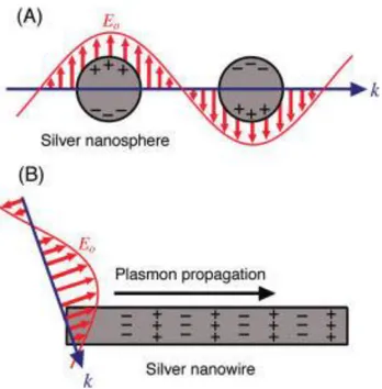
Figure 1.3 Schematic illustration of the two types of plasmonic nanostructures excited by the electric
field (E0) of incident light with wavevector (k). In (A) the size of nanostructure is smaller than the
wavelength of light and the free electrons can be displaced from the lattice of positive ions (consisting of nuclei and core electrons) and collectively oscillate in resonance with the light. This is known as a LSPR. In (B) the nanowire has one dimension much larger than the wavelength of light. In this case, light coupled to the nanostructure will excite the free electrons to create a PSP that can travel along the surface of the metal nanostructure. The schematic illustration was taken from reference [6].
Figure 1.4 (AD) TEM images of Ag nanocubes with edge lengths of 36, 58, 99, and 172 nm, respectively. In (E) the LSPR of the nanocubes red shifts as the edge length of the nanocubes increases. The graph was taken from reference [6].
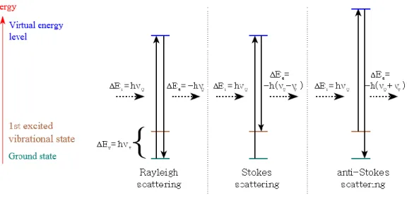
Figure 1.5 The different possibilities of visual light scattering: Rayleigh scattering (no exchange of
energy so the incident and emitted photons have the same energy), Stokes scattering (the atom or molecule absorbs energy and the emitted photon has less energy than the absorbed photon) and anti-Stokes scattering (the atom or molecule loses energy and the emitted photon has more energy than the
absorbed photon). The graph was taken from internet.
http://en.wikipedia.org/wiki/File:Ramanscattering.svg
Figure 1.6 Schematic of SERS. The SERS spectrum shown as an example was collected from 10-9 M adenine in a solution of silver nanoaggregates. The SERS signal PSERS depends on excitation intensity IL
and an effective SERS cross section = A(vL) 2
A(vS) 2
, which benefits from the EM enhancement described by field EFs A(vL) and A(vS) for the excitation and scattered field, and a chemical SERS effect,
described by an increased Raman cross section of the adsorbed molecule compared to the cross section in a ‘‘normal’’ Raman experiment . N is the number of molecules involved in the SERS process. The graph was taken from reference [45].
XI
Figure 1.7 Jablonski diagram. After an electron absorbs a high energy photon the system is excited
electronically and vibrational. The system relaxes vibrational, and eventually fluoresces at a longer
wavelength. The graph was taken from internet.
http://www.olympusmicro.com/primer/techniques/fluorescence/fluorescenceintro.html
Figure 1.8 Mechanisms of various light scattering processes. (a) Rayleigh, (b) nonresonance Raman, (c)
pre-resonance Raman, (d) resonance Raman resonance fluorescence (e) relaxed fluorescence. The graph was taken from the website of Horiba Scientific. http://www.azom.com/article.aspx?ArticleID=2950
Figure 1.9 Polyol method for synthesizing Ag nanostructures. In (A) the reduction of Ag ions by EG
leads to the formation of nuclei that are highly volatile. As the nuclei grow, fluctuations cease and their structure becomes static and contains multiply twinned boundary defects, singly twinned boundary defects, or are single crystalline with no boundary defects. These seeds are then grown into different nanostructures like (B) spheres, (C) cubes, (D) truncated cubes, (E) right bipryamids, (F) bars, (G) spheroids, (H) triangular plates, and (I) wires. The red lines in the illustration refer to a twin plane; the dark faces are {100}, and the light faces are {111}. The graph was taken from reference [6].
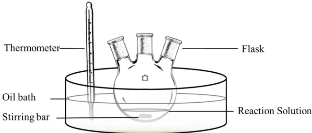
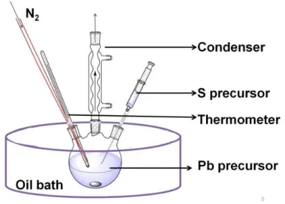
Figure 2.1 Schematic illustration of the setup for Ag nanostructures preparation. Figure 2.2 Schematic illustration of the air-free reaction setup for synthesizing QDs.
Figure 2.3 Schematic illustration of the synthesis of thin-shell PbS/CdS QDs by cation exchange.
Figure 2.4 Schematic illustration of EDX. The graph was taken from internet. http://commons.wikimedia.org/wiki/File:EDX-scheme.svg
Figure 2.5 The nanoscale spectroscopy of a silver nanowire (blue) and nanoslot (red) probed by EELS
(insert on the right). The graph was taken from reference [3].
Figure 2.6 a, Schematic illustration of the confocal Raman system. The optical path 1 is for the Raman
imaging, and the optical path 2 is for the measurement of Raman spectra. b, Sketches for Raman image and spectra acquisition. When using the image function, mirrors 1&4 are moved into the optical path, and the optical path 2 is thus blocked. The laser is focused on one end of the Ag wire through an objective, the Raman signals from the sample are collected by the same objective. After passing the Rayleigh filter, the optical signals go through an angle dependent narrow band pass filter, which permits one Raman peak (±20 cm-1) pass, and arrive at the TE air cooled 576×400 CCD to produce an image. To acquire remote Raman spectra, mirrors 1&4 should be moved out of the path, and the confocal Raman spectral acquisition mode marked with path 2 is then used for collecting Raman spectra with the same CCD. The top left, bottom left and bottom right mirrors need to be adjusted to move the laser focus point to the
XII
position for plasmon excitation, e.g. one end of the Ag nanowire. The graph was taken from reference [28].
XIII
LIST OF CHEMICAL COMPOUNDS, ABBREVIATIONS AND
SYMBOLS
Chemical compounds
AgNO3 silver nitrate
CdO cadmium oxide CF3COOAg silver trifluoroacetate
C6H8O6 ascorbic acid
HCl hydrochloride acid HNO3 nitric acid
NaSH sodium hydrosulfide PbCl2 lead (II) chloride
S sulfur
Abbreviations
ADF annular dark field
BEM boundary element method
EDS energy dispersive X-ray spectroscopy EELS electron energy-loss spectroscopy EG ethylene glycol
EM electromagnetic FCC face centered cubic
FDTD finite-difference time-domain FOM figure of merit
FP Fabry-Pérot
HRTEM high resolution transmission electron microscopy LSP(s) localized surface plasmon(s)
XIV LSPR localized surface plasmon resonance MGITC malachite green isothiocyanate NIR near-infrared NP(s) nanoparticle(s) OA oleic acid ODE octadecene OLA oleylamine 1D one dimensional PEG polyethylene glycol PL photoluminescence PMMA polymethylmethacrylate PSP(s) propagating surface plasmon(s) PVP poly(vinyl pyrrolidone)
QD(s) quantum dot(s) RIU refractive index unit
SAED selected area electron diffraction SEF surface enhanced fluorescence SEM scanning electron microscopy SERS surface enhanced Raman scattering SP(s) surface plasmon(s)
SPP surface plasmon polariton SPR surface plasmon resonance TEM transmission electron microscopy THF tetrahydrofuran
UV ultraviolet Vis visible
XV XRD X-ray diffraction
Symbols
absorption power
effective cross sections
effective cross sections of absorption effective cross sections of scattering E0 energy of a photon
A(vL) enhancement factors for the excitation field
A(vS) enhancement factors for the scattered field
ω frequency I incident intensity
Raman cross section scattering power
surface plasmon resonance sensitivity the wavelength
k wavevector
1
CHAPTER 1
INTRODUCTION
In human history, three nonradioactive members of Group 11 in the periodic table, copper (Cu), silver (Ag), and gold (Au) have played an important role since they are used to mint coins.[1] Coinage metals have shining appearance due to their excellent reflective properties for visible (Vis) light and intense color by coupling to light.[2] Their fascinating optical performance has drawn plentiful applications. Coinage metal nanoparticles (NPs) have been exploited by artisans since the days of the Roman Empire as colorants in cloths, stained glasses (Figure 1.1) and ceramics.[3, 4] Lycurgus cup [5] represents the outstanding achievement of the application of metal’s optical properties (Figure 1.2). The Lycurgus Cup is made by the Romans dating back to the fourth century. When viewed in reflected light (e.g., in daylight) it appears green, and when viewed in transmitted light (i.e., light is shone into the cup and transmitted through the glass), it appears red.[5] These typical cases are the applications of surface plasmon resonance (SPR) in ancient times. Today, the research of SPR has attracted much interest due to its ability of efficiently manipulating light on a deep sub-wavelength scale and its potential applications, which goes far beyond decorations.
Figure 1.1 Davos seaworth stained glass window. The graph was taken from internet. http://guad.deviantart.com/art/Davos-Seaworth-Stained-Glass-Window-330453541
The growing field of research on SPR has been focused on maneuvering the metal-light interactions, which is known as “plasmonics”.[2, 6, 7] In this branch of research, metal nanostructures serve as antennas to convert light into localized electric fields, as sensors to detect
2
the change of the local dielectric environment, and as wave guides to confine and route light below the classical diffraction limit. These properties can result in many applications, such as chemical and biochemical sensors,[8-10] surface enhanced spectroscopy for sensors,[11-13] photothermal therapy[12, 14, 15] and nanophotonic waveguides and so on.[16-18] All these applications strongly depend on the metal-light interactions. With precisely controlled size, shape, and/or spacing of nanostructures, light can be effectively manipulated and controlled with unprecedented accuracy.[14] The development of new methods make it is possible to realize this level of control.[19-22] Such exquisite synthetic control and advanced detection instruments in combination with powerful electromagnetic (EM) modeling tools have provided a better understanding of the metal-light interactions.[10] Of the metals, Ag has attracted interest in the research of plasmonics, and its advantageous properties have led to most applications in relevant fields.[6, 21, 23]
Figure 1.2 The Lycurgus Cup in reflected (left, green color) and transmitted (right, red color) light. Height: 16.5 cm (with modern metal mounts), diameter: 13.2 cm. © The Trustees of the British Museum. The graph was taken from internet. http://www.forumancientcoins.com/numiswiki/view.asp?key=cage%20cup
1.1
Plasmonics
In physics, a plasmon in metal is the quantized collective oscillation of conduction electrons excited by EM radiation.[18, 24, 25] In a classical picture, mobile free electrons repel each other and are attracted to the fixed positive ion cores in a metal. Under an external time-varying EM field, electrons will be forced to oscillate collectively against the restoring force of positive nulcei until the energy is lost as a result of resistance or damping. When the frequency of external EM field (light) is below the metal’s plasmon frequency, the electrons will screen the
3
electric fields of light and the light is reflected. On the contrary, when the incident frequency is above the metal’s plasmon frequency, the response of electrons could not be quick enough and the incident waves are transmitted instead.[2] The ability of a metal nanoparticle to support an SP is dependent on its dielectric function ε, which includes a real part (describing the strength of the polarization induced by an external electric field) and an imaginary part (describing the loss encountered in polarizing the material). Both factors vary with excitation wavelength (λ). Thus, a small value of imaginary part is important to minimize the loss. To achieve the resonance condition, a negative real part of dielectric constant is necessary, which is not possible for standard dielectrics and nonmetals that typically have positive values. At the same time, the imaginary dielectric constant should be close to zero to support a strong resonance. The performance of the plasmon in a metal, which has a negative real and small positive imaginary dielectric constant, can be quite pronounced because its plasma frequency generally falls in the visible (Vis) spectral range and it has a high electrical conductivity. Among the metallic elements, silver has the best performances at optical frequencies with lowest energy loss. Gold is often the choice at lower frequencies, having the advantage of being chemically stable in many environments. However, the interband losses of gold in the Vis spectrum (< 500 nm) are high. Similarly, copper is plagued by large interband losses over most of the Vis spectrum. Thus, silver and gold have predominately been the choice for plasmonic applications.[2, 26]
Bulk (or volume) plasmons are the quantized bulk oscillations of electrons.[2] The frequency is defined as[2]
(1)
where is the electron density, is the electron charge, is the relative permittivity of free space and is the electron mass. It is must be noted that the bulk here refers to a material with all three dimensions much larger than the wavelength of light.[9] Surface plasmons (SPs) are those tightly bound to the metal-dielectric interface.[9] They have lower energy than bulk (or volume) plasmons and can couple with photons to result in a quasi-particle called a surface plasmon polariton (SPP).[10]
Two types of plasmonic modes exist: (i) nonpropagating localized surface plasmons (LSPs) and (ii) propagating surface plasmons (PSPs).[2, 6] LSPs are supported by nanostructures with a size
4
smaller than or comparable with the excitation wavelength in three dimensions, as shown in Figure 1.3A. In this case, the structures experience a nearly uniform EM field associated with the light (E0).[6] Two effects are important for LSPs. First, LSPs, once excited, have the striking ability to squeeze light into nanometer dimensions, producing the large local enhancement of EM energy. The EM field reaches its maximum at the interface, and exponentially decays away from the surface. Second, the LSPs can be excited when the excitation frequency (ω) matches their natural frequency, and strong resonance occurs, commonly known as localized surface plasmon resonance (LSPR). LSPR results in strong light scattering, intense absorption and the maximum enhancement of the local EM field.[9] The frequency and intensity of LSPR depend on the composition, size, and shape of nanostructures and their dielectric environments.
Figure 1.3 Schematic illustration of the two types of plasmonic nanostructures excited by the electric field (E0) of incident light with wavevector (k). In (A) the size of nanostructure is smaller than the wavelength of light and the free electrons can be displaced from the lattice of positive ions (consisting of nuclei and core electrons) and collectively oscillate in resonance with the light. This is known as a LSPR. In (B) the nanowire has one dimension much larger than the wavelength of light. In this case, light coupled to the nanostructure will excite the free electrons to create a PSP that can travel along the surface of the metal nanostructure. The schematic illustration was taken from reference [6].
PSPs are supported by structures with one or two dimensions larger than the wavelength of incident light, as described in Figure 1.3B. They can travel along the metal surface up to hundreds of micrometers.[10] The associated EM field also decays exponentially from the
5
interface. In particular, in one dimensional (1D) nanostructures, SPs could be excited and propagate back and forth between two ends, behaving like Fabry-Pérot (FP) resonators.[6, 27] By controlling the morphology of the structure, the propagation distance (tens of micrometers in nanowires) and the PSP waves can be manipulated.[6, 28] The investigation of light-metal interactions is known as “plasmonics”, which is related to the localization, guiding, and manipulation of EM waves beyond the diffraction limit and down to the nanometer-length scale.[6, 18, 24, 26] The extraordinary advances in fabrication (such as electron-beam lithography, wet-chemical synthesis and focused ion-beam milling), characterization of metal nanostructures, (such as scanning electron microscopy (SEM), dark-field and near-field optical microscopies) and the emergence of EM simulation tools (based on Mie theory, discrete dipole approximation, boundary element method (BEM) and finite-difference time-domain (FDTD) methods) allowed the rapid development of the field of plasmonics.[24, 26]
1.2
Plasmonics in Nanostructures
The LSPR of metal nanostructures is attributed to the collective oscillation of electrons.[14, 29, 30] When light interacts with metal nanostructures, LSPR is excited and the incident light is dissipated in the form of heat within the nanostructures, which results in strong absorption or reradiated into free space which is scattering.[26] To understand in depth how the metal-light interact, which strongly depends on the particle geometry and dielectric environment, we must turn to theory. Basically, effective cross section () has been used to describe the absorbed or scattered power. of absorption ( ) and scattering( ) is defined as the ratio of the absorption ( ) and scattering ( ) power (photons s1) to the incident intensity (I, photons s1 cm2), respectively, as described below:[26]
(2)
(3)
The extinction cross section is thus defined as:
6
When the LSPRs happen, the extinction cross section could be increased by several times.
The size and shape of nanostructures have a critical effect on the plasmonic features, such as frequency, bandwidth and intensity of LSPR.[31] The size of a nanoparticle determines plasmonic features that include the ratio of absorption to scattering, the number of LSPR modes, the peak position of an LSPR mode, and the extent of PSP localization.[6] For small spherical nanoparticles, they generally exhibit one dipole mode when their radius R is much smaller than the wavelength of light. The and are directly proportional to R3 and R6, respectively. When R is smaller than ∼30 nm, the LSPR extinction is dominated by absorption.[2, 27, 32] When the size of particles increases, they will scatter light more efficiently.[17] At the same time, the peak position of LSPR will red shift and the width will broaden due to the larger charge separation. Higher order modes will appear as well. In another case, as shown in Figure 1.4, with the increase of the silver nanocube size, the peak position of LSPR shifts to red accompanied by the broadening of the peak.
Figure 1.4 (AD) Transmission electron microscopy (TEM) images of Ag nanocubes with edge lengths of 36, 58, 99, and 172 nm, respectively. In (E) the LSPR of the nanocubes red shifts as the edge length of the nanocubes increases. The graph was taken from reference [6].
Shape is another critical parameter for plasmonic features.[33] When the symmetry of a structure decreases, the number of resonances increases because the electrons could be polarized in more ways. At the same time, the dipole mode is lower due to lacking centrosymmetry. With the appearance of sharp corners, the LSPR peaks redshift due to a greater charge separation. Via different synthesis approaches, Ag nanostructures of different shapes, such as nanospheres,
7
nanocubes, nanorice structures and nanowires, have been achieved.[23] The spherical Ag NPs in general only show one SPR peak, but in a big contrast, 1D structures, such as nanobars and nanorice structures, support both transverse and longitudinal resonances, with the latter tunable from the Vis to near-infrared (NIR) spectral range by controlling the aspect ratio (length/diameter) and/or length.[15, 34] In addition, with increasing aspect ratio, higher order multipolar SPR modes, which behave like FP resonators, can be excited.[27, 35-37]
Tailoring the size and shape of metal NPs allows the tuning of the SPR to a desired frequency, and also offers the opportunity to achieve the highest possible enhancement of the EM field. For example, sharp surface curvatures and tips (in prisms[8]or rods [38]) as well as junctions (in core/shell structures[39] or dimers[8]) can yield a large EM enhancement. In the last two decades, the development of nanofabrication techniques allows the manipulation of NP geometries and assemblies.
1.3
Plasmonic Applications
Up to now, numerous applications based on plasmonics have emerged, which can be categorized into three thrusts: (i) taking advantage of the nanostructures’ ability as antennas to concentrate light into localized electric fields to enhance or modify the optical features of nearby reporters, such as surface enhanced spectroscopy for sensor applications;[40, 41] (ii) exploiting the sensitivity of nanostructures’ LSPR properties toward their local dielectric environments to detect the change on the metal surface or of surroundings for applications, such as LSPR-based chemical and biochemical sensing and detection;[10, 14, 42] (iii) acting as waveguides to confine and route light with plasmonic circuitry.[24, 43, 44] Herein, some typical applications in the thrusts mentioned above are discussed in the following section.
1.3.1 Surface Enhanced Raman Scattering
Raman scattering is inelastic scattering of light as a result of its interaction with matter.[45, 46] Raman spectroscopy is used as a powerful tool for chemical analysis, which gives spectral fingerprints, characteristic of Raman active molecules and it is sensitive to composition, bond strength, environment, and structure. Although the inelastic scattering of light was predicted by Adolf Smekal in 1923, it was not observed in experiment by Sir Chandrasekhara Venkata Raman
8
and Kariamanickam Srinivasa Krishnan until 1928, and was then named as Raman effect.[13] For the spontaneous Raman effect, a photon excites the molecule from the ground state to a virtual energy state. When the molecule relaxes, it emits a photon and returns to a different rotational or vibrational state. The difference in energy between the original state and this new state leads to a shift in the emitted photon’s frequency away from the excitation wavelength (Figure 1.5). The Raman scattering intensity is determined by excitation intensity and the Raman cross section . depends on the polarizability derivative of the molecular vibration.[45] In most cases, the number of inelastically scattered photons is extremely small, due to rather low Raman scattering cross sections ( ) of 10-3010-25 cm2 per molecule, although higher values may be obtained under resonance conditions.[10, 45] The small Raman cross sections require a larger number of molecules to be involved for detection. As a consequence, the use of Raman spectroscopy in ultrasensitive trace detection is limited.
Figure 1.5 The different possibilities of visual light scattering: Rayleigh scattering (no exchange of energy so the incident and emitted photons have the same energy), Stokes scattering (the atom or molecule absorbs energy and the emitted photon has less energy than the absorbed photon) and anti-Stokes scattering (the atom or molecule loses energy and the emitted photon has more energy than the absorbed photon). The graph was taken from internet. http://en.wikipedia.org/wiki/File:Ramanscattering.svg
In 1970s, Jeanmaire, Van Duyne, Albrecht and Creighton independently observed that adsorption of pyridine onto electrochemically roughened Ag surfaces could increase the Raman scattering intensity by a factor of ~106.[7, 13, 47, 48] This striking discovery was denoted the surface enhanced Raman scattering (SERS) effect (Figure 1.6). SERS effect can handle the
9
problem mentioned before; however, its widespread application was limited by obstacles such as the irreproducibility of substrates. The development of nano-fabrication techniques have significantly contributed to obtaining reliable, reproducible and highly-sensitive SERS substrates. As a result, there has been a renewed interest in Raman spectroscopy as exciting advances of the past 1015 years.[7, 19, 40, 49] Using metal nanostructures, SERS intensities could reach the single-molecule detection level with enhancement factors (EFs) up to 1015.[11, 47]
Several theories have been developed to explain the origin of SERS, with “EM field enhancement”[24, 50] and “chemical enhancement”[51] being generally accepted ones. In EM field theory, an amplified EM field can give rise to EFs of 10101011.[24, 50] This effect is provided by SPs transferring energy to the analytes through focusing light to generate the enhanced EM field. When the incident light strikes the surface, localized SPs are excited. The field enhancement is greatest at resonance. In order for scattering to occur, the plasmon oscillations must be perpendicular to the surface because scattering will not take place with in-plane oscillations. Because of this requirement, roughened surfaces or arrangements of nanostructures are typically required. The SERS effect can be quite pronounced because the field enhancement occurs twice. Firstly, the field enhances the incident light and secondly, the field enhances the Raman scattering, resulting in further increase in the total output. At each stage the electric field is enhanced as E2, for a total enhancement of E4.[45] The enhancement is not equal for all frequencies. When the frequency shift between Raman signal and the incident light is small as compared to the width of the SPR, both the incident light and the Raman signal can be at resonance with the plasmons, leading to the E4 enhancement with A(vL) A(vS)). When the
frequency shift is large, the incident light and the Raman scattering cannot both be on resonance, thus the enhancement cannot be maximal. For this reason, Au, Ag and Cu are considered as best metals for SERS because their SPR falls in the Vis and NIR range.[45] The second and less prominent mechanism is the “chemical enhancement” or “electronic enhancement”, [51] which arises from metal-molecule interactions. Metal-molecule charge transfer can take place, which modifies the electronic states of molecules and alter their Raman cross section, leading to more efficient Raman scattering.[45] This type of enhancement is sensitive to the surface properties of SERS substrates and the nature of analyte molecules. It is thought to be responsible for at most two orders of magnitude of the enhancement. The large of contribution from the EM field enhancement has made it a preferred route for SERS investigations. Therefore, choice of SERS
10
substrates and excitation wavelength are critical factors for observing maximal Raman enhancement.
Figure 1.6 Schematic of SERS. The SERS spectrum shown as an example was collected from 10-9 M adenine in a solution of silver nanoaggregates. The SERS signal PSERS depends on excitation
intensity IL and an effective SERS cross section = A(vL)2A(vS)2, which benefits
from the EM enhancement described by field EFs A(vL) and A(vS) for the excitation and
scattered field, and a chemical SERS effect, described by an increased Raman cross section of the adsorbed molecule compared to the cross section in a ‘‘normal’’ Raman experiment . N is the number of molecules involved in the SERS process. The graph was taken from reference [45].
SERS is typically used for capturing and identifying specific signal for ultrasensitive detection of unknown species and for imaging by creating SERS “tags”. For example, flower-like silver mesoparticles with highly roughened surfaces were used as SERS substrates.[52] The structures were functionalized with dye molecules, and high and reproducible SERS enhancements in the order of 107–108 on average could be achieved. As a result, the detection limitation could reach the single molecule level. In another case, silver NPs were functionalized with dye molecules as SERS tags for in vivo cancer imaging.[53] The excitation wavelength was chosen in the NIR range, and then the penetration depth reached up to a few centimeters. By this method, small tumors could be identified and located noninvasively using a Raman system.
1.3.2 Surface Enhanced Fluorescence
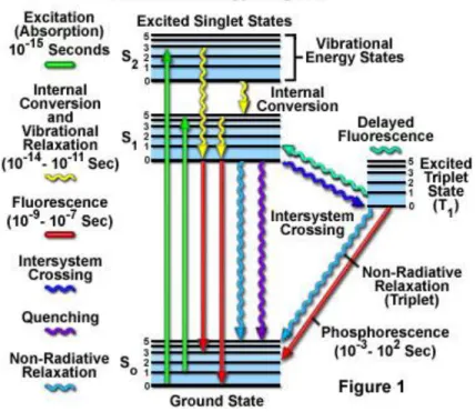
Fluorescence is the emission of light by matter induced by absorption of EM radiation (Figure 1.7).[54] The wavelength of emission is generally longer than the absorbed radiation wavelength.
11
In some special cases, a pair of photons with same or different energy could be absorbed by one electron when the incident EM radiation is intense; this can lead to emission of a shorter wavelength, which is called “two-photon absorption”.[55] The wavelength of emission may also be the same as that of the absorbed radiation, termed "resonance fluorescence".
Fluorescence emission and Raman scattering are two different and competing phenomena, with the major differences being the nature of intermediate states and the time scale involved in these processes (Figure 1.8). As mentioned in previous sections, in the Raman scattering, generally virtual states are involved, while in fluorescence real states are concerned. The existence of such virtual states explains why in Raman scattering, the interaction of the photon with the molecule and the re-emission of scattered photon occur almost simultaneously (10-12 s, picosecond), while the lifetime in fluorescence is longer (10-9 s, nanosecond).
Figure 1.7 Jablonski diagram. After an electron absorbs a high energy photon the system is excited electronically and vibrationally. The system relaxes vibrationally, and eventually fluoresces at a longer wavelength. The graph was taken from internet. http://www.olympusmicro.com/primer/techniques/fluorescence/fluorescenceintro.html
When the energy of excitation photon gets close to the transition energy between two electronic states, resonance Raman or resonance fluorescence will happen. In contrast with resonant fluorescence, relaxed fluorescence is the emission of a photon from the lowest vibrational level
12
of an excited electronic state. When the excitation energy is lower, fluorescence could not take place and only off-resonance Raman scattering could be excited. However, in resonance excitation, the fluorescence is much more intense than Raman scattering and general hiding Raman features, because the fluorescence scattering cross section is 10171016 cm2 per molecule, much larger than that of Raman 10-3010-25 cm2 per molecule.[45] For this reason, when searching for the more informative Raman spectrum, the fluorescence should be avoided, for example, select the longer excitation wavelength.
Figure 1.8 Mechanisms of various light scattering processes. (a) Rayleigh, (b) nonresonance Raman, (c) pre-resonance Raman, (d) resonance Raman resonance fluorescence (e) relaxed fluorescence. The graph was taken from the website of Horiba Scientific. http://www.azom.com/article.aspx?ArticleID=2950
Ultraviolet (UV)-excited fluorescence in the Vis region has led to many practical applications including photodetectors, fluorescent labeling, dyes, light-emitting diodes, biosensors and solar cells.[56-58] Although fluorescence has relatively large cross sections, there is still a driving force for faster detection, enhanced intensity and higher signal-to-noise ratios. Recently, metallic nanostructures were used to modify the spectral properties of fluorophores and to alleviate some of these photophysical constraints.[59-63] When fluorophores are located in the vicinity of metallic nanostructures, the photoluminescence (PL) could be enhanced. It is called surface enhanced fluorescence (SEF).[26, 64-67] SEF occurs due to fluorophores’ interaction with metallic nanostructures, which result in modifications of their excitation/emission activities.[41, 57, 68-70] The strength of these interactions depends on the overlap degree of SPR with the absorption/emission of fluorophores, and the distance between metal and fluorophores.[71, 72]
13
The plasmon/fluorophore interactions lead to three effects: excitation enhancement (amplified excitation light that leads to an enhanced absorption), emission enhancement (increased radiative decay thus an amplification of emission) and quenching (increased nonradiative decay).[58, 66, 70, 72, 73] In general, for the excitation enhancement mechanism, the PL intensity is directly proportional to the EM field enhancement E2.[6, 73] For the emission enhancement mechanism, radiative rate could be increased and thereby the lifetime and quantum yield are modified. Quenching occurs when the distance between metal and fluorophores is smaller than ~5 nm, so the coupling distances should be controlled at 5 nm.[33, 74] Overall, the final performance is determined by the competition between enhancement and quenching effects. EFs vary from 2 to 100, which depend on the particular plasmon/fluorophore system.[6, 69] SEF can be used to increase detection sensitivity. For example, colloidal semiconductor quantum dots (QDs) were assembled between layers of metal NPs to create a highly strong plasmon-exciton interaction in the plasmonic cavity.[75] In such a plasmon/fluorophore system, Ozel, et al observed an EF of 4.4 and a shortened decay lifetime. Such strong plasmon-exciton coupling nanocomposites hold great promise for future exploitation and development of QD plasmonic biophotonics and QD plasmonic optoelectronics.[75]
1.3.3 Optical Detection of the Change in Refractive Index
Optical properties have been largely exploited for biological labeling and diagnostic applications.[76, 77] One of the simplest applications in this branch is to detect the change of environmental refractive index through measuring the shift of SPR peak location, which is quite sensitive to the variation of the refractive index of the local environments.[7, 9, 10, 78]. When refractive index changes, the wavelength of SPR peak shifts follow an approximately linear relationship. The SPR sensitivity ( ) is reported as nanometers of peak shift ( ) per refractive index unit (nm RIU-1). [9, 79]
(5) The sensitivity achieves the highest value at the wavelength and the angle of incident light, which could satisfy the resonance condition. In general, nanostructures are first dispersed in solution directly or immobilized on glass substrates and inserted into solution later, and then the
14
extinction or scattering spectra are measured. By monitoring the peak shift, the variation of the refractive index of the solution could be measured. The precision of the sensitivity is described as a figure of merit (FOM) which is defined by the sensitivity and the resonance line width.[9]
(6) Many noble metal nanostructures, such as gold nanorods in solution,[42] silver nanorice structures immobilized on glass slips[80] or dispersed in solution[35, 81], nanoholes and nanohole arrays,[10] have been used for this purpose. The size, shape, composition, and inter-particle spacing could affect the detection sensitivity.[8] For example, when the end curvature, the aspect ratio of 1D nanostructures and the size uniformity increase, the SPR sensitivity increases.[42, 81] In addition, the capping agents, which have been used during the synthesis process also play an important role in this application. When the surface of nanostructures is functionalized with capture molecules, target molecules can be detected as their binding with capture molecules alters the dielectric environment near of the surface that can be monitored by the shift of SPR.[6]
1.4
Synthesis of Silver Nanostructures
1.4.1 Unique Properties of Silver Nanostructures
Nobel metals offer many advantages for plasmonic applications with respect to other plasmonic metals.[82] First, the frequency of SPRs is at the desired region, i.e., the Vis to NIR range. If the excitation frequency is lower than that of metal’s SPR, the light will be reflected. Unlike most metals, whose SPR frequency is in the UV range and are shiny in the Vis range, noble metal such as Au,[15] Ag,[6, 33] and Cu,[83] yield strong SPR in the Vis-NIR region, resulting in strong absorption and showing special colors. In particular, silver is able to exhibit a strong SPR tunable over a wavelength range of 300 to 1200 nm, wider than that of most plasmonic metals.[6] In addition, comparing with gold, silver has sharper resonances, higher refractive index sensitivity, and is less dissipative.[16, 23, 84] More importantly, silver is also a good candidate for SPP applications with respect to other metals, such as Au and Al, because it possesses the lowest absorption in the Vis region with typical SPP propagation distance ranging from 10-100 μm at a
15
Ag/air interface. Moreover, the chemical stability of silver can be improved by forming a silver sulfide thin film on the surface to prevent oxidation.[6]
1.4.2 Synthesis of Silver Nanostructures
The size and shape of nanostructures have a critical effect on the frequency, bandwidth and intensity of LSPR.[17, 33] The ability to control such physical parameters of silver nanostructures and further to maneuver their plasmonic properties are important for practical application. A lot of investigations have been focused on the size-controlled[85] and shape-controlled[86] wet chemical synthesis of silver nanostructures in the last two decades, and the development of nanofabrication techniques allow the manipulation of nanostructure geometries and assemblies using another approach. Wet chemical procedures involve the reduction of metal precursors to metal atoms, and the controlled aggregation of atoms into nanostructures. In general, the wet-chemistry approach, such as the citrate reduction method, polyol method, has proved to be a reproducible, high-yield, large-scale synthesis method to obtain Ag nanostructures with excellent optical properties.[23] As shown in Table 1.1, many silver nanostructures could be obtained from wet chemical methods. For example, the size of silver nanocubes was tuned from 30-70 nm by introducing a trace amount of sulfide or hydrosulfide into reaction solution and by switching silver precursors.[87] It was further tailored in the range of 18-32 nm by quenching the reaction at different times.[88] In addition to the size control, the geometry of silver nanostructures could also be adjusted.[21] Shapes like spheres,[23, 89] cubes,[87] icosahedra,[90] triangular nanoprisms,[91] bars,[92] nanorice structures,[92, 93] rods[94] and wires[16] could all be synthesized by wet chemical methods. In the following, we focused our brief discussion on several wet chemical methods.
Citrate reduction is a popular method for quickly synthesizing silver colloids, which was first reported in 1982.[95] In this method, AgNO3 is used as a precursor and citrate is used as both reducing agent and a stabilizer. Silver NPs could be obtained by adding certain amounts of aqueous sodium citrate solution into silver nitrate aqueous solution under boiling. This method is feasible but it is hard to control the shape and size.[96, 97] A large variety of sizes and a diversity of shapes of the products make fundamental studies rather complicated and also limit their practical applications.
16
Table 1.1 Summary of the Shapes, LSPR Absorption Peaks, Demonstrated Applications, and Methods for the Synthesis of Ag Nanostructures
a
The main absorption peak (nm).b Assembly means the nanostructure has been assembled into larger structures for plasmonic applications or studies. The red lines in the illustration refer to a crystalline plane; the dark faces are {100}, and the light faces are {111}. The table was taken from reference [6].
The silver mirror reaction is a chemical deposition method used to form Ag coating on various types of substrates.[98] In this approach, AgNO3 is used as a precursor to form the Tollen’s reagent, a sugar or an aldehyde-containing compound is used as reducing agent to generate elemental Ag. The silver mirror reaction could generate a shiny coating made of small
17
particles,[99] leaf or flowerlike fractal structures[98] of Ag on objects, but no shape control has been reported with this technique.
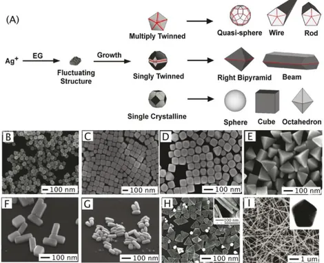
Polyol process that has been widely used in the controlled synthesis of silver nanostructures is a robust and versatile method.[6] Polyols are compounds with multiple hydroxyl functional groups available for reactions. By varying reaction conditions, such as reaction temperature, reaction time, capping agent, reagent concentration and trace ions, the nucleation and further growth process could be highly controlled to obtain nanostructures with different morphology and size.[20, 100] A number of morphologies synthesized through this method are listed in Table 1.1 and further shown in Figure 1.9.
Figure 1.9 Polyol method for synthesizing Ag nanostructures. In (A) the reduction of Agions by EG leads to the formation of nuclei that are highly volatile. As the nuclei grow, fluctuations cease and their structure becomes static and contains multiply twinned boundary defects, singly twinned boundary defects, or are single crystalline with no boundary defects. These seeds are then grown into different nanostructures like (B) spheres, (C) cubes, (D) truncated cubes, (E) right bipryamids, (F) bars, (G) spheroids, (H) triangular plates, and (I) wires. The red lines in the illustration refer to a twin plane; the dark faces are {100}, and the light faces are {111}. The graph was taken from reference [6].
In polyol method, AgNO3 or CF3COOAg are used as precursors, with the first one being more commonly used. However, CF3COOAg-invovled synthesis has some unique features that could be beneficial for the preparation of certain structures, such as a lower reaction temperature,
18
higher stability, and insensitivity to trace impurities. Polyol reagents, such as ethylene glycol (EG), polyethylene glycol (PEG), 1,2-propylene glycol, or 1,5-pentanediol can serve as both solvents and reducing agents.[23] The reduction happens when Ag precursors and capping agents are mixed in the presence of polyols, especially at an elevated temperature. The capping agents are generally used to stable the particle and play a role as shape control through selectively binding the facets of nanocrystal. At the beginning, silver ions are reduced as atoms to form small clusters of fluctuating structures. With the reaction continuing, the clusters grow larger and form more stable structures, such as single crystalline, singly twinned and multiply twinned nanocrystals, which then act as seeds. The seeds with different inner structures ultimately develop into the nanostructures of different morphologies.[6]
1.5
Thesis Objectives and Organization
1.5.1 Our Objectives Part I: Synthesis
Although some Ag nanostructures have been synthesized with tunable size and shape as mentioned above, it is challenging to synthesize uniform Ag nanorice structures with high reproducibility. The growth mechanism of such nanostructures is not well understood and the knowledge on key shape determining parameters also remains limited. The ability to understand these aspects can potentially lead to better control over the reproducibility, shape uniformity, and yield on the shape-directed synthesis of these nanorice structures. In addition, their optical properties require further investigation before they can be explored for practical applications. Moreover, although some 1D Ag nanostructures have been fabricated from solution, nearly all of them are highly symmetric. This feature is attributed to the crystal symmetry in face centered cubic (FCC) structure, which inhibits asymmetric growth.[22] Rare examples of asymmetric 1D nanostructures have been reported, such as Cu nanobats,[83] rod-needle and plate-belt Ag hetero-nanostructures[101] and tadpole-shaped Au nanowires.[102] However, a detailed analysis of the plasmonic properties of these asymmetric nanostructures is lacking. The controlled preparation of asymmetric silver nanostructures with well-defined SPR peaks using a simple solution synthesis method is thus desirable for creating novel platforms for exploring morphology-dependent optical properties, but remains a significant challenge. Given these gaps
19
in synthesis and understanding, in the Part I, we further investigated the growth process of the silver nanorice and nanocarrot structures.[103] The optical properties of these silver nanostructures were further examined. The objectives for Part I are:
1. Studying the growth mechanism of silver nanorice structures. By understanding the growth mechanism, further optimizing and gaining more control over the synthesis to achieve adjustable silver nanostructures by changing the reaction parameters.
2. Synthesizing novel asymmetric silver nanocarrot structures and corresponding structure/property relationship characterization. In addition, the growth mechanism will be investigated.
3. Analyzing the plasmonic properties of both structures in detail by optical extinction spectroscopy and electron energy-loss spectroscopy (EELS).
4. Measuring the sensitivity of both structures to the refractive index of their environments.
Part II: Investigation of Potential Applications
Surface enhanced spectroscopy (such as SERS and SEF) is one of these popular plasmonic applications of silver nanostructures. For these applications, the substrates and excitation wavelength are critical factors that influence the observed enhancement. Vis and NIR radiations are usually used to excite SPR modes of silver nanostructures to provide maximal enhancement. As for metal substrates, the EM field intensity distribution around them is not uniform and depends strongly on their morphology. Structures with sharp surface curvatures and tips[52] (in prisms[8]or rods [38]) and junctions[104] (in core/shell structures[39] or dimers[8]) can produce large EM enhancement. Further to achieve the strong coupling between plasmons of adjacent nanostructures, the distance below several nanometers is desired, but hard to control. Such gaps or junctions usually rely on the random assembly of small particles. Although a number of researches have focused on the applications based on the concept of surface enhanced spectroscopy, the production of reliable, reproducible, and highly sensitive substrates for sensing applications has been a big challenge.
Individual flower-like silver mesoparticles with rough surface have excellent performance in SERS.[52] The SERS EFs of dimers were 10-100 times larger than that of individual particles, which were further confirmed by our experiments. Such increases in SERS could arise from the
20
additional field enhancement in the interparticle gaps. The study of the enhancement mechanism and manipulation of the formation of dimers is necessary for SERS applications.[105]
SEF of colloidal QDs has drawn plentiful attentions recently. Among all kinds of QDs, lead chalcogenide QDs have both large excitation Bohr radii and small bulk band gaps, thus allowing quantum confinement in relatively large sized QDs simultaneously with a tunable NIR emission.[56, 57, 106] The intricate behaviour of plasmon/fluorophore interaction require extensive investigations to understand and control the relative contributions of the light absorption enhancement and alterations of both radiative and nonradiative decay rates, all these being crucial for the advancement of theoretical investigations and for practical applications. We focused on the PL enhancement in the plasmon/fluorophore system consisting of lead chalcogenide QDs and Ag NP film to investigate the interaction between QDs and plasmonic structures. Ag NPs instead of Ag “nanorice” or “naoncarrot” structures were used here because the high stability of NPs makes it easier to claim the concept for completing the preliminary work.
Therefore, the objectives for Part II are:
1. Investigating the incident polarization-dependent SERS of flower-like silver mesoparticle dimers and manipulating individual particles to form or break the dimers in order to investigate the enhancement mechanism in situ.
2. Fabricating coupled plasmon/fluorophore system consisting of lead chalcogenide QDs and Ag NP film and investigating the PL enhancement. By controlling the range of spectral superposition between the absorption/emission spectra of the QDs and the SPR of the Ag films, the enhancement mechanism will be studied.
1.5.2 Organization of the Thesis
This thesis is divided into four chapters and organized as follows:
Chapter 1 Introduction: introducing the background, motivation and objectives of this thesis. Chapter 2 Experimental, Characterization and Theoretical Modeling: describing experiment
details of synthesis processes of all kinds of silver nanostructures and QDs involved in the current study, investigating the potential applications in refractive index sensitivity and surface
21
enhance spectroscopy and introducing the main characterization techniques and the theoretical modeling methods.
Chapter 3 Results: Part I: Synthesis
Section I: Silver Nanorice Structures: Oriented Attachment-Dominated Growth, High Environmental Sensitivity, and Real-Space Visualization of Multipolar Resonances
Section II: Asymmetric Silver “Nanocarrot” Structures: Solution Synthesis and their Asymmetric Plasmonic Resonances
Part II: Investigation of Potential Applications
Section III: Enormous Surface Enhanced Raman Scattering from Dimers of Flower-like Silver Mesoparticle
Section IV: Photoluminescence Enhancement of Near-infrared Emitting PbS and PbS/CdS Core/shell Quantum Dots Induced by Silver Nanoparticle Film
Chapter 4 Conclusions and Perspectives: Concluding the main results and perspecting some
potential investigations in future work.
Most of work in this thesis was done by Hongyan Liang, however, some parts were conducted through collaboration. More specifically, the EELS measurements and corresponding calculations were performed by Dr. David Rossouw working in our collaborator Prof. Gianluigi A. Botton’s group. All QDs used in this thesis were provided by Dr. Haiguang Zhao, who also assisted with me for PL intensity and lifetime measurements. All Mie calculations were modeled by Prof. Zhipeng Li. The FDTD modeling was performed by Dr. Scott K. Cushing in our collaborator Prof. Wu’s group.