A VERSATILE LOW-COST AUTOMATION SYSTEM FOR AN
ELECTRO-IONIZATION EXPERIMENT
CH. SERVAIS, R. LOCHT and J. MOMIGNY
Département de Chimie Générale et de Chimie Physique, Université de Liège, Institut de Chimie, Sart-Tilman par B-4000 Liège 1 (Belgium)
ABSTRACT
A cheap complete automation system designed for an electro-ionization experiment is described. This system is based on a Sinclair ZX Spectrum computer and a modular architecture. The control program and general building blocks diagrams are discussed and give a general idea of how to build modules or procedures adapted to different applications.
INTRODUCTION
This paper describes the automation of an electro-ionization experimental set-up. For 15 years and until these recent changes, all the controls were operated manually. Computers were introduced a few years ago for recording, spectra treatment, and plotting purposes only. Recently, with the revolution in electronics and computer products, it has become possible to realize a low-cost, complete automation of the main controls, providing much more efficient use of an apparatus needing even less attention. Long periods during which the experiment is left on its own can now be fully exploited not only for long time measurements but also for numerous short spectra and automatic reference spectra recording. The spectral data and instrument settings are temporarily stored on a disc-like medium to be transferred later on to the main computer. A hard copy of these settings is also printed at the end of each recording. The architecture of the system is modular and could easily be modified to fit a particular application. Different computer-based acquisition systems have been described [1-3] and are built around IBM PC, LSI 11-2, or LSI 11-23 computers. In our case, a Sinclair Spectrum microcomputer with Sinclair interface 1 and microdrives was used as the central processing unit and the custom realized-modules provide examples of what can be built around such a cheap system. The currently used exploitation and acquisition program is described briefly at the end of this paper.
EXPERIMENTAL
The electro-ionization experiment before the installation of the automated control will be described briefly here to show the main features used in the exploitation of the system. A complete description can be found in ref. 4.
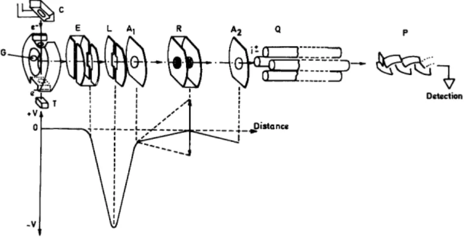
Fig. 1. Detail of the ion source and retarding lens. C, Cathode; G, gas inlet; T, electron trap; E, extraction lens; L, focussing lens; R, retarding lens; Al, A2, ion accelerating lenses; Q, quadrupole mass spectrometer; P, electron multiplier. The lower diagram gives the potential applied to the plates along the ion beam path.
Basically, electrons are emitted from a heated cathode, C, and accelerated by a potential which determines the electron energy (Fig. 1). These electrons are focused in an ionization chamber by permanent magnets. The electron beam is collected on the opposite side of the chamber by an electron trap, T, for cathode current monitoring. The ions produced by the interaction of molecules and electrons in the ion chamber are allowed to drift out of the chamber, extracted by lens E, focused by lens L, and accelerated by Al and A2. After kinetic energy analysis by a double retarding grid system, R, the remaining ions are finally mass-selected by a quadrupole mass spectrometer, Q, and accelerated on the cathode of an electron multiplier, P. The electron current is converted into a voltage and amplified by an electrometer. The signal, or its first derivative, is fed into a multichannel analyzer.
The complete operating conditions of the system are determined by (a) the electron accelerating potential;
(b) the electron beam current (determined by the heating intensity and wehnelt voltage); (c) the extraction and focus electrodes, E and L;
(d) the acceleration potential on Al and A2; (e) the retarding potential, R;
(f) the ion mass selection control; and
(g) the electron multiplier gain (determined by supply voltage)
Two kinds of data can be recorded; ionization efficiency curves and ion kinetic energy distribution curves. The ion current can be continuously scanned either with respect to the retarding potential at fixed electron energy or with respect to the electron energy at fixed retarding potential. Both signals can be electronically differentiated.
A slow ramp generator was used initially to create the varying voltages on C and R and send scan start pulses to a NS-560 multichannel analyzer [6]. Spectral data were transfered to a TN-4000 computer [6] through a 110 baud RS232 serial link.
GLOBAL SYSTEM DESCRIPTION
Automation can usually be thought of in terms of remote programming. The need to program the main controls of the experiment from a digital device was the main problem to solve. Two possibilities were envisaged: the first, and less satisfying, solution was the adaptation of small interfaces between the various controls and the computer. It has been rejected for two reasons.
(1) Due to the many different reference potentials of these controls, optically coupled interfaces should be used.
(2) The old multichannel analyzer and sweep generators would still have to be used and their old design would not allow for much programming flexibility.
The second solution was to emulate the functions of a modern multichannel analyzer and sweeper with a limited hardware housed in a few modules. The only really interfaced control was the quadrupole mass spectrometer mass control as it was obviously not reasonable to emulate such a device.
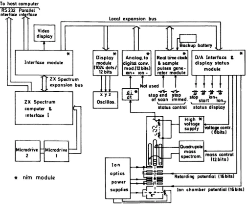
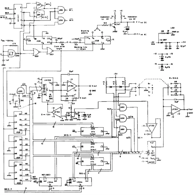
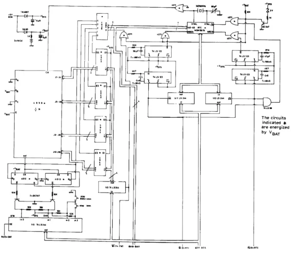
The chosen Sinclair Spectrum microcomputer is not a frame computer and uses non-buffered data, address, and control busses. As additional heavy loads cannot be reliably added on these busses when the Sinclair interface 1 and printer are connected, interfacing the Sinclair Spectrum to other devices starts with buffering of the computer expansion connector signals. Therefore, the first module developed is the interface from the Sinclair Spectrum bus to a buffered and partially decoded local bus (Fig. 2).
The ramp generators can be easily replaced by a time-base module and two digital-to-analog (D/A) converters followed by operational amplifiers to achieve the necessary output swing. This time-base module is, in fact, a real-time clock module housed together with a programmable frequency divider. The real-time clock gives time stamping information while the divider generates the sample command to the computer.
Emulation of the multichannel analyzer requires a display module with reasonable resolution to give permanent information about the scan in progress and keep the computer display dedicated to permanent status information only. The analyzer RS-232 link is replaced by a 16 bit parallel interface to the main TN-4000 computer and is located in the interface module for hardware reasons. Finally, an A/D module converts the ion current for the Sinclair computer.
Control of the quadrupole mass spectrometer and electron multiplier high voltage supply is achieved by two D/A converters and a programmable HV supply. Depending on the mass spectrometer used, the mass control could be more or less easily realized but should never ask for more than a few isolated operational amplifiers. These two later DACs are located together with the ramp generator DACs and status information leds in the same module.
Fig. 2. General architecture of the automated experiment.
Later, a peak meter module was added to monitor the level at the A/D converter input. This peak meter is completely independent of the computer.
Remote programming of the electron beam current, focus electrodes potential, L, and ion acceleration potential, Al, A2, is of little use as their values are seldom modified. These controls may remain manual without any loss in flexibility of the system.
HARDWARE ORGANIZATION
Except for the computer, interface 1, and printer, the system is housed in a NIM rack with NIM power supplies. In our case, the NIM system was used to remain compatible with other previous equipment but the implementation of the system is not packaging-dependent and could be implemented with any other packaging style. Alternative packaging choices can further reduce the total cost of the system, but the construction details, such as printed circuits, can only be given for NIM or other implementations which are compatible in size.
The D/A converter module uses a double width NIM unit while the others use single width units. Available voltages from the backplane connectors are + 6, + 24, +12, -12 and, -24 volts. The D/A converter module and high voltage power supply need the A.C. line voltage which must be introduced separately. Power drain has been reduced to a minimum by the use of CMOS or NMOS technology where it was possible.
The usual + 5 V logic supply voltage is roughly generated from the + 6 V by the use of the forward dropout of a silicon diode followed by a filtering capacitor to reduce the internal impedance of this supply. A low dropout regulator such as LM2940CT5.0 could also be used but seems unnecessary.
decoding circuitry in the same module. For a limited system size, this causes no restriction and reduces overall cost. This local bus consists of a buffered data bus, four buffered address lines, and 16 write/8 read select lines. Adding a ground line to these signals gives a total of 37 lines which is well adapted to common D-type connectors. For short lengths, press-fit male D connectors on a flat cable make a very easily realized back plane which can be readily extended by the addition of a new connector.
A common problem with NIM modules is the lack of room on the rear panel. About one third of it is reserved for the power supply back plane and 7 cm to the local bus D connector. This leaves about 4 cm for the input/output plugs and corresponds to a maximum of 4 BNC plugs on a single-width NIM module. If modules with complex or numerous connectors must be designed, this can be a limitation and large NIM modules or an alternative packaging system should be used.
INTERFACE MODULE
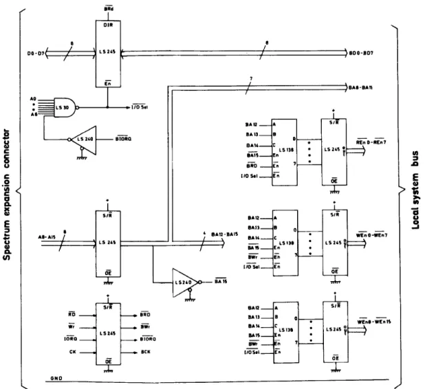
Local bus interface (Fig. 3)
In the ZX Spectrum computer, only partial decoding is applied to the address bus during IN/OUT accesses. This leaves available to the user the address slots for which A0,...,A4 = 1. This corresponds to the 8 slots IF, 3F,..., FF. Fortunately, the indirect addressing input/output Z80 instructions allow the specification of the high byte of the address word.
Fig. 3. Sinclair Spectrum expansion bus to local bus interface.
X stands for any hexadecimal value) and this allows for 256 single-byte input/output devices. One 74LS30 NAND gate and one inverter (1/6 74LS240) decode the local bus address slot and enables the local bus data buffer (74LS245). Partial decoding is performed on the high byte of the address word (A12-A15) to give 16 write (-WEn) and 8 read (-REn) select lines. The remaining A8, A9, A10 and All address signals are buffered and sent to the local bus (BA8... BA11). Each of these select lines give write or read access to 16 inputs or outputs and any further decoding is achieved in the application module when necessary. These select lines are buffered to improve the noise immunity of the local bus. The clock line CK is not used in this application but has been added to the set for completeness.
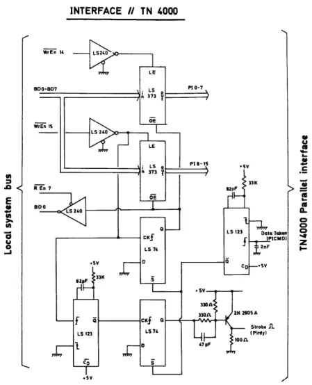
Parallel interface (Fig. 4)
The TN-4000 parallel input port uses a 16-bit-wide bus and two handshake signals. PIRDY indicates to the TN-4000 that valid data has been latched for transfer while PICMD is a TN-4000 answer flag pulsed high when this data has been taken.
To begin a data transfer between the ZX Spectrum and TN-4000 computer, the TN-4000 PICMD flag is first cleared then asserted. This pulses the upper 74LS123 monostable and sets the 74LS74 flip-flops which in turn deactivate the strobe signal PIRDY.
Fig. 4. Local bus to TN-4000 parallel input interface.
The ZX Spectrum verifies that the data in the latches has been taken by reading the status flag from the upper 74LS74 flip-flop located at the I/O address 7XFF and verifying that the lower bit D0 is cleared. When the
status flag is cleared, the low byte of the 16 bit word is written at I/O address EXFF and the high byte at address FXFF in two 74LS373 latches. Writing the high byte clears the status flip-flop and sets the strobe PIRDY high after the insertion of a small delay by a monostable multivibrator. This delay ensures that the Z80 write access to the 74LS373 is complete when the strobe pulse is asserted. The TN-4000 may now take the data word and pulse PICMD. This procedure is repeated until the last word has been transferred.
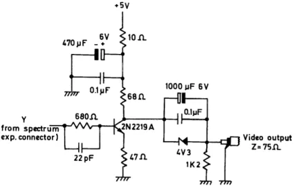
Video interface (Fig. 5)
The video interface consists of a low gain (1.5) inverting amplifier. The luminance Y output of the ULA chip in the ZX Spectrum computer is protected by a series 680 Ω resistor. The d.c. component at the collector of the transistor is removed by a Zener diode, capacitor, and resistor network. The large 1000 µF is necessary to ensure the black level stability during a frame. The 0.1 µF transmits the high-frequency components of the luminance signal. Very often, black level restoration is applied in the video monitor and the zener and resistor can be removed.
When the Y luminance line runs along the other ZX computer bus signals, excessive noise can be induced, but this problem can be easily solved by using white ink on black paper instead of black ink on white paper. If black paper can not be used for a particular application, the Y line should be screened carefully.
Fig. 5. Sinclair Spectrum video interface.
DISPLAY MODULE
The display module is able to show a single curve on a low-cost oscilloscope; the vertical resolution is 12 bits and the total number of channels is 1024. To reduce the Z80 CPU overheads, the module houses its own memory and refresh circuitry. A similar display coupled with its own acquisition system has been described [5].
Display hardware (Fig. 6)
The display interface generates X, Y, and Z signals for a low bandwidth oscilloscope. A 10-bit counter generates select addresses in a 1K × 12 static memory bank. The addresses and memory data are converted into a voltage by two LM1220LCN DACs and two LF353 fast operational amplifiers. The DAC references can be varied to match the X and Y output swing to the scope sensitivity. X and Y multiplication by a factor of 2" is performed by increasing the operational amplifier gain 2" times and clearing the n MSB bits at the DAC inputs. This method gives automatic display wraparound at a very low expense in complexity. Each clock pulse at the input of the address counters triggers a monostable (1/2 CD4538) and generates a short blanking pulse that can be used along with the Z input of the scope to enhance the display clarity. Blanking time, amplitude, polarity, and coupling can be adapted to a wide range of situations.
Fig. 6. Display module.
Computer access to the display is easily implemented. An RS flip-flop made of two 4001 gates stores the display status. If WEn is high, the display is being written; if REn is high (REn = - WEn), display refresh is operating. To write data in the display, the CPU begins by writing a dummy data byte at address BA8 = 1, BA9 = 0. This access sets WEn high, inhibits the clock path from the CD4093 Schmitt-trigger oscillator to the address counters and clears these counters. Data can now be written into channel 0. First, the low byte is written at bus address BA8 = 0, BA9 = 1 and the high nibble is then written at bus address BA8 = BA9 = 1. The end of the second write pulse triggers a monostable (1/2 CD4538) and increments the address counters to point to the next channel. Data writing is repeated until the last channel and a dummy data byte is finally sent to the display at address BA8 = BA9 = 0 to resume write mode and start refresh.
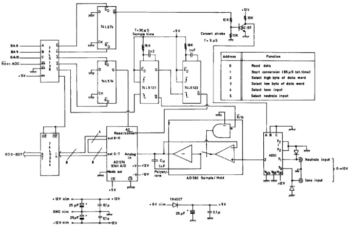
ANALOG-TO-DIGITAL INTERFACE MODULE
The D/A converter module (Fig. 7) is a 12 bit, 2 inputs acquisition module. The input range is 0 to +10 V and total conversion time is 65 µS.Analog input selection is achieved by the use of an analog multiplexer (CD4051, 2 inputs used) protected against negative input voltages by two silicon diodes. Reading dummy data at address BA8 = BA9 = 0, BA10 = 1 selects input 0, while reading at address BA8 = BA10 = 1, BA9 = 0 selects input 1. The multiplexer output is fed into an AD 582 fast sample and hold circuit.
Fig. 7. Analog-to-digital interface module.
Sample function is started by reading at address BA8 = 1, BA10 = BA9 = 0. This triggers the 30 µs sample pulse generated by a 74LS123 monostable. The end of the sample pulse triggers the ADC start convert pulse through the use of a second 74LS123 monostable. After a 65 µs program delay loop allowing for the sample time and the 30 µs AD574 ADC conversion time, the low result byte is selected with a read access at address BA8 = BA10 = 0, BA9 = 1 and the data is read at address BA8 = BA9 = BA10 = 0. This operation is repeated at address BA8 = BA9 = 1, BA10 = 0 and the high data nibble is taken at address BA8 = BA9 = BA10 = 0.
DIGITAL-TO-ANALOG CONVERTER MODULE
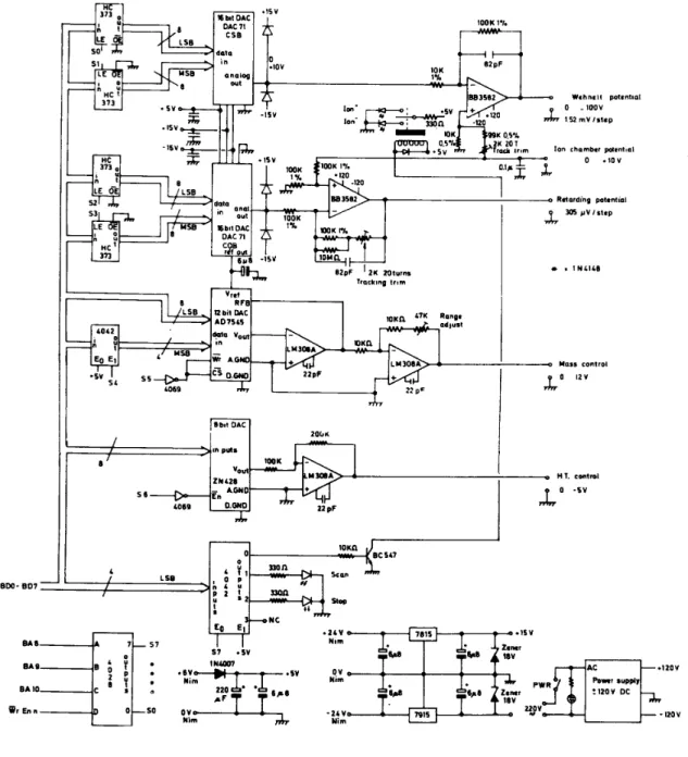
This module controls the electron energy, retarding potential, ion mass selection, and electron multiplier supply voltage (Fig. 8).
The electron multiplier supply is remote controlled by an external voltage in the range 0 to - 5 V for a 0-3000 V output. This remote control voltage is generated by a ZN428 DAC followed by a -2 gain amplifier. The reference and data latch are included in the DAC.
Mass control needs a more precise converter (about 40 steps per mass unit) in order to give accurate mass centering. The AD7545 DAC used is a 12 bit DAC with internal latch. As the 8 LSB bits cannot be written in the DAC separately from the 4 MSB bits, a CD4042 four bit latch has been inserted between the local data bus and DAC MSB bits. The MSB data is written first in this latch and a subsequent writing of the 8 LSB bits transfers all the 12 bit data word in the DAC internal latch. Due to the 0- + 12 V mass spectrometer control voltage range higher than the 7.5 V bandgap reference, the output of the first operational amplifier is further multiplied by a gain factor of about 1.5.
As the electron energy is determined by the Wehnelt-to-ion chamber potential difference, and the retarding potential by the chamber-to-retarding grid voltage difference, the natural way of doing things would be to tie the ion chamber to ground and generate the Wehnelt and retarding grid voltages. In practice, the ion
accelerating lenses A1 and A2 are grounded and the chamber is at about + 5 V from ground (in the case of positive ions). The two 16 bit DACs used are slightly different; the Wehnelt DAC has a 0- + 10 V output swing while the retarding grid DAC has a symetrical -10 to +10 V output swing in order to accelerate or repel the incoming ions. A high-voltage BB3582J operational amplifier adds the ion chamber potential to the 100 V maximum electron accelerating potential. The DAC output to BB3582 output gain is precisely set to -10 by the use of precision resistors (1% or better). The retarding grid potential is the sum of the chamber potential and retarding potential. A second BB3582J amplifier with precise -1 and +1 gains substracts the DAC output from the chamber potential. The DAG output is programmed to the opposite retarding potential. In each case, an exact +1 gain of the Wehnelt and retarding grid voltage relative to the ion chamber voltage is adjusted with a multiturn trimmer
Fig. 8. Digital-to-analog interface module.
.
The status of the experiment is monitored by a few light-emitting diodes and written by the CPU in a four bits latch. The start and stop LEDs indicate if scanning is in progress, stopped, or will stop at the end of the current scan. The ion+/ion- LEDs show the polarity of the analyzed ions. At the present time, only positive ions
have been investigated, but conversion to negative ions is DAC module-independent and this information is displayed for user's convenience only.
REAL-TIME CLOCK MODULE
The real-time clock module provides time information, sampling pulses to the CPU, and is the source of the stop commands issued during scan operation to the computer (Fig. 9). It is based on a MSM58174 RTC chip. This integrated circuit uses a 4 bit data bus and keeps track of time with a precision of 0.1 s. The year information is limited to a leap year/non-leap year flag. Due to the special bus hold time of the RTC, a delay has been inserted in the read (NRDS) and write (NWDS) lines. As the Z80 CPU write timing is different from the read timing, the NWDS monostable pulse is shorter that the NRDS pulse. These timings should be carefully adjusted.
Fig. 9. Real-time clock module.
Power failure is detected by a small Zener/resistor/transistor network. When the power supply drops below 3.5 V, a logic high level is forced by the CD4071 OR gates on the NWDS, NRDS and -CS lines of the RTC and deselects the used outputs of the CD4028 decoder. This inhibits all spurious writing and RTC transient bus contention problems. The RTC clock frequency is derived from a common 32.768 kHz watch crystal adjusted by a small capacitor. The high output impedance and noise sensitivity at the oscillator output requires the use of a CD4071 gate used as an isolation buffer and located as close as possible to the RTC. The clock frequency is divided by a CD4059 programmable divider. The divide modulus is programmed in a BCD format in 4 CD4042 latches and varies from 3 to 9999. The divider output clocks a D flip-flop (1/2 CD4013), indicating that a sampling cycle should be started. This flip-flop should be reset before the next divider pulse or a second D flip-flop (1/2 CD4013) will be set, indicating that a sampling cycle has been missed (over-run error). A 4 bit
buffer transmits to the CPU the data from these two flip-flops and the status of the stop end of scan/stop immediate switches. If the stop EOS switch is depressed, the acquisition will be paused at the end of the current scan. If the stop EOS and stop immediate switches are depressed together, the cycle will be interrupted immediately but it will be impossible to continue the experiment since a scan cycle has been stopped in the middle of the acquisition process.
PROGRAM DESCRIPTION
The control program is divided in two parts. The first part is a Basic program including the menu-driven set-up procedures, display, and transmission utilities. At the top level menu, the user may choose between scan edition, display, transmission, system parameters set-up, and file deletion menus. The most important of these menus is the scan edition menu in which measures can be defined, modified (if possible), examined, and started. At the present time, 10 measures can be programmed at once, but this could be easily increased if enhanced display management procedures were used. The start option transfers all measure parameters in a reserved zone in RAM and calls the machine code acquisition routine. The RTC module switches are scanned after each dwell time period to search for a stop end of scan or stop immediate condition. The program protects the user from further parameter modification when a measure is started. However, a deprotected facility has been added to enable the user to modify the "maximum number of scans" value. When this last scan is complete, the machine code routine gives control back to the Basic program, prints the measure parameters and saves these parameters together with the measure data block on microdrive. The measure is then discarded and the next one (if any) started.
A few other independent machine code procedures are also used by the Basic program. Some of them could be implemented in Basic but, in general, speed reasons dictated the use of a faster language in particular areas of the program. For example, the real-time clock registers must all be read within 0.1 s, which is difficult to achieve with simple peek and poke instructions in Basic. The transmission routine is also written in machine code as this simple modification could drastically improve the transmission speed. The total transmission time is 0.5 s in machine code versus the previous 10 min with the multichannel analyzer. When this routine is written in Basic, a transmission time of 40 s is the minimum that can be reached.
The limitations of this acquisition program are related to the machine code procedures speed and free RAM left to the programmer. For the present implementation, the dwell time can be varied from 25 ms to 0.3 s and dead time between successive scans is programmable from 1 to 59 s. Each measure is stored on the microdrive as a 6 kB binary file and for a mean 85 kB cartridge capacity, 14 files can be saved on it. This being superior to the 10 measures buffer, a complete measuring session can be run on a stand-alone basis. In case of error, the system prints the status of the experiment and waits in the scan edition menu until the operator takes the appropriate correcting action. In normal operation, no errors should occur as the Basic program traps all incoherent parameters that could be introduced by the user.
CONCLUSION
This new set-up increased the productivity of the experiment by at least a factor of three. This has been observed over a non-stop period of 9 months.
During that time, the system was shown to be reliable and no failures have been observed.
The use of a low cost Sinclair Spectrum computer might at first seem to be a limitation when other workers use mostly large, expandable personal computers or even mainframe computers. However, if a more efficient central computer is used for main storage and spectral data manipulations, a small amount of hardware is sufficient to control completely a slow acquisition experiment. This architecture makes the use of high-end multi-tasking or multi-user software and hardware unnecessary while keeping the computing power of the central computer intact. The low complexity of a Sinclair Spectrum computer may even be understood as a facility when it reduces the interfacing hardware complexity and makes the realization of circuits adapted to special requirements easier.
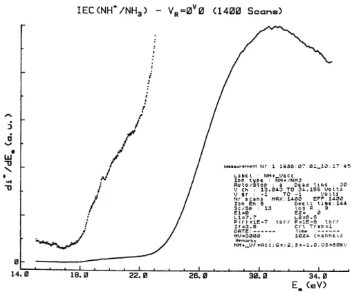
A sample ionization efficiency curve is shown in Fig. 10 with its related, parameters print out. Compared with the previous manual hardware, the time efficiency and protection from user errors has been greatly improved and from the user side, the control program reduces the time spent in fixing the many different scan parameters. The same automation work has been adapted to a photo-ionization experiment with little modification in the hardware and software.
Construction details and control program listings are available upon request from the authors and, in answer to demands from other research groups, a description of the integro-differentiator used will be published in the near future.
Fig. 10. Ionization efficiency curve and parameters print out of NH+/NH3 recorded with the actual automated
system.
ACKNOWLEDGEMENTS
This work has been performed within the framework of the Belgian program for the reinforcement of the scientific potential in new technologies, PREST (Prime Minister's Office for Science Policy). Scientific responsibility is assumed by the authors. One of us (Ch.S.) wishes to thank the Belgian Ministry of Scientific Policy for a PREST grant, and the Université de Liège and the Fonds de la Recherche Fondamentale Collective for financial support.
REFERENCES
1 L.W. Green, J.S. Barsczewsky and N.L. Elliot, Int. J. Mass Spectrom. Ion Processes, 67 (1985) 253.
2 P.L. Fisher and R.L. Cone, Rev. Sci. Instrum., 53 (1982) 634.
3 J.J. Butler, D.M.P. Holland, A.C. Parr, R. Stockbauer and R. Buff, J. Phys. E, 18 (1985) 286.
4 R. Locht and J. Schopman, Int. J. Mass Spectrom. Ion Phys., 15 (1974) 361.
5 T. Cosgrove, J.S. Littler and K. Stewart, J. Phys. E, 13 (1980) 821.