HAL Id: tel-02024207
https://pastel.archives-ouvertes.fr/tel-02024207
Submitted on 19 Feb 2019
HAL is a multi-disciplinary open access
archive for the deposit and dissemination of sci-entific research documents, whether they are pub-lished or not. The documents may come from teaching and research institutions in France or abroad, or from public or private research centers.
L’archive ouverte pluridisciplinaire HAL, est destinée au dépôt et à la diffusion de documents scientifiques de niveau recherche, publiés ou non, émanant des établissements d’enseignement et de recherche français ou étrangers, des laboratoires publics ou privés.
Irradiation effect in triple junction solar cells for spatial
applications
Seonyong Park
To cite this version:
Seonyong Park. Irradiation effect in triple junction solar cells for spatial applications. Atomic Physics [physics.atom-ph]. Université Paris Saclay (COmUE), 2018. English. �NNT : 2018SACLX039�. �tel-02024207�
Influence de l’irradiation dans les
cellules solaires triple jonctions
pour des applications spatiales
Thèse de doctorat de l'Université Paris-Saclay
préparée à É cole Polytechnique
É cole doctorale n°573 Interfaces : approches interdisciplinaires,
fondements, applications et innovations (Interfaces)
Spécialité de doctorat : Physique
Thèse présentée et soutenue à Palaiseau, le 10 juillet 2018, par
M. Seonyong Park
Composition du Jury : M. Yvan Bonnassieux
Professeur, LPICM, É cole Polytechnique Président
Mme. Marie France Barthe
Directrice de recherche, CEMHTI, CNRS Rapporteur
M. Stefan Janz
Chef du département, Fraunhofer ISE Rapporteur
M. Claus Zimmermann
Expert senior, Airbus DS GmbH Examinateur
M. Carsten Baur
Ingénieur, ESA ESTEC Examinateur
M. Erik Johnson
Chargé de recherche, LPICM, É cole Polytechnique Examinateur
M. Bruno Boizot
Responsable accélérateur, LSI, É cole Polytechnique Directeur de thèse
M. Victor Khorenko
Chef de projet R&D, AZUR Space Solar Power GmbH Invité
NNT
:
201
8
SA
CLX03
9
THESE DE DOCTORAT
DE L’UNIVERSITE PARIS-SACLAY
Préparée à
L’ECOLE POLYTECHNIQUE
ECOLE DOCTORALE N°573
Interfaces (EDI)
Spécialité de doctorat : Physique
par
Seonyong Park
Influence de l’irradiation dans les cellules solaires
triple junctions pour les applications spatiales
Cette thèse a été soutenue le 10 juillet 2018 à 14h00
Amphithéâtre Becquerel – Ecole Polytechnique
Composition du jury :
Marie France Barthe
(CNRS CEMHTI Orléans)
Rapporteur
Stefan Janz
(Fraunhofer ISE)
Rapporteur
Yvan Bonnassieux
(Ecole Polytechnique)
Président du jury
Erik Johnson
(Ecole Polytechnique)
Examinateur
Claus Zimmermann
(Airbus Defence and Space)
Examinateur
Carsten Baur
(ESA ESTEC)
Examinateur
Victor Khorenko
(Azurspace Solar Power)
Invité
5
Acknowledgements
I firstly want to thank Dr. Stefan Janz and Dr. Marie France Barthe, who accepted to review this thesis manuscript, as well as Pr. Yvan Bonnassieux, Dr. Erik Johnson, Dr. Claus Zimmermann, Dr. Carsten Baur for accepting to be part of jury and Dr. Victor Khorenko for accepting the invitation.
I am most grateful to my supervisor, Dr. Bruno Boizot, for his excellent guiding throughout these three years and half. You were always so patient even when I was little bit lost and you led me to the good direction. I would also express my greatest gratitude for that you gave me a lot of opportunities such as to participate in several European projects, to attend to big international conferences and so many big and small things. I want to thank Dr. Jacques C. Bourgoin for his insightful guidance on tricky questions related to radiation induced defects in LILT condition. A great part of my thesis could be succeeded thanks to his effort.
I am indebted to Olivier Cavani who is the true master of electron accelerator. Without his work, it was impossible to obtain such nice experimental results. Whenever I had a trouble or difficulty with my equipment, you always brought me generous solutions! Your problem-solving thinking has inspired me tremendously.
I dearly thank Prof. Kyu Chang Park who taught me during the first year of master degree. You permitted for me to freely explorer the experimental physics and again I thank Dr. Erik Johnson for accepting me as an internship student in your team. It was a great chance for me to start the solar cell physics. In addition, I want to thank all professors at Kyung-Hee University and at Ecole Polytechnique who taught me invaluable courses. Your classes contributed a lot to make me a professional person to physics, material science and electrical engineering from my undergraduate to master period.
I am sincerely thankful to all my French speaking colleagues! You trained me a lot (even if you weren’t aware of it). C’est devenu mon grand atout et ma capacité importante.
Throughout my studying in France, I was never lonely because I had many priceless best friends Jinwoo Choi, Heechul Woo, Heejae Lee, Heeryung Lee and all from EP-KHU program. Especially, I can’t imagine how it would be different if Thomas Sanghyuk Yoo was not here. Thank you all for spending your precious time with me. I will never regret spending a huge part of my ‘jeunesse’ at LSI, Ecole Polytechnique Campus and in France. I also thank my friends in Korea, in France and in all of the world, and my parents and sister who have always believed me and cheered me up. Your support has become a great energy for me.
Et fin vraiment, merci beaucoup Virginie, j’exprime ma chaleureuse reconnaissance à toi pour ton soutien et support avec une grande patience et ton grand amour. Si je n’étais pas avec toi, comment pourrais-je supporter ses longues années de doctorat ? Je ne peux même pas l’imaginer. É galement, je saurais gré à ta famille qui m’a inconditionnellement encouragé.
6
Content
Acknowledgements ... 5
General introduction ... 9
1
Fundamentals of solar cells for space applications ... 13
Basics of Photovoltaics ... 14
1.1.1 Basic solar cell equations ... 14
1.1.2 Diffusion current ... 18
1.1.3 Generation-recombination current ... 20
1.1.4 Temperature dependence of solar cells... 22
1.1.5 Spectral response of PN solar cells ... 24
Theoretical aspect of radiation damage ... 27
1.2.1 Displacement damage and atomic displacement ... 28
1.2.2 Primary and secondary displacements ... 30
1.2.3 Ionization ... 33
Nature of irradiation-induced defects in solar cell materials ... 34
1.3.1 Production of defects in n- and p-doped Galium-Arsenide (GaAs) ... 35
1.3.2 Production of defects in n- and p-doped Galium-Indium-Phosphide (GaInP) ... 40
1.3.3 Production of defects in n- and p-doped Germanium (Ge) ... 45
Mechanism of the degradation induced by the defects ... 49
1.4.1 Effects in carrier lifetime and diffusion length ... 49
1.4.2 Effects in properties of solar cells ... 50
Simulation of radiation effects in solar cells ... 51
1.5.1 The concept of equivalent damage (JPL method) ... 51
1.5.2 The concept of displacement damage dose (NRL method) ... 51
Conclusion of the chapter 1 ... 52
Reference ... 54
2
Experimental details and Materials ... 58
Low Intensity Low Temperature (LILT) measurement system setup ... 59
2.1.1 Irradiation Facilities ... 60
2.1.2 Solar Simulator ... 64
7
Structure of lattice matched GaInP/GaAs/Ge triple junction solar cell ... 69
Photon recycling effect in a component cell ... 71
In-situ characterization of TJ cells and its component cells ... 75
2.4.1 Indirect temperature measurement ... 75
2.4.2 Beginning Of Life performance of the cells ... 79
2.4.3 Electron and proton irradiation campaigns ... 83
References ... 89
3
Proton irradiation ... 90
Proton irradiation of TJ cells in LILT conditions ... 92
3.1.1 Analysis of I-V characteristics before and after 1 MeV proton irradiations ... 93
3.1.2 Degradation of key parameters in TJ cells ... 94
Approach to the component cells ... 95
3.2.1 Degradation of ISC and VOC at different temperatures ... 95
3.2.2 Electric field dependence of I-V characteristics ... 100
3.2.3 Orientation dependence of proton irradiation ... 102
3.2.4 Isochronal annealing in component cells ... 108
Discussion of the chapter 3 ... 110
3.3.1 Temperature and fluence dependences of the degradation ... 110
3.3.2 Recovery of proton irradiation-induced defects ... 113
3.3.3 Recombination of photo generated current by irradiation-induced defects ... 114
Conclusion of the chapter 3 ... 116
Reference ... 117
4
Electron irradiation ... 119
Irradiation of TJ cells in LILT conditions ... 120
4.1.1 Analysis of I-V characteristics before and after 1 MeV electron irradiations ... 121
4.1.2 Degradation of key parameters in TJ cells ... 125
Approach to the component cells ... 126
4.2.1 Degradation of ISC and VOC at different temperatures ... 126
4.2.2 The excess leakage current in dark I-V characteristics... 128
Annealing effect of electron irradiated cells ... 133
Discussion of the chapter 4 ... 134
4.4.1 Uncertainty of the TJ cell degradation induced by electron irradiations ... 134
4.4.2 Origin of the excess current ... 135
8
Reference ... 138
5
General discussion ... 140
Comparison of electron and proton irradiation in LILT conditions ... 141
Distribution of BOL and EOL data set: Case of electron and proton irradiated TJ
cells
149
Correlation of radiation induced defects with electrical property of the solar cell
151
Conclusion of the chapter 5 ... 153
Reference ... 154
General Conclusions ... 155
Annexe – Résumé de thèse en français ... 157
List of Publications ... 162
List of Figures ... 163
9
General introduction
The history of solar cell has begun since 1839 by a great discovery of a French physicist Edmond Becquerel about the production of an electrical charge in solution by the light source. Then, during the late 19th century, there were some scientific researches related to the photovoltaic (PV) effect. For example, a discovery of PV effect in solids at 1870 and a discovery of a Selenium PV with ~1 % efficiency at 1880. However, these scientific works did not gain a big interest from the energy industry. At 1905, Albert Einstein published an article about the photoelectric effect based on the quantum bias. Much later, at 1950, there was a great improvement on single crystal solar cell using a crystallization technique called as Czochralski (CZ) Method developed by a Polish chemist Jan Czochralski. Since then, the solar cell technology has been highlighted as a new source to generate electricity. The photo conversion efficiency was hugely increased up to more than 10 % thanks to the CZ crystallization method. Few years later, the first practical solar cell based on a single crystal silicon was invented by Bell Labs at 1950s. This solar cell was designed to be equipped to a satellite, having an average efficiency of 10 %.
Figure 0-1. the first solar powered satellite Vanguard 11.
The satellite named Vanguard 1 was the first solar cell powered satellite (and 4th artificial Earth satellite). The Vanguard 1 was launched at 1958 and is still orbiting the Earth! This event is generally considered as a birth of commercial space application of PV. After few decades, at 1970s, the energy crisis occurred and this triggered the research on PV. As shown in Figure 0-2, since late 1970s, many researchers have been dedicated to the development of PV technologies. Today, in many different ways (based on silicon, germanium, III-V compounds such as GaAs, CIGS, CdTe, dye sensitized cells, perovskite cells, …), researches are ongoing to extend the knowledge on PV and to apply it as a renewable energy source.
10
Early age of space industry, on the most of solar powered satellites, single crystalline silicon based solar panels were equipped. However, the silicon based solar cell inherently exhibited worse characteristics under the low temperature, the weak light intensity and radiation exposure condition than gallium arsenide (GaAs) based solar cells. One of main reasons of not using the GaAs crystal is because of the expensive cost for the fabrication such as MBE and MOCVD processes.
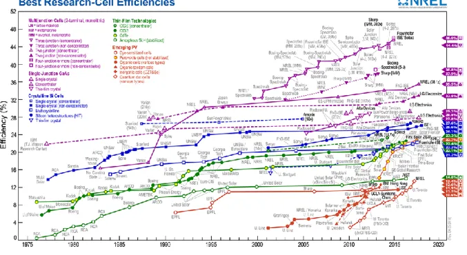
Figure 0-2. Chart of best research-cell efficiencies updated by NREL at 25/04/20182.
Once these technologies become matured, the GaAs based solar cells have been used widely for solar powered satellites (SPS) and concentrated photovoltaics (CPVs). For both SPS and CPVs, the highest achievable efficiency was the main interest. Consequently, multijunction cells were developed at the beginning of 2000s, and today, the state of the art multijunction cell is so called triple junction solar cells based on gallium-arsenide (GaAs), gallium-indium-phosphor (GaInP) and germanium (Ge). More recently, NASA launched a space probe named Juno at 2011 for the explorer mission of the Jupiter.
11
Figure 0-3. Juno mission to Jupiter (2010 Artist’s concept)3.
The GaInP/GaAs/Ge based triple junction solar cell was first used for the deep space explorer mission. In succession to Juno, ESA will launch their spacecraft at 2022. The mission named JUICE4 is the first large class mission in ESA’s cosmic vision 2015-2025 program to explore the gigantic gaseous planet Jupiter and its moons, Ganymede, Callisto and Europa. The Jupiter’s environment which is called as Jovian system is surrounded by a huge magnetic field of the Jupiter. Particles such as electrons and protons which are come out from the Sun are captured by the magnetic field, and then get accelerated by Lorentz force. Up to here, the situation sounds similar to the orbit of the earth. However, it must be also considered that Jupiter is very far from the Sun and that the intensity of the solar spectrum is going down to only 3.7 % of AM0. Furthermore, the absolute temperature in average is about 120 K near Jupiter, while the average temperature near the Earth is supposed to be 300 K. In order to successfully perform the ESA missions, evaluating an accurate end of life performance of the solar cell which will be equipped to the spacecraft is one of the prime importance. In this frame, LSI has participated to the JUICE annealing verification study, performing the electron irradiation with their SIRIUS electron accelerator and the proton irradiation at CSNSM in University of Paris-Sud in Orsay.
3https://www.jpl.nasa.gov/news/news.php?feature=4818 4Jupiter Icy Moon Explorer
12
Figure 0-4. Artist's impression of JUICE mission5.
Performing the irradiation test on the state of the art GaInP/GaAs/Ge triple junction (TJ) solar cell for JUICE mission, scientific questions concerning their behavior in deep space condition like near Jupiter have arisen. Thus, through this thesis work, we will try to find answers to some questions like defects generation in complex TJ solar cells as a function irradiation temperature, fluences and the nature of the particle and the influence of these defects on the TJ cells electrical properties. For that purpose, the
Chapter 1 will present some fundamental knowledge to understand the physics of solar cell, theory of
radiation damage, nature of radiation induced defects in semiconductors, and the simulation of solar cell degradation by radiation exposure in space. In chapter 2, we will be introducing irradiation facilities and experimental instruments for measurements. Then, non-irradiated samples will be described. Lastly, the irradiation steps and data treatment will be discussed. Subsequently, we will be separately focusing on the aspect of electron and proton irradiations of TJ solar cells in Low Intensity Low Temperature (LILT) conditions in chapter 3 and chapter 4, respectively. In chapter 5, we will generally discuss the effect of electron and proton irradiations, correlating the degradation with nature of radiation induced defects. At the end of this book, we will briefly conclude our research and let some perspectives to be continued in near future.
13
1 Fundamentals of solar cells for space
applications
1.1
Basics of Photovoltaics ... 14
1.1.1 Basic solar cell equations ... 14
1.1.2 Diffusion current ... 18
1.1.3 Generation-recombination current ... 20
1.1.4 Temperature dependence of solar cells... 22
1.1.5 Spectral response of PN solar cells ... 24
1.2
Theoretical aspect of radiation damage ... 27
1.2.1 Displacement damage and atomic displacement ... 28
1.2.2 Primary and secondary displacements ... 30
1.2.3 Ionization ... 33
1.3
Nature of irradiation-induced defects in solar cell materials ... 34
1.3.1 Production of defects in n- and p-doped Galium-Arsenide(GaAs) ... 35
1.3.2 Production of defects in n- and p-doped Galium-Indium-Phosphide(GaInP) ... 40
1.3.3 Production of defects in n- and p-doped Germanium (Ge) ... 45
1.4
Mechanism of the degradation induced by the defects ... 49
1.4.1 Effects in carrier lifetime and diffusion length ... 49
1.4.2 Effects in properties of solar cells ... 50
1.5
Simulation of radiation effects in solar cells ... 51
1.5.1 The concept of equivalent damage (JPL method) ... 51
1.5.2 The concept of displacement damage dose (NRL method) ... 51
Conclusion of the chapter 1 ... 52
14
The aim of this chapter is to understand the working principle of solar cell and impact of defects induced by radiation on its physical and electrical properties. Therefore, in the physics of photovoltaics, we will first discuss the electrical description of photovoltaic device using the knowledge in semiconductors, then the physics of radiation damage in semiconductor and defect creation in some key solar cell materials will be described. Finally, combining all these aspects, we will describe simulation techniques which are currently well adapted to the space solar cell research and industry.
1.1 Basics of Photovoltaics
Photovoltaics means by the definition that the conversion of light energy into the electricity occurring in semiconducting materials. It is also referred as photovoltaic effects, and when this type of semiconducting materials is used for the purpose of harvesting light energy, it is called solar cell (or solar panel for large area with interconnection). These days, photovoltaic effects are being studied in several domains not only in physics, but also photochemistry and electrochemistry. In addition, there exists numerous different solar cells architecture from inorganic solar cells based on Silicon (Si) or III-V compounds to recently highlighted Perovskite solar cells [1]. Inorganic solar cells are now well commercialized while other solar cell technologies are still in development by a lot of researchers in the world. In principle, solar panels are installed where sustainable energy production is required. For terrestrial use, a solar settlement system on roofs can be considered for examples for cities and solar farms (also known as a photovoltaics power station) in case of large scale areas such as deserts and agricultural areas. For spatial use, solar panels are equipped to the body of satellites and spacecrafts or installed as wings which can be rotated to maximize the absorption of solar spectrum in any conditions. Since the space solar cells are exposed in very extreme conditions (huge variation of temperature, radiation and intensity of solar spectrum), solar cell engineers have developed space relevant experiment systems in laboratories to simulate solar cells in space conditions and simulation techniques to predict their performances in different space conditions. This will be discussed at the end of this chapter. In this sub-chapter, we will first discuss the physical understanding of solar cell operation.
1.1.1 Basic solar cell equations
Figure 1-1 shows an equivalent circuit diagram of an illuminated solar cell. It describes a combination of current generation by light absorption in semiconducting materials and loss mechanism due to several causes. The light absorption is represented by the light generator symbol. As shown in this diagram, there are two diodes in parallel together with the light generator. The first diode (D1) illustrates a
bias-dependent dark current (I1), which is considered to originate from the diffusion of minority carriers into
its neighboring n- or p- type layer. The second diode (D2) indicates a current flow by the carrier
generation and recombination via defects which are located in depletion region (I2). Finally, the third
15
Thus, these three currents flow to reverse direction from the direction of the light generation current (Iph).
Figure 1-1. Equivalent circuit diagram of an illuminated solar cell based on two diodes model.
Eq. (1-1) represents the diode equation of a solar cell, under illumination, that has two diodes by the reason explained above. The current which arrives to an external circuit is the result of subtraction of I1,
I2 and Ish from Iph. Each term of I1 and I2 is described with Shockley diode equation and saturation current
(I01 and I02) typically defined by the material’s semiconducting property and temperature.
𝐼 = 𝐼𝑝ℎ− 𝐼01[𝑒𝑥𝑝 (𝑞(𝑉 + 𝐼𝑅𝑠) 𝑘𝑇 ) − 1] − 𝐼02[𝑒𝑥𝑝 ( 𝑞(𝑉 + 𝐼𝑅𝑠) 2𝑘𝑇 ) − 1] − 𝑉 + 𝐼𝑅𝑠 𝑅𝑠ℎ (1-1)
In the diode equation, q is a charge of electron, k is Boltzmann constant, Rs is series resistance, and T is
kelvin temperature (K). It can be also written as Eq. (1-2) to simplify the equation.
𝐼 = 𝐼𝑝ℎ− 𝐼1− 𝐼2− 𝐼𝑠ℎ (1-2)
In order to simplify the diode equation of a solar cell, two diodes terms in the equation can be replaced by one diode term which have an ideality factor n. the ideality factor ranges between 1 and 2 depending on whether the diffusion current or the generation-recombination current is dominant and it can be varied along with operating voltage. Furthermore, saturation currents by diffusion and recombination-generation are unified into one parameter I0.
𝐼 = 𝐼𝑝ℎ− 𝐼0[𝑒𝑥𝑝 (𝑞(𝑉 + 𝐼𝑅𝑠)
𝑛𝑘𝑇 ) − 1] −
𝑉 + 𝐼𝑅𝑠
𝑅𝑠ℎ (1-3)
In most solar cells, the series resistance is small (Rs < 0.1 ohms) and the shunt resistance is large (Rsh >
1x10⁴ ohms). Terms involving Rs and/or Rsh in Eq. (1-3) is relatively too small to affect to I-V
characteristics compared to other terms. Thus, neglecting these small terms, the equation is again simplified as below:
16
𝐼 = 𝐼𝑝ℎ− 𝐼0[𝑒𝑥𝑝 (𝑞𝑉
𝑛𝑘𝑇) − 1] (1-4)
This basic solar cell equation is mostly used in practice. For a single junction solar cell, assuming that minority carrier lifetime of two charge neutral regions is sufficiently long, when the cell is illuminated, its current-voltage curve is shifted to -y axis by the amount of photo generated current (Iph). When the
voltage is zero biased, the current that the solar cell exhibits is called as short circuit current (ISC). The
point of voltage where no current flows in the circuit is called open circuit voltage (VOC). The power
consumption of the diode under illumination at fourth quadrant is negative, that is, the cell is delivering power to load. We can also find a maximum power point (PMAX) from the I-V curve. The current and
the voltage where the power is maximum is called IMPP and VMPP, respectively. A representative diagram
is described in Figure 1-2.
Figure 1-2. Current-Voltage (I-V) curve of a solar cell in dark and under illumination.
In fact, from Eq. (1-4), if we know all parameters such as ideality factor n, photo-generated current Iph,
saturation current I0, VOC can be solved (where the current equals to zero):
𝑉𝑂𝐶=𝑛𝑘𝑇 𝑞 𝑙𝑛 ( 𝐼𝑝ℎ 𝐼0 + 1) ≅ 𝑛𝑘𝑇 𝑞 𝑙𝑛 ( 𝐼𝑝ℎ 𝐼0) (1-5)
Theoretical approach to these parameters will be also discussed in this sub-chapter. To evaluate I-V curve of an illuminated solar cell, we also use a parameter called fill factor (FF) which describes a ratio of PMAX versus product ISC and VOC as shown in Eq. (1-6). Through this parameter, one can easily guess
whether the cell is close to the ideal solar cell or it contains anomalies due to series and shunt resistances or other effects related to recombination or tunneling of carriers.
17
𝐹𝐹 = 𝑃𝑀𝐴𝑋 𝐼𝑆𝐶× 𝑉𝑂𝐶 =𝐼𝑀𝑃𝑃× 𝑉𝑀𝑃𝑃 𝐼𝑆𝐶× 𝑉𝑂𝐶 (1-6)If a solar cell behaves like an ideal diode, its FF becomes close to 1 (ISC ≈ IMPP, VOC ≈ VMPP). However,
in reality, this is not possible since the solar cell must have a contact to extract currents from itself (Rs
arises) and the semiconducting material can never be 100 % pure without any defect, especially when doped. This is one of the causes of Rsh. As a consequence, the I-V curve of an illuminated solar cell
behaves like the red curve of Figure 1-3. Conventionally, the I-V curve of illuminated solar cells is inverted as presented below to describe its parameters in positive sign. The effect of shunt resistance is reflected to the slope of linear region close to ISC. As the Rsh becomes smaller from infinity, the flatness
of diode near ISC before its turn-on point decreases (in other word, one can say the slope near ISC increase
in negative direction). On the other hand, when the Rs is larger, the steepness of the slope near VOC
decreases.
Figure 1-3. Conventional I-V curve of an illuminated solar cell (effect of series and shunt resistances on electrical characteristics).
One of the most important parameter in solar cell is photo conversion efficiency (η) which is obtained by dividing the output power (POUT) into the input power (PIN). In general, the maximum efficiency
(𝜂𝑀𝐴𝑋) of the cell is referred as the efficiency of the cell, and for 𝜂𝑀𝐴𝑋, PMAX value is taken.
𝜂 =𝑃𝑂𝑈𝑇
𝑃𝐼𝑁 𝑎𝑛𝑑 𝜂𝑀𝐴𝑋= 𝑃𝑀𝐴𝑋
18
For a solar cell which is based on the single pn junction structure, there is a theoretical limit on its photo conversion efficiency, i.e. Shockley-Queisser limit [2]. To calculate this theoretical limit, Shockley and Queisser have defined the following assumptions:
One photon creates only one electron-hole pair. Cell is illuminated with unconcentrated light.
Thermal relaxation of the electron-hole pair occurs only in excess of the bandgap.
Under these assumptions, the limit of conversion from photo energy to electricity is induced by several physical phenomena such as: blackbody radiation which exists in any material above 0 Kelvin, recombination of electron-hole pairs, spectrum losses (higher energy of photons than the bandgap of material). With a single pn junction solar cell, their calculations predicted the maximum efficiency of around 33.7 % when the cell has a bandgap of 1.4 eV under AM1.5 solar spectrum (1000 W/m2). By
minimizing the losses listed above, developing optimal structure, and purifying materials, some improvement has been made. With single crystalline silicon cells, the efficiency of 26.7 ± 0.5 % has been experimentally realized and with single GaAs junction cells, 28.8 ± 0.9 % has been achieved under the global AM1.5 spectrum (1000 W/m2) at 25 ˚C [1].
On the other hand, there exists many of other researches trying to exceed the limit with different approaches. The most widely taken method to achieve higher efficiency is to fabricate multi junction solar cells (also called as tandem solar cells).
1.1.2 Diffusion current
The diffusion current is composed of majority carrier electrons in n-type material surmounting the electric potential barrier to diffuse to p-type material side and majority carrier holes in p-type material diffusing to n-type side so that they become minority carriers in neighboring p- and n-type side. The hole diffusion current density at any point 𝑥𝑛 in n-type material can be calculated following the equation below: 𝐽𝑝(𝑥𝑛) = −𝑞𝐷𝑝𝑑𝛿𝑝(𝑥𝑛) 𝑑𝑥𝑛 = 𝑞 𝐷𝑝 𝐿𝑝Δ𝑝𝑛𝑒 −𝑥𝑛⁄𝐿𝑝= 𝑞𝐷𝑝 𝐿𝑝𝛿𝑝(𝑥𝑛) (1-8)
where 𝐷𝑝 and 𝐿𝑝 are the diffusion coefficient and the diffusion length of hole, respectively. Then, the
total hole current density near at 𝑥𝑛0 is simply obtained by evaluating Eq. (1-8) at 𝑥𝑛= 0:
𝐽𝑝(𝑥𝑛0) =𝑞𝐷𝑝 𝐿𝑝 Δ𝑝𝑛 = 𝑞𝐷𝑝 𝐿𝑝 𝑝𝑛[𝑒𝑥𝑝 ( 𝑞𝑉 𝑘𝑇) − 1] (1-9)
Similar approach can be applied to the minority carrier electrons in p-type material, then, total current density by diffusion of electrons and holes can be described as:
19
𝐽1= (𝑞𝐷𝑝𝑝𝑛0 𝐿𝑝 + 𝑞𝐷𝑛𝑛𝑝0 𝐿𝑛 ) [𝑒𝑥𝑝 ( 𝑞𝑉 𝑘𝑇) − 1] = 𝐽01[𝑒𝑥𝑝 ( 𝑞𝑉 𝑘𝑇) − 1] (1-10)Eq. (1-10) is the diode equation which we have already seen in Eq. (1-1) for the second term. However, in this case, resistances are not considered. By using a relationship 𝐿𝑝= √𝐷𝑝𝜏𝑝 and 𝐿𝑛= √𝐷𝑛𝜏𝑛,
where 𝜏𝑛 and 𝜏𝑛 are the minority carrier lifetime of holes and electrons, and according to the mass action law, 𝑛𝑝 = 𝑛𝑖2, 𝑛𝑝0 = 𝑛𝑖2⁄𝑝𝑝0 ≈ 𝑛𝑖2⁄𝑁𝐴 most authors are assuming that the concentration of holes in p-type material is approximately the same as the concentration of acceptors, 𝑁𝐴. Similarly, if we consider n-type material, 𝑝𝑛0= 𝑛𝑖2⁄𝑛𝑛0≈ 𝑛𝑖2⁄𝑁𝐷 where 𝑁𝐷 is the concentration of donor. 𝑛𝑖 is intrinsic carrier concentration in semiconductor. Then, Eq. (1-10) may be rewritten as given:
𝐽01= 𝑞𝑛𝑖2[ 1 𝑁𝐷( 𝐷𝑝 𝜏𝑝) 1 2 + 1 𝑁𝐴( 𝐷𝑛 𝜏𝑛) 1 2 ] (1-11)
In fact, for most pn junction solar cells, the doping concentration of n-type and p-type materials is not equivalent. Generally, where 𝑝𝑛0 is much larger than 𝑛𝑝0 (abrupt 𝑝+𝑛 junction), the second term of Eq.
(1-11) is much smaller than the first term. In other word, the diffusion current in n-type region can be neglected as seen in below:
𝐽01= 𝑞𝐷𝑝𝑝𝑛0 𝐿𝑝 = √ 𝐷𝑝 𝜏𝑝 𝑛𝑖2 𝑁𝐷 (1-12)
Eq. (1-12) indicates that we can calculate the reverse-saturation current density by diffusion 𝐽01 once the doping concentration, diffusion coefficient, and carrier lifetime are known.
20
Figure 1-4. A pn junction in forward bias: (a) minority carrier distribution in two side of depletion region with a graphical instruction of distance xn and xp from the interface of depletion and charge neutral regions; (b) band banding diagram with
variation of quasi-Fermi level with position[3].
1.1.3 Generation-recombination current
The term 𝐼2 described in Eq. (1-2) is a current flow by the generation-recombination of carriers in the depletion region. When the thermal equilibrium of a physical system in the junction is broken due to an external cause such as applying voltage, the system tends to turn back to its initial equilibrium state and this phenomenon occurs as generation-recombination current which leads the process. A theory describing this recombination-generation current was first developed by Sah, Noyce, and Shockley in 1957 [4]. To establish their theory, they have made simplified assumptions that lifetimes, mobilities, and doping concentrations on both n- and p-type materials were equals, and that the recombination of carriers were caused only due to a single recombination center in a forbidden level at Et, near intrinsic
Fermi level. Following these assumptions, the generation-recombination rate, U can be described as:
𝑈 = 𝑝𝑛 − 𝑛𝑖
2
21
where 𝜏𝑝0 and 𝜏𝑛0 are the hole and electron lifetimes in heavily doped n- and p-type materials and 𝑛1 and 𝑝1 are the free-carrier densities when the Fermi level is coincided with the trap level:
𝑛1= 𝑁𝐶𝑒𝑥𝑝 (𝐸𝑡− 𝐸𝐶
𝑘𝑇 )
𝑝1 = 𝑁𝑉𝑒𝑥𝑝 (𝐸𝑉− 𝐸𝑡
𝑘𝑇 )
(1-14)
The recombination current density in the depletion region can be obtained by integrating the generation-recombination rate U over the depletion width x:
𝐽𝑟𝑔 = 𝑞 ∫ 𝑈
𝑥2
𝑥1
𝑑𝑥 (1-15)
In forward bias condition, majority carrier electrons in n-type material are injected to the depletion region due to the diffusion process, similar to the holes in p-type materials, and they recombine if significant number of carriers exists in the center of depletion region. Recombination current is dominant in forward bias, and the generation current in depletion region is negligible. The recombination current density is maximum at the center of the depletion width and can be described as:
Ideal Case: 𝐽𝑟 = 𝑞𝑛𝑖𝑊 𝜏0 ∙ 𝑒𝑥𝑝 ( 𝑉 2𝑘𝑇) (𝑉𝑏𝑖− 𝑉) 𝑘𝑇 ∙𝜋 2 (1-16)
where 𝜏0 is the lifetime of electron and hole in the depletion region (assumed that the electron and hole have same lifetime in this calculation).
Under reverse bias, the injection of carriers from charge neutral region to the depletion region abruptly decreases, and the generation current density becomes dominant:
Ideal Case: 𝐽𝑔 =𝑞𝑛𝑖𝑊
2𝜏0 (1-17)
In the more general case of the Sah-Noyce-Shockley (S-N-S) theory, the lifetime of electron and hole carriers are not the same in the depletion region. Thus, Hovel has extended the S-N-S theory [5] and concluded for forward bias,
22
Recombination Current (S-N-S): 𝐽𝑟 = 𝑞𝑛𝑖𝑊 √𝜏𝑝0𝜏𝑛0 ∙ 2 sinh ( 𝑉 2𝑘𝑇) (𝑉𝑏𝑖− 𝑉) 𝑘𝑇 ∙𝜋 2 (1-18)when the applied voltage is higher than 4 kT, but does not exceed Vbi - 10 kT, and the average lifetime
of carriers are computed from lifetimes of electrons and holes at each type of materials. As to the reverse bias condition, the current is dominated by generation,
Generation Current (S-N-S): 𝐽𝑔= 𝑞𝑛𝑖𝑊 2√𝜏𝑝0𝜏𝑛0 [cosh (𝐸𝑡− 𝐸𝑖 𝑘𝑇 + 1 2𝑙𝑛 𝜏𝑝0 𝜏𝑛0)] −1 (1-19)
An extended study has been done with different doping concentrations of each side by Choo [6]. The works of Hovel and Choo has provided more realistic generation - recombination current equation to be applied for a practical diode equation since this extended equation is sufficiently accurate within the limitations of the theory. Note also that, depending on the bias (either forward or reverse), one must use Eq. (1-18) or (1-19) to describe 𝐼2 in Eq. (1-1).
As a matter of historical interest, the generation-recombination current density 𝐽𝑟𝑔 is often denoted by 𝐽02, and can be described as:
𝐽𝑟𝑔 = 𝐽02=𝑞𝑊
2 σ𝑣𝑡ℎ𝑁𝑡𝑛𝑖 (1-20)
Assuming that there exists a single trap in the middle of the bandgap with a density Nt. The lifetime of
carriers in the depletion region, τ, is related to the trap density through:
𝜏𝑝= 1
𝜎𝑝𝑣𝑡ℎ𝑁𝑡 𝑎𝑛𝑑 𝜏𝑛= 1
𝜎𝑛𝑣𝑡ℎ𝑁𝑡 (1-21)
where 𝜎𝑛 and 𝜎𝑝 are the electron and hole capture cross sections, W is the width of the depletion region, and 𝑣𝑡ℎ is the thermal carrier velocity. Through this equation, we can find that the generation-recombination current has a linear dependence on the trap density Nt. Note that, depending on the bias
(forward or reverse), As we will discuss later, we would expect to see the increase of I2 when the solar
cell is exposed to an irradiation.
1.1.4 Temperature dependence of solar cells
Either for terrestrial or for spatial purposes, solar cells are exposed to different temperatures. In semiconducting materials, temperature can affect to the mobility and density of carriers and even the bandgap of the material. Therefore, understanding the effects of changing temperature on the solar cell
23
properties is important. By carefully looking at the diode equation of a solar cell under illumination, we can suspect whether each of component can be affected by the change of temperature. First, the reverse saturation current by diffusion which has been derived in Eq. (1-12) can be rewritten as:
𝐽01= [𝑇3exp (−𝐸𝑔 𝑘𝑇 )] 𝑇
𝛾
2= 𝑇(3+𝛾2)exp (−𝐸𝑔
𝑘𝑇) (1-22)
following the assumption that has been made by Sze [7] (𝐷𝑝⁄ is proportional to 𝑇𝜏𝑝 𝛾 where γ is a
constant). This equation indicates that the terms including temperatures are both proportional to the temperature, therefore, at higher temperature, 𝐽01 becomes larger than at lower temperature. Furthermore, at room temperature, intrinsic carrier concentration for GaAs is about 2x106 cm-3 in comparison to the value for Si of around 1.5x1010 cm-3. This difference results primarily from the difference in bandgap energies. The bandgap energy itself is a function of temperature and is described by Thurmond [8]:
𝐸𝑔(𝑇) = 𝐸𝑔(0) −
𝛼𝑇2
𝑇 + 𝛽 (1-23)
The values of 𝐸𝑔(0), α, and β are given for each material depending on its crystallinity. The crystallinity indicates how perfectly the semiconductor material has a periodic lattice structure. For example in the single crystalline GaAs structure, intrinsic GaAs has 𝐸𝑔 of 1.42 eV at 300 K. But, in high doping condition, its bandgap is narrowed by ∆𝐸𝑔 ≈ 2 ∙ 10−11∙ 𝑁
𝑎−1 2 ⁄
(eV) where 𝑁𝑎 is the concentration of dopant in cm-3 since dopants play as impurities which break the periodicity of GaAs structure. Therefore, the intrinsic carrier concentration of material can also affect 𝐽01 and it is also temperature dependent. In summary, 𝐽01 is obviously temperature dependent, and since this parameter is directly used for calculation of 𝑉𝑂𝐶 (Eq. (1-5)), it is considered to be a factor which decrease 𝑉𝑂𝐶 when temperature increases.
Concerning the generation-recombination current 𝐼2, whether it is forward or reverse biased, it is proportional to 𝑛𝑖, whereas the diffusion current 𝐼1 is proportional to 𝑛𝑖2. As a result, the temperature dependence of 𝐼2 is weaker in exponential term 𝑒𝑥𝑝(−𝐸𝑔⁄2𝑘𝑇), than 𝐼1 in 𝑒𝑥𝑝(−𝐸𝑔⁄𝑘𝑇).
The short circuit current (ISC) under illumination corresponds to the collected electron hole pairs from
photo excitation at zero bias condition. Thus, generation rate over the depth of material, and lifetimes of electron and hole at each side including the depletion region is involved to calculate ISC. It is quite
complex but actual measurement gives a small variation of ISC as a function of temperature. When the
diffusion length of carriers is sufficiently long, ISC can be approximated given by [9]:
24
Where 𝑔0 is generation rate of electron-hole pairs per volume unit. Using the relation of diffusion length, coefficient and lifetime (𝐿 = √𝐷𝜏 ) and Einstein relation ( 𝐷 𝜇⁄ = 𝑘𝑇 𝑞⁄ ), it is possible to find a temperature dependence of diffusion length. Shockley, Read, and Hall [10], [11] have found that the temperature dependence of minority carrier lifetime of electron in p-side and hole in n-side.
𝜏𝑝= 𝜏𝑝0[1 + 𝑒𝑥𝑝 (𝐸𝑇 − 𝐸𝐹
𝑘𝑇 )]
𝜏𝑛= 𝜏𝑛0+ 𝜏𝑝0𝑒𝑥𝑝 (𝐸𝑇+ 𝐸𝐹− 2𝐸𝑖
𝑘𝑇 )
(1-25)
Where 𝜏𝑝0 is the lifetime of hole in n-type material in which all traps are filled, ET is energy level of the
trap, and EF is the Fermi energy level. Similarly, electron lifetime 𝜏𝑛0 can be calculated, where Ei is
intrinsic energy level. Even though Eq. (1-25) contains a temperature term in equation, since the Fermi level is also moved close to the intrinsic energy level, the exponential term remains to be very small. Thus, in both type of materials, lifetime of minority carriers is expected to be a relatively constant in temperature ranges for practical applications. In addition, the diffusion length L is primarily determined by the temperature dependence of the carrier mobility.
In practice, the dependence of ISC on temperature mostly comes from the change of the bandgap. When
temperature increases, the bandgap becomes smaller. Then, more photons with lower energy can have opportunity to excite electrons from the valence to the conduction band creating electron-hole pairs, harvesting more solar energy spectrum, it can eventually cause an increase of ISC.
1.1.5 Spectral response of PN solar cells
The absorption of solar energy is a fundamental of the solar cell operation. It can be also described as the absorption of electromagnetic radiation (or the optical injection of carriers). When incident photons are penetrating a material at a depth 𝑥, the photons can be absorbed with a specific optical absorption rate α(𝜆) depending on its wavelength and the remaining of unabsorbed photons in depth 𝑥 follows the Beer - Lambert law:
𝐹 = 𝐹0𝑒𝑥𝑝[−𝛼(𝜆)𝑥] (1-26)
where 𝐹0 is the total number of incident photons per cm2 per second per unit wavelength. Assuming that all absorbed photons are generating one carrier of each, the generation rate at certain wavelength 𝐺(𝜆) at depth 𝑥 can be determined as:
𝐺(𝜆) = 𝛼(𝜆)𝐹0[1 − 𝑅(𝜆)]𝑒𝑥𝑝[−𝛼(𝜆)𝑥] (1-27)
25
Prior to get into a detail of calculation of photo-generated current, the spectral response of a pn junction solar cell can be simply summarized as:
𝑆𝑅(𝜆) = ∑ 𝐽
𝑞𝐹0(𝜆) (𝐴/𝑊) (1-28)
i.e. total excess current density divided into intensity of total number of incident photons per unit wavelength. Ideally, SR can be 1 if all incident protons produce one excess carrier in a pn junction. In most of cases, the solar cell is operating in low injection condition (concentration of photo generated excess carriers 𝑛𝑝 ≪ 𝑛𝑝0 in p-type material). When excess electron carriers are generated in p-side, a diffusion current occurs aside from the diffusion current in dark under forward bias. Similar to the diffusion current density of diode in dark given by Eq. (1-8), the equation of diffusion hole current density 𝐽𝑛 due to the excess current can be also described by the same mechanism and assuming that
there is no electric field in the charge neutral region, 𝐽𝑛 is given by:
𝐽𝑛= 𝑞𝐷𝑛
𝑑(𝑛𝑝− 𝑛𝑝0)
𝑑𝑥 𝑖𝑛 𝑝 − 𝑡𝑦𝑝𝑒 𝑐𝑒𝑙𝑙𝑠 (1-29)
And similarly, for holes:
𝐽𝑝= −𝑞𝐷𝑝𝑑(𝑝𝑛− 𝑝𝑛0)
𝑑𝑥 𝑖𝑛 𝑛 − 𝑡𝑦𝑝𝑒 𝑐𝑒𝑙𝑙𝑠 (1-30)
Each of diffusion current density of electrons or holes by the excess carrier density is directly related to a result of differentiation of the excess carrier density over the depth 𝑥. To get a final current density value, it is necessary to find the excess carrier density with respect to 𝑥. In order to do that, we need to first take into account the fact that the generation rate must be equal to the sum of recombination rate and particle loss due to the diffusion, then, we can write the generation rate as below:
𝐺(𝜆) =𝑛𝑝− 𝑛𝑝0 𝜏𝑛 − 1 𝑞 𝑑𝐽𝑛 𝑑𝑥 (1-31)
And for holes in n-type materials:
𝐺(𝜆) =𝑝𝑛− 𝑝𝑛0 𝜏𝑝 + 1 𝑞 𝑑𝐽𝑝 𝑑𝑥 (1-32)
Subsequently, by combining Eqs. (1-27), (1-30), and (1-31), and integrating it over 𝑥, the general solution of the excess hole carrier density (𝑝𝑛− 𝑝𝑛0) is obtained as follow:
26
𝑝𝑛− 𝑝𝑛0= 𝐴 cosh 𝑥 𝐿𝑝+ 𝐵 sinh 𝑥 𝐿𝑝− 𝛼𝐹0(1 − 𝑅)𝜏𝑝 𝛼2𝐿 𝑝 2 − 1 𝑒𝑥𝑝(−𝛼𝑥) (1-33)by putting the boundary conditions at the front surface, 𝐷𝑝𝑑(𝑝𝑛− 𝑝𝑛0) 𝑑𝑥⁄ = 𝑆𝑝(𝑝𝑛− 𝑝𝑛0) at 𝑥 = 0,
and at the interface between the charge neutral region and the depletion region, 𝑝𝑛− 𝑝𝑛0= 0 at 𝑥 = 𝑥𝑗, where 𝑥𝑗 is the width of n-type layer in this example, the unknown parameters A and B can be found. Once we solve Eq. (1-30) using the excess carrier density equation of (1-33), the hole diffusion current density 𝐽𝑝 by the excess carrier in n-type material can be computed. In the same manner, the electron diffusion density 𝐽𝑛 by the excess carrier in p-type material can be obtained. Complete equations of 𝐽𝑝 and 𝐽𝑛 can be found in Annex A.
Aside from the current generation from n- and p-type regions, some photo-generated current can occur in the depletion region. In a typical abrupt pn junction structure, it is expected that all excess carriers generated in the depletion region can easily collected due to the high internal electric field without any recombination loss.
𝐽𝑑𝑟= 𝑞𝐹0(1 − 𝑅)𝑒𝑥𝑝(−𝛼𝑥𝑗)[1 − 𝑒𝑥𝑝(−𝛼𝑊)] (1-34)
Therefore, the total excess current density in the pn junction will be:
𝐽𝑡𝑜𝑡= 𝐽𝑝+ 𝐽𝑛+ 𝐽𝑑𝑟 (1-35)
With this total excess current density, we can calculate the internal spectral response (𝐼𝑆𝑅) not taking into account the effect of front window layer and the reflection loss:
𝐼𝑆𝑅(𝜆) = 𝐽𝑝+ 𝐽𝑛+ 𝐽𝑑𝑟
𝑞𝐹0(𝜆)[1 − 𝑅(𝜆)] (𝐴/𝑊) (1-36)
However, in practice the incident photons are also absorbed by the window layer. In this case, the calculation becomes more complex. In this discussion, we will not enter into a detail of mathematical calculation of all components of current densities occurring in each layer (for more discussion, see ref [12]). Figure 1-5 shows the current densities generated by absorption of light (generation of excess carriers) in layer components in an actual single junction solar cell. The current density in window layer noted as 𝐽𝐷 is not contributing a total current generation in the cell since this part is not collected. Thus, 𝐽𝐷 must be eliminated from the calculation of total current density to find a spectral response of a solar cell.
27
Figure 1-5. Illustration of a structure of solar cell with a window layer on the top of junction. Current densities in window, emitter, depletion region, and base due to excess carriers are noted as JD, JD+d, JW, and JD+d+W, respectively.
As a consequence, the external spectral response which will be the practical spectral response of a completely structured solar cell can be given as:
𝐸𝑆𝑅(𝜆) =𝐽(𝐷+𝑑)(𝜆) + 𝐽(𝐷+𝑑+𝑊)(𝜆) + 𝐽𝑊(𝜆)
𝑞𝐹0(𝜆) (1-37)
1.2 Theoretical aspect of radiation damage
Irradiation damage to the solar cells is mostly caused by atomic displacements which break periodic lattice structure of the semiconducting materials and they interfere the movement of minority carriers resulting in decrease of carrier lifetime. These irradiation atomic displacements can also affect properties of other electrical devices such as battery, detectors and communication instruments which are equipped for a space mission. For this reason, the radiation effect has gained a lot of interests in the study of degradation of this kind of materials and devices including solar cells. In space, the origin of irradiation is mostly due to energetic particles like electrons and protons. When these particles hit the surface of materials and enter into, they interact in several ways with these materials since they have mass, energy and some particles are charged. Once a charged particle penetrates a material, it slows down by consuming or transferring its energy with electrons and nuclei in the material. In this process, several types of interactions can occur and these interactions can also vary with the speed and the energy of an incident particle [13].
Basically, two types of interactions exist between charged particles and matter; elastic collisions and inelastic collisions. First, the inelastic collisions occur between the projectile and the cloud of electrons of target. By doing interactions with electrons, the incident particles lose its energy and slow down its velocity of moving. Independent on target materials, once the velocity of moving ion is two times slower
28
than that of electrons at the top of the Fermi level, electrons cannot be excited. This threshold energy can be determined for each material, in keV. Thus, below this incident energy, the collision between the projectile and the target is mainly elastic. By the elastic collision, the projectile directly transfers the energy to the target atom, not losing the energy by ionization of the target. As a consequence, the energy transfer of projectile-target is almost conserved. This process is a main cause of displacement damage and responsible for the degradation of solar cell.
1.2.1 Displacement damage and atomic displacement
Considering only the elastic collision process of radiation of heavy charged particles, we will see how the particle is transferring its energy to the target atom and the equation describing irradiations with electrons, comparing the relativistic velocities. In practice, depending on the energy of incident particle, elastic collisions are distinguished. If the particles have higher energies so that the projectile can penetrate the cloud of electrons surrounding the target atom and transfer the energy directly to the atom, it is called Rutherford collisions. Meanwhile, when the particles have lower energies, they cannot penetrate the electron cloud. As a result, the collisions occur between the projectile and the cloud electrons, known as hard sphere collisions.
The displacements induced by the interaction between the incident-charged particle and the target atom are considered as primary displacements. Depending on the initial energy of incident particle, the primary atomic displacement can be either due to Rutherford collisions or hard sphere collisions. When the atoms are detached from his lattice site by collisions with the projectile, these species are called primary knock-ons (PKA) atom and they have enough kinetic energy to produce other displacements known as secondary displacements. In elastic collisions the interaction of two atoms can be described with a screened Coulomb potential energy given in the form of:
𝑉(𝑟) =(𝑍1𝑍2𝑞
2)
𝑟 𝑒𝑥𝑝 (−
𝑟
𝑎) (1-38)
where 𝑟 is the distance between the two atoms, 𝑍1 and 𝑍2 are the atomic numbers of the moving and target particles, respectively, and 𝑎 is the screening radius given by the approximate relation:
𝑎 = 𝑎0
√(𝑍12 3⁄ + 𝑍22 3⁄ ) (1-39)
where 𝑎0 is the Bohr radius of hydrogen. If the energy of incident particle is high enough, the particle can come closer to the target atom so that 𝑟 is small for Eq. (1-38) to be a classical Coulomb’s potential equation. In this case, the collision will be the Rutherford collision. However, if the energy is small
29
enough, the hard sphere collision will occur between the projectile and the target. There is a critical energy 𝐸𝐴 which separates these two collisions. Assuming that there is no screening effect (when the
particle has a high enough energy), the closest distance between the incident particle and the target atom (called the collision diameter) is classically described as below:
𝑏 =2𝑍1𝑍2𝑞
2
𝜇𝑣2 (1-40)
where 𝜇 is the reduced mass of two atoms = 𝑀1𝑀2⁄(𝑀1+ 𝑀2), and 𝑣 is velocity of the incident particle. So, when the energy of incident particle is higher than 𝐸𝐴, the Rutherford collision occurs since 𝑏 ≪ 𝑎, and when energy is smaller than 𝐸𝐴, collisions will be the hard sphere collisions (𝑏 ≫ 𝑎). The critical energy can be calculated from Eqs. (1-39) and (1-40) as follow [14]:
𝐸𝐴 = 2𝐸𝑅(𝑀1+ 𝑀2)
𝑀2 𝑍1𝑍1√(𝑍1 2 3⁄
+ 𝑍22 3⁄ ) (1-41)
where 𝐸𝑅, the Rydberg energy = 𝑞2/(2𝑎0), and 𝑀1 and 𝑀2are the masses of the incident and target
atoms, respectively. For the calculation of damage induced by irradiation, the energy transfer from the incident particle to the target atom is one of the most importance. When the collision between two atoms occur in elastic condition, the energy and the momentum of particles are conserved. Then, the maximum energy transfer 𝑇𝑚 can be derived as follow in the nonrelativistic case:
𝑇𝑚 = 4𝑀1𝑀2
(𝑀1+ 𝑀2)2𝐸 (1-42)
where 𝐸 is the energy of incoming particle to a target atom and 𝑀1 and 𝑀2 are the masses of incoming and target atoms, respectively. In the case of radiation with electrons, compared to the case of protons, because of their small mass, much high velocity is required to have a sufficient energy to detach lattice atoms. For electrons, Eq. (1-42) should be modified following the relativistic version:
𝑇𝑚=2𝑚𝐸 𝑀2 (
𝐸
𝑚𝑐2+ 2) 𝑐𝑜𝑠2𝜃 (1-43)
where 𝑚 is the mass of electron and 𝜃 is the scattering angle of the displaced atom with respect to the incident direction of electrons. Under electron radiation condition, the maximum transfer energy can be achieved when 𝜃 = 0.
30
As discussed above in this section, both inelastic and elastic collisions happen in radiation environments. Indeed, most of energies from the incident charged particles (electrons or protons) are absorbed by the cloud of electrons surrounding target atoms. Furthermore, this energy transfer from the incident particles to the cloud determines the penetration depth in target materials. Nevertheless, the incoming particle can still come closer to the nuclei and transfer enough energy to the target atom so that the atom is dislodged from the lattice and go far from its original site. Subsequently, the displaced atom and its associated vacancy can form defects in lattice structure. These defects often react between them or dopant atoms resulting in more complex defects structures. The defect formation can finally affect the performance of solar cell operation. This aspect will be discussed in the sub chapter 1.4. Back to the point of this section, when the proton is incoming to an atom in the lattice, the target atom is dislodged if it receives the energy higher than the displacement energy 𝐸𝑑 from the proton. For this atomic displacement, the proton must have an energy higher than the threshold energy 𝐸𝑡. The relation of these two energies can be obtained using the Eq. (1-42) in the same manner as:
𝐸𝑑 = 4𝑀𝑝𝑀2 (𝑀𝑝+ 𝑀2)2
𝐸𝑡 (1-44)
where 𝑀𝑝 is the mass of the proton.
Similarly, under the radiation with electrons, it is necessary to use the relativistic mass and energy and Eq. (1-43), then the displacement energy is given by:
𝐸𝑑=2𝑚𝐸𝑡 𝑀2 (
𝐸𝑡
𝑚𝑐2+ 2) 𝑐𝑜𝑠2𝜃 (1-45)
For example, in a III-V compound material Gallium/Arsenide (GaAs) which is very widely used for semiconductor devices, average displacement energy is about 10 eV [15]. When calculating this displacement energy with the proton irradiation, according to Eq. (1-44), the threshold energy of the proton is around 180 eV, which is a tow low energy for proton accelerators. On the other hand, the same calculation with the electron irradiation gives few hundreds of keV of the threshold energy, which is possible to achieve using electron accelerators. Therefore, the electron irradiation is usually used to experimentally determine the atomic displacement energy of materials and to compare it with theoretical calculations.
1.2.2 Primary and secondary displacements
In the case of Rutherford collisions (incident particle energy is higher than 𝐸𝐴), collisions have chance to probably produce small energy transfers. To establish a quantification model of radiation to the material, it is necessary to solve the cross section for kinetic energy transfer from incoming particle to
31
the target atom. For this, we first need to approach to the differential cross section from 𝑇 to 𝑇 + 𝑑𝑇 is given by: 𝑑𝜎 =𝜋𝑏 2 4 𝑇𝑚 𝑑𝑇 𝑇2 = (4𝜋𝑎02 𝑀1 𝑀2𝑍1 2𝑍 22 𝐸𝑅2 𝐸) 𝑑𝑇 𝑇2 (1-46)
where 𝐸 is the energy of the incident particle and 𝑇 is a transferring energy. This equation is valid for collisions which result in the maximum energy transfer, 𝑇𝑚, down to some small but finite lower limit, where electronic screening cannot be neglected. Then it is assumed that the target atom is always displaced when it receives an energy greater than 𝐸𝑑, while it is never dislodged if the energy is smaller than 𝐸𝑑. Under these conditions, the cross section for the energy transfer can be described as:
𝜎𝑑= ∫ 𝑑𝜎 𝑇=𝑇𝑚 𝑇=𝐸𝑑 = 16π𝑎02𝑍12𝑍22 𝑀1 2 (𝑀1+ 𝑀2)2 𝐸𝑅2 𝑇𝑚2( 𝑇𝑚 𝐸𝑑− 1) 𝑜𝑟 𝜎𝑑= 4𝜋𝑎02𝑀1 𝑀2 𝑍12𝑍 22𝐸𝑅2 𝐸𝐸𝑑 (1-47)
As previously discussed, hard-sphere collisions occur in the energy region where the incident particle has energy lower than 𝐸𝐴. In this case, all energy transfers from 0 to 𝑇𝑚 are equally probable, and the
differential cross section for kinetic energy transfer from 𝑇 to 𝑇 + 𝑑𝑇 [13] is given by:
𝑑𝜎 = 𝜋𝑎12𝑑𝑇
𝑇𝑚 (1-48)
where 𝑎1 is the diameter of the hard sphere, taken to be approximately the screening radius. Like the case of Rutherford collision, primary atomic displacement can only take place when the received energy is higher than the displacement energy. Thus, the interval of integration to calculate the cross section should be started from 𝐸𝑑 to 𝑇𝑚. Then the total cross section for production of primary displacements in the hard sphere region becomes:
𝜎𝑑=𝜋𝑎1 2 𝑇𝑚 ∫ 𝑑𝑇 𝑇=𝑇𝑚 𝑇=𝐸𝑑 = 𝜋𝑎12𝑇𝑚− 𝐸𝑑 𝑇𝑚 (1-49)
In case of the radiation with electrons, when incident electrons are scattered in the target material, they induce displacements primarily by the Coulomb interaction between the incident electrons and the target nucleus. Incident electrons which produce displacements typically have much higher velocity of movement than the case of protons. Thus, they can easily penetrate the cloud of electrons surrounding the target atom and directly interact with the target nucleus. Therefore, the collisions always occur in
32
Rutherford region. However, it is also necessary to modify the scattering cross section concerning the relativistic velocity of the electrons. The problem has been initiated by Mott [16], [17] and McKinley and Feshbach [18] has simplified the Mott’s equation. Today, McKinley - Feshbach scattering cross section equation is widely accepted to treat the problem with electrons [19]:
𝜎𝑑=𝜋𝑏′ 2 4 [( 𝑇𝑚 𝐸𝑑− 1) − 𝛽 2𝑙𝑛𝑇𝑚 𝐸𝑑+ 𝜋𝛼𝛽 (2 [( 𝑇𝑚 𝐸𝑑) 1 2 − 1] − 𝑙𝑛𝑇𝑚 𝐸𝑑)] (1-50)
where 𝛼 = 𝑍2⁄137, 𝑏′2 = 𝑏 𝛾⁄ , 𝛽 is the ratio of the electron velocity to the speed of light.
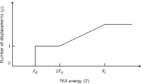
When an atom is detached from its lattice site, it could have considerable kinetic energy and travel through the lattice. This kind of atoms which are knocked out of the lattice are also called as knock-on atoms (or PKAs) and capable of producing secondary displacements. However, such a secondary displacement is produced by a hard sphere collision since the energy of PKAs is always lower than 𝐸𝐴. Kinchin and Pease have proposed a model [20] which describes the production of secondary displacements depending on the energy of PKAs, and today, this model is being widely accepted. A full Kinchin-Pease (K-P) result is presented as follow:
𝜌(𝑇) = 0 𝑇 < 𝐸𝑑 𝜌(𝑇) = 1 𝐸𝑑 ≤ 𝑇 < 2𝐸𝑑 𝜌(𝑇) = 𝑇 2𝐸𝑑 2𝐸𝑑 ≤ 𝑇 < 𝐸𝑐 𝜌(𝑇) = 𝐸𝑐 2𝐸𝑑 𝐸𝑐 ≤ 𝑇 (1-51)
where 𝐸𝑐 is the cut-off energy. It is assumed that the energy loss by electron stopping is given by this cut-off energy. If the PKA energy is greater than 𝐸𝑐, there is no more increase of generation rate of secondary displacements. The full curve describing K-P model is presented in Figure 1-6.
33
Figure 1-6. The number of displacement by the cascade as a function of PKA energy (from K-P model).
The average number of displacement, 𝜌̅, is obtained by taking an average of 𝜌 over the energy spectrum of the PKAs. In a form calculated by reference [13], 𝜌̅ is:
𝜌̅ =1 2( 𝑇𝑚 𝑇𝑚− 𝐸𝑑) (1 + 𝑙𝑛 𝑇𝑚 2𝐸𝑑) (1-52)
For particles that have energy greater than the threshold energy, the total number of an atomic displacement, 𝑁𝑑, can be described in terms of a displacement cross section, 𝜎𝑑, along with an average number of secondary displacements, 𝜌̅, induced by the primary displacement and the irradiation fluence, Φ as given in the relationship:
𝑁𝑑= 𝑛𝑎𝜎𝑑𝜌̅Φ (1-53)
where 𝑛𝑎 is the number of atoms per unit volume of a target absorber. By combining Eqs. (1-49) or (1-50) with Eqs. (1-52) and (1-53), it is possible to estimate the total number of displacement for an incident particle of energy 𝐸.
1.2.3 Ionization
When a target material receives an energy from incident particle, the energy received can remove electrons on the orbital from target atoms. This process is called as ionization. The Ionization process is the main cause of energy loss of charged particle travelling a target material. The absorbed radiation dose of incident particles is measured in Gy (J/kg, preferred SI unit). The calculation of absorbed dose units is started by considering a radiation through a slice of material which has a thickness of 𝑑𝑥. Then, the energy deposition at each slice of material (𝑑𝐸 𝑑𝑥⁄ ) is tabulated with respect to the kinetic energy
34
of incident particle. It is also called as stopping power. By multiplying radiation fluence, the formula for electrons and protons is obtained as below:
𝐷𝑜𝑠𝑒 (𝐺𝑦) = 1.6 × 10⁻⁶𝑑𝐸 𝑑𝑥(
𝑀𝑒𝑉 ∙ 𝑐𝑚2
𝑔 ) Φ(𝑐𝑚
−2) (1-54)
Note that the stopping power is a unique value for each material for each type of particle radiation. Thus, one must take into account to choose a proper value of stopping power. One of advantages of calculating the absorbed dose in Gy is that the conversion of absorbed dose between different particles (for example, between electron and proton).
The calculation programs of stopping power that has been developed by Berger et al [21] are available for most of solar cell materials. A program for electron computation is called as ESTAR, and for protons called as PSTAR, respectively.
1.3 Nature of irradiation-induced defects in solar cell materials
The study of defect is one of the most important problem in semiconductor physics. In crystalline or amorphous structure, the existence of defects can affect its electrical or optical properties in complex ways. Today, it is possible to theoretically predict a qualitative energy levels associated with some ideal simple intrinsic defects [22]. However, it is still not yet possible to qualitatively identify defects for the lattice distortion, and relaxation. To verify the theoretical prediction of defects, the experiments must be carried out to produce simple defects because tracking its mechanism after the production is already very complicated. The primarily created intrinsic defects, i.e. vacancies and interstitials are presumably moved out very fast and interact with other defects or impurities. Therefore, to irradiate with electrons is a proper choice to properly identify defects in a material. Then, once the defects are sufficiently identified, the comparison with proton irradiation result can be fulfilled. In this section, we collected and summarized some identified defects and their characteristics from the literature. We will discuss the production of defects and their behaviors in different kind of solar cell materials (GaAs, GaInP, and Ge) depending on the type of irradiation and temperatures. However, we have to keep in mind that the identified defects are limited as single defects, that is, complex of defects like cluster and their outcome property might not be measurable with modern measurement techniques. Furthermore, as we will mainly discuss below, most of defects that we are interested in for our study have been analyzed through either magnetic or electric way. So, we should be aware of that there could be still more veiled or non-identified defects by our irradiation conditions.

![Figure 2-12. EQE of the Ge sub-cell and component cell [4].](https://thumb-eu.123doks.com/thumbv2/123doknet/2833757.68704/72.892.202.692.709.1060/figure-eqe-ge-sub-cell-component-cell.webp)
