Pépite | Conception de circuits et systèmes avancés pour des applications de communications sans fil en gamme RF, mmW et THz
155
0
0
Texte intégral
(2) HDR de Andreia Cathelin Nitescu-Henry, Lille 1, 2013. Advanced circuits and systems for RF, mmW and THz wireless communications– HDR thesis. ACKNOWLEDGEMENTS I would first like to show my gratitude to professor Andreas Kaiser from IEMN, promoter of this work. Andreas has been first my microelectronics professor at ISEN, then my PhD advisor and finally road companion for a large majority of research activity developed jointly during the last 15 years, in the frame of the common laboratory ST-IEMN. And, of course, a great friend! Several other professors have been involved in most of the joint collaborative research. I warmly thank them for the great research that we lead together in a very productive and friendly atmosphere; they are, in order of appearance: François Danneville from IEMN Lille, Jean-Baptiste Begueret and Eric Kerhervé from IMS Bordeaux, Eric Tournier and Olivier Llopis from LAAS Toulouse, Christian Person from Lab-Stic Brest, Nathalie Rolland from IEMN, Ali Niknejad from UC Berkeley, Ullrich Pfeiffer from University of Wuppertal, Bram Nauta from University of Twente, Jan Rabaey and Bora Nikolic from UC Berkeley. Our former PhD students have boldly followed us and then found their own way, always hard working and with good humor. I as well warmly thank them for the nice cooperation we had: David Chamla, Stéphane Razafimandimby, Cyril Tilhac, Baudouin Martineau, Nicolas Seller, Jean Gorisse, Yenny Pinto, Romain Crunelle, Jonathan Muller, Mathieu Egot, Fawzi Houfaf, Hani Sherry; as well as those still on the way: David Borggreve, Camilo Salazar, and Dajana Danilovic. During all these years I have been empowered by the management of STMicroelectronics in Crolles, who has created the perfect environment for advanced R&D inside the company. I would like to address my gratitude to Philippe Magarshack, Executive VP of ST, and Dr. Pierre Dautriche, Director, who have shown their trust to my research activity and are supporting it. I am extremely grateful to the members of this habilitation jury. Professors Bram Nauta from University of Twente, Jan Rabaey from UC Berkeley and Paul-Alain Rolland from University of Lille have kindly accepted to report on this work. As well, thank you to the members of the jury: Dr. Pierre Dautriche from STMicroelectronics, professor Raymond Quéré from XLIM Limoges and professor Alain Cappy from IEMN. Thank you as well Alain for your trust and support during all these years of common lab! I would like to cite as well several colleagues from STMicroelectronics who are wonderful companions on the R&D path: Didier Belot, Frédéric Paillardet, Olivier Richard, Frédéric Gianesello, Stéphane Le Tual, Pratap Narayan Singh, Frédéric Hasbani, Philippe Flatresse, Christophe Garnier, Pierre Busson, Caroline Arnaud, Patrick Cogez as well as Pascale Maillet-Contoz and Nicolas Rolland; also former colleagues: Danilo Gerna, Carlo Tinella and Franck Badets. I would not be able to finish this list without naming four gentlemen now retired from ST who have taught me the dedicated and patient way of doing advanced R&D in industry: Ernesto Perea, Marcel Roche, Eugène Mackowiak and Jean-Pierre Schoellkopf. Last but not least, I would like to thank all my family for their support, with patience and lots of love and humor.. à Philippe et aux enfants, Emilie et Mircea. Andreia Cathelin. © 2014 Tous droits réservés.. May 2013. Page 3. doc.univ-lille1.fr.
(3) HDR de Andreia Cathelin Nitescu-Henry, Lille 1, 2013. Advanced circuits and systems for RF, mmW and THz wireless communications– HDR thesis. Soyons comme le chevalier Bayard: sans peur et sans reproches…. à Laval dans le Grésivaudan, le 6 mai 2013. Andreia Cathelin. © 2014 Tous droits réservés.. May 2013. Page 5. doc.univ-lille1.fr.
(4) HDR de Andreia Cathelin Nitescu-Henry, Lille 1, 2013. Advanced circuits and systems for RF, mmW and THz wireless communications– HDR thesis. TABLE OF CONTENTS I.. General Introduction ................................................................................................................... 9. II.. Analog integrated continuous time filters for wireless applications .................................. 11 II.1. Preamble .............................................................................................................................. 11. II.2. Reconfigurable filters for cellular applications .............................................................. 12. II.3. Filter tuning methodology for reconfigurable architectures ....................................... 23. II.4. Reconfigurable Gm-C filters with record cut-off frequency up to 10GHz ................ 36. II.5. Conclusions and perspectives .......................................................................................... 41. III.. BAW-IC co-integration for RF circuits ................................................................................ 43. III.1. Preamble .............................................................................................................................. 43. III.2. BAW technology ................................................................................................................ 44. III.3. BAW resonator filters ........................................................................................................ 47. III.4. Tunable BAW filters ............................................................................................................ 51. III.5. Tuning circuitry for BAW filters ...................................................................................... 58. III.6 Other co-integrated circuits using BAW devices: oscillators, phase noise integrated test-bench ........................................................................................................................................ 66 III.7 IV.. Conclusions and perspectives .......................................................................................... 76 mmW and THz design in deep submicron CMOS technologies .................................... 77. IV.1. Preamble .............................................................................................................................. 77. IV.2. Target applications in the mmW band............................................................................ 78. IV.3. Building a robust design methodology for mmW circuits in deep submicron CMOS 81. IV.4. Towards complex circuits and systems for mmW applications .................................. 94. IV.5. Conclusions and perspectives ........................................................................................ 128. V.. General Conclusion and perspectives ................................................................................... 129. VI.. Extended Curriculum Vitae ................................................................................................ 131. VI.1. Curriculum Vitae ............................................................................................................. 131. VI.2. Membership in conferences, reviewer, awards ........................................................... 134. VI.3. M.S. students supervision through industrial internship .......................................... 135. VI.4. Ph.D. students supervision (my supervision quota in bold blue) ................................... 136. VI.5. Participation to Ph.D. defense juries ............................................................................. 140. VI.6. Teaching activities (see also Invited talks in workshops/ seminars/ tutorials)................. 142. Andreia Cathelin. © 2014 Tous droits réservés.. May 2013. Page 7. doc.univ-lille1.fr.
(5) HDR de Andreia Cathelin Nitescu-Henry, Lille 1, 2013. Advanced circuits and systems for RF, mmW and THz wireless communications– HDR thesis. VI.7. Collaborative projects ...................................................................................................... 143. VI.8. Public Patents (as per Google Patents, on July 30, 2012) ............................................ 144. VI.9. Publications in peer-reviewed journals ........................................................................ 147. VI.10. Publications in peer-reviewed conferences with proceedings .............................. 149. VI.11. Invited talks in conferences with proceedings ......................................................... 156. VI.12. Invited talks in workshops/ seminars/ tutorials .................................................... 157. VI.13. Book chapters................................................................................................................ 158. VI.14. Workshop/ Seminar/ Short courses as organizer .................................................. 159. Andreia Cathelin. © 2014 Tous droits réservés.. May 2013. Page 8. doc.univ-lille1.fr.
(6) HDR de Andreia Cathelin Nitescu-Henry, Lille 1, 2013. Advanced circuits and systems for RF, mmW and THz wireless communications– HDR thesis. I. GENERAL INTRODUCTION This Habilitation Thesis manuscript presents some major results of the applied R&D work that I have conducted at STMicroelectronics since beginning of year 2000, and within a close collaboration with IEMN Lille. This research work has been supported by the numerous Cifre PhD thesis that I have been supervising as industrial advisor, the academic part being performed in most of the cases by Doctor Andreas Kaiser, Directeur de Recherche CNRS at IEMN. For several subjects, we have put in place a second academic supervision, like for example with UC Berkeley in California – professor Ali Niknejad, University of Twente in the Netherlands – professor Bram Nauta and University of Wuppertal – professor Ullrich Pfeiffer. The first big theme of my scientific research is focused on the design of integrated circuits and systems for wireless applications in the RF frequency bands. The first part is dedicated to the integration of continuous-time filtering solutions for 2-, 3and 4G mobile communications, work carried out in the early 2000 years. Given the large variety of standards to be addressed in the mobile terminals, it has come out as an interesting research topic to address analog base-band filtering solutions which are flexible and reconfigurable in terms of band pass, order, linearity and noise. Hence, several integrated circuits have been proposed using the Gm-C filtering technique, showing flexibility for GSM to W-CDMA standards requirements, in (Bi)CMOS 0.25 and 0.13µm. This kind of analog continuous time filters has been pushed to its utmost limit (CMOS 65nm), as we have then demonstrated its operation up to a record cut-of frequency of 10GHz. A systematic approach for the cut-off frequency tuning of such filters has been proposed as well as demonstrated experimentally. In a second part, this document presents the results of the research carried out on the potentialities of co-integration between BAW (Bulk Acoustic Wave) and Silicon traditional technologies, around year 2005. New perspectives in terms of circuits and systems have been opened for applications in the frequency bands below 10GHz. In the frame of a W-CDMA receiver, an innovative solution has been proposed for the replacement of external SAW filters with miniaturized co-integrated BAW-IC RF filters showing also electronically tuning capabilities. On a system level, in collaboration with LAAS in Toulouse, we have proposed a novel solution of fully integrated test-bench for phase noise measurements, based also on a co-integration between BAW and traditional IC technology. When used in a communication system, this integrated test-bench permits to dynamically adjust the system performance and hence power consumption, as a function of the environmental and ageing conditions. This concept represents an early implementation of the principle “Sense and React” which appears since only few years in most of the mobile communication systems showing low power features.. Andreia Cathelin. © 2014 Tous droits réservés.. May 2013. Page 9. doc.univ-lille1.fr.
(7) HDR de Andreia Cathelin Nitescu-Henry, Lille 1, 2013. Advanced circuits and systems for RF, mmW and THz wireless communications– HDR thesis. The second big theme addressed by my research brings solutions for the design of communication systems in the millimeter wave band, and at the end bringing an opening to THz imaging. The interest for high data-rate (Gb/s) wireless communications in the 60GHz frequency band and using fully integrated Silicon technologies has appeared middle of last decade. I have hence put in place a research activity in order to bring to life an industrially robust design methodology for millimeter wave systems using advanced (Bi)CMOS technologies. This expertise has then been used by an industrial design team from ST and CEA-Leti, to which I have participated, in order to propose one of the first fully integrated CMOS 65nm WirelessHD transceiver modules with integrated antenna and millimeter wave packaging solution. I have then conducted new research topics in order to propose alternative system architectures for such high data-rate applications, either in order to add more flexibility in the operation mode or to increase the energy efficiency towards mobile application usecases. Novel massively digital software defined radio transmitter architecture has been proposed for these Gb/s communications. In the same time, an alternative Local Oscillator based beam-forming solution has been studied, relying on Coupled Oscillators Array with Injection Locking capability. Finally, during the last few years, jointly lead with University of Wuppertal and IEMN, we have proposed fully integrated state of the art solutions for THz imaging using regular CMOS technology. For the very first time ever, a 65nm CMOS 1 k-pixel fully integrated camera has been proposed, able to detect and format signals in the frequency band from 650 to 1000GHz. The principle of self-mixing in the channel of a FET transistor is used to provide the detection of the THz signals. This major innovation in the field of integrated solutions for THz imaging opens new door for creating markets of miniaturized products for: detecting hidden metallic objects, monitoring the moisture level in the agriculture industry, nondestructive non-harmful imaging or spectroscopy in the biological domain and much more. Recently, this work has been acknowledged by the international scientific community with the 2012 STMicrolectronics Technology Council Innovation Prize and the 2013 ISSCC Jan Van Vessem Award for Outstanding European Paper. Since July 2012, the Imaging Division of STMicroelectronics has added the Silicon integrated THz technology to its product roadmap. All this work is presented in the three major chapters of this thesis. Each research topic has its own preamble, and conclusions and perspectives section. A large part of the technical details given in this manuscript are drawn from the major publications I have co-authored, such as JSSC or ISSCC papers.. Andreia Cathelin. © 2014 Tous droits réservés.. May 2013. Page 10. doc.univ-lille1.fr.
(8) HDR de Andreia Cathelin Nitescu-Henry, Lille 1, 2013. Advanced circuits and systems for RF, mmW and THz wireless communications– HDR thesis. II. ANALOG INTEGRATED CONTINUOUS TIME FILTERS FOR WIRELESS APPLICATIONS. II.1 PREAMBLE Early 2000, all around the world, all the major academic and industrial parties focused a large part of their research on multi-mode communication system for cellular applications. The 2, 3 and yet to come 4G standards had to co-exist, and hence a lot of research has started on reconfiguration ability of wireless transceivers. As well, it was the ending age of BiCMOS wireless transceivers and the opening era for the industrial full CMOS solutions. Under these circumstances, at STMicroelectronics we have as well decided to work on reconfigurable transceivers for applications such as GSM, DCS, W-CDMA. Inside this frame, I have started a research activity concerning the re-configurable analog integrated continuous time filters for such cellular applications, and we arrived under short time to the need for flexible and reconfigurable solutions. The research presented in this section has been carried out at STMicroelectronics with two trainee Master students, Laurent Fabre and Laurent Baud, in 2001 and respectively 2002, and was followed by a thorough research performed in collaboration with IEMN/ISEN, professor Andreas Kaiser, in the frame of the Cifre Ph.D. thesis of David Chamla, from 2002 to the end of 2005. The targeted applications were GSM to W-CDMA, with cut-off frequencies in the range of hundred of kHz up to few MHz. After a break of several years, we have decided to extend these analog filtering methods to very wide band applications for Gb/s data rate communications, such as IEEE 802. 15.3.c (Wi-HDMI or WiGig) for the wireless part, and high data rate optical wireline communications. In 2008-9 this research has been done internally at STMicroelectronics in collaboration with Romain Ferragut (cut-off frequency brought up to 1GHz). It was then continued after 2009 by a Cifre Ph.D. thesis, student Fawzi Houfaf, in collaboration with the University of Twente, professor Bram Nauta and IEMN/ISEN, professor Andreas Kaiser. This last topic brought us to the world record cut-off frequency of 10GHz ever attained for an analog continuous time low pass filter, published early 2012 at ISSCC.. Andreia Cathelin. © 2014 Tous droits réservés.. May 2013. Page 11. doc.univ-lille1.fr.
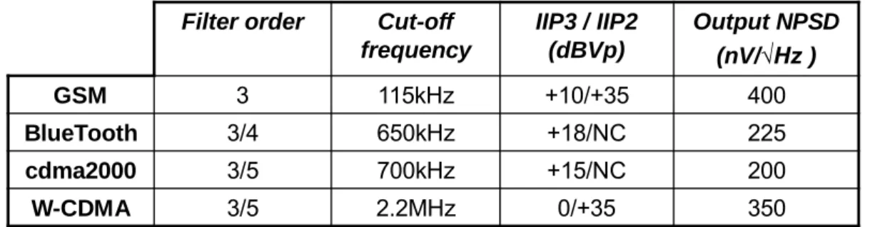
(9) HDR de Andreia Cathelin Nitescu-Henry, Lille 1, 2013. Advanced circuits and systems for RF, mmW and THz wireless communications– HDR thesis. II.2 RECONFIGURABLE FILTERS FOR CELLULAR APPLICATIONS The research presented in this section addresses the analog base-band section of a zero-IF architecture receiver, which was considered the best choice for such re-configurable cellular systems (see Figure II-1). We focus on the low-pass filter.. Figure II-1 Zero-IF receiver considered in this work When considering the major mobile communications standard for cellular, we rapidly can state the need for a wide tuning capability in the analog base-band filtering section. The table bellow illustrates this fact.. Table II-1 Major cellular standards bandwidth specifications System level research has determined the specifications needed for a reconfigurable analog base-band low-pass filter section, when considering several mobile applications specifications. These values are given in Table II-2, and they consist in the starting point for the research presented in this section. A Butterworth type of filter response function has been generally adopted for all the cases.. Andreia Cathelin. © 2014 Tous droits réservés.. May 2013. Page 12. doc.univ-lille1.fr.
(10) HDR de Andreia Cathelin Nitescu-Henry, Lille 1, 2013. Advanced circuits and systems for RF, mmW and THz wireless communications– HDR thesis. Filter order. Cut-off frequency. IIP3 / IIP2 (dBVp). Output NPSD (nV/√Hz ). GSM. 3. 115kHz. +10/+35. 400. BlueTooth. 3/4. 650kHz. +18/NC. 225. cdma2000. 3/5. 700kHz. +15/NC. 200. W-CDMA. 3/5. 2.2MHz. 0/+35. 350. Table II-2 General specifications for analog base-band filtering in zero or quasi-zero IF architectures for cellular applications We hence target a real-time filtering band-pass variation and reconfiguration, while a digital command is strongly recommended. Gm-C implementations of a ladder filter have been chosen, mainly because they provide low sensitivity to process variations, temperature drifts, and aging when associated with an on-chip automatic tuning system. Moreover, Gmtuning allows a perfectly continuous tuning over a wide frequency range. As well, a frequency tuning and tracking is needed for two reasons: -. Process, voltage, temperature (PVT) variations, as the cut-off frequency (fc) is allowed with only +/-5% variation We need the fc tracking over a wide frequency band. Two implementation examples of re-configurable low-pass filter aiming for the specifications given in Table II-2 are presented in the following subsections: -. Implementation example 1: fixed order filter with reconfigurable cut-off frequency Implementation example 2: variable order filter with reconfigurable cut-off frequency. II.2.1 IMPLEMENTATION EXAMPLE 1: FIXED ORDER FILTER WITH RECONFIGURABLE CUT-OFF FREQUENCY The largest cutoff frequency variation is given by GSM and W-CDMA cases (115 kHz and 2.1 MHz cutoff frequency respectively), hence imposing a cutoff frequency tuning ratio of around 20 [VI.9.2]. If process and temperature variations influences are taken into account, an fmax/fmin ratio of around 30 is needed. To extend the tuning range beyond the transconductor’s intrinsic tuning range, Gm-switching or capacitor-switching could be implemented. Gm-switching presents some important advantages compared to capacitorswitching. Indeed, with Gm-switching the maximum capacitance value is always used, thus maximizing the signal-to-noise ratio. Moreover, no switch has to be implemented on the signal path, so any issue relative to series resistance or switch linearity is avoided. Moreover, the proposed Gm-switching scheme keeps the parasitic capacitance constant on the signal nodes, making the layout implementation straightforward (Figure II-2).. Andreia Cathelin. © 2014 Tous droits réservés.. May 2013. Page 13. doc.univ-lille1.fr.
(11) HDR de Andreia Cathelin Nitescu-Henry, Lille 1, 2013. Advanced circuits and systems for RF, mmW and THz wireless communications– HDR thesis. A third-order Butterworth filter transfer function is implemented using an LC ladder network. If no capacitor switching is being used, the simple structure’s tuning ratio would be equal to that of a single transconductor and hence would have to be around 30. Unfortunately, one single transconductor can hardly provide this tuning range with satisfactory performances, especially in terms of linearity, noise, or power consumption. This led us to propose a multiple-Gm configuration structure, allowing a significant increase in the fmax/fmin ratio. In our case, two transconductor banks are connected in parallel to one single integration capacitor bank, so that the effective transconductance value is the sum of each of the transconductance cells. Within one transconductor bank, all of the transconductors present the same gm value.. Figure II-2 Multiple-Gm reconfigurable low-pass filter structure The proposed pattern consists of two transconductor banks (namely A and B ) connected in parallel, one of them (B) being switched on or off. Let be the maximum reachable ratio Gm_max/Gm_min for a single transconductor. We can then define the effective transconductance of this transconductor as :. √. √. (II-1). The first (always connected) transconductor bank A has an effective transconductance equal to Gm, and the second bank B consists of transconductors with an effective value of .Gm . When both banks are connected together to the same integration capacitors, the overall effective transconductance is (1+).Gm. Andreia Cathelin. © 2014 Tous droits réservés.. May 2013. Page 14. doc.univ-lille1.fr.
(12) HDR de Andreia Cathelin Nitescu-Henry, Lille 1, 2013. Advanced circuits and systems for RF, mmW and THz wireless communications– HDR thesis. The “Lower-Band” mode is defined as the tuning domain for which only bank A is connected, while the “Higher-Band” mode is defined as the tuning domain for which both A and B banks are connected to the integration capacitors. In order to maximize this structure’s transconductance tuning range, the highest attainable cutoff frequency in the Lower-Band should match the lowest cutoff frequency of the Higher-Band . Is this case, it can be easily seen that has to be =-1 . The fmax/fmin ratio of this structure has an effective tuning ratio that is equal to the transconductor tuning ability to a power of 2 (fmax/fmin = ²), whereas the total transconductance (thus current consumption) value has been multiplied by . In our case, a fmax/fmin ratio of 30 is needed. This means that the transconductor which has to be designed needs to achieve a transconductance tuning ratio of~6 (~30) . The transconductor cell implemented in this design is based on the one proposed by Alini et al. in IEEE JSSC, Dec. 1992, see Figure II-3.. Figure II-3 Tunable transconductor used in the first implementation example The MOS transistor is used in the triode regime, while the two bipolar transistors Q1 and Q2 are used to fix the drain voltage VB. Linearity performances are highly dependent on M1 and M2 VDS voltage because their large-signal transconductance is directly proportional to their VDS. As a result, the cascade transistor has to present the highest transconductance as possible to ensure that drain voltage remains practically constant despite large current variations. Bipolar transistors have been chosen here since they can provide a higher transconductance than MOS transistors for the same bias current. When looking at the noise performance, tradeoffs between noise and linearity become apparent. In the present design, the transconductor’s operating point is not changed by the tuning current except for transistors M1 and M2. The triode transistors’ VDS is tuned whereas their bias current remains constant. The tuning of the presented transconductor cell is realized through a parallel degeneration scheme with a simple controlled voltage sources connected between points A and B on the schematic.. Andreia Cathelin. © 2014 Tous droits réservés.. May 2013. Page 15. doc.univ-lille1.fr.
(13) HDR de Andreia Cathelin Nitescu-Henry, Lille 1, 2013. Advanced circuits and systems for RF, mmW and THz wireless communications– HDR thesis. It is clear that the noise/linearity tradeoff is one of the major design issues of this transconductor principle. Nonetheless, in the case of a necessary large tuning range, an optimal tradeoff is difficult to be found, since such a tradeoff is—per definition—only valid for a single operating point. The transconductor switching scheme introduced here limits the variation of the Gm , and eases the tradeoff. It can be said, though, that the noise-linearity tradeoff can be seen through the intermodulation-free dynamic range (IMFDR) value. The overall linearity of the transconductor decreases with VDS-M1,2 whereas the overall output noise decreases. The IMFDR is thus practically constant over the whole tuning range. In a multistandard application, it can be said that the linearity performances are above specifications, whereas noise performances would be below specifications, especially for cutoff frequencies at the lower end of each frequency range. As a result, a variable gain stage at the input of this filter should be able to minimize the input-referred noise, while remaining in the linearity specifications. The I and Q section of such low-pass filter for an analog base-bans section of a zero-IF receiver have been implemented in the 0.25µm SiGe BiCMOS process from STMicroelectronics, using also the 5fF/µm² MIM capacitors option, see Figure II-4.. Figure II-4 Die microphotograph of the 1st filter implementation (active area less than 0.5mm²) The tunability performance of this filter is presented in the following figure. While operating the filter in the lower band (A), the cut-off frequency can be linearly varied from ~50kHz up to 360kHz, while the higher band (A and B) permits to go from 250kHz up to 2.2MHz.. Andreia Cathelin. © 2014 Tous droits réservés.. May 2013. Page 16. doc.univ-lille1.fr.
(14) HDR de Andreia Cathelin Nitescu-Henry, Lille 1, 2013. Advanced circuits and systems for RF, mmW and THz wireless communications– HDR thesis. Figure II-5 Measured results of the 3rd order Butterworth tunable filter The other measured electrical parameters of this tunable filter are summarized in the next table.. Table II-3 Main measured electrical parameters The Gm-switching scheme applied to a tunable Gm–C low-pass filter presented here allows broadening the intrinsic tuning ability of a given transconductor. This kind of Gm-switching pattern permits designing analog baseband filtering stages in multistandard mobile communications systems. This system was implemented using a triode-based MOS differential pair as the core linear voltage-to-current converter, and was validated by designing a Butterworth low-pass filter in a 0.25µm SiGe BiCMOS process. Measurement results show very good accordance with specifications and simulation results. This Gmswitching principle is of course extendable to a larger number of transconductor banks. Finally, the circuit achieves a remarkably large tuning ratio of 1:40 and stands in good position with respect to state-of-the-art realizations.. Andreia Cathelin. © 2014 Tous droits réservés.. May 2013. Page 17. doc.univ-lille1.fr.
(15) HDR de Andreia Cathelin Nitescu-Henry, Lille 1, 2013. Advanced circuits and systems for RF, mmW and THz wireless communications– HDR thesis. II.2.2 IMPLEMENTATION EXAMPLE 2: VARIABLE ORDER FILTER WITH RECONFIGURABLE CUT-OFF FREQUENCY As specified in Table II-2, the numerous standards lying in the cellular band would request low-pass filtering section (in a zero-IF architecture) with a transfer function of the 3rd and often 5th order. In this second implementation, GSM and W-CDMA are chosen as well as corner-stones, as they represent the largest requested cut-off frequency span in a reconfigurable system [VI.9.4]. The specifications of this new circuit are the following: -. Within a Butterworth structure, present a switchable filter order of 3 or 5 Comply with the electrical specifications as per Table II-2 Minimize the power consumption and the occupied area. Because of its simplicity, an LC-ladder Gm -C implementation has been preferred over a biquad scheme. Moreover, such structures usually provide also improved sensitivity properties. Gm -C ladder topologies consist of input/output terminals and a chain of gyrators loaded by capacitors. Apart from the input and output terminations, such a topology can be considered as a series of basic structures consisting of two transconductors forming a gyrator, around which two grounded capacitors are connected, as depicted in Figure II-6 (refer to as the “basic cell”). In the general case, these capacitors are of different values, but the third-to-fifth order Butterworth configurability offers the possibility of a perfect symmetry, as shown in the next paragraph. In order to build the topologyconfigurable pattern, the highest-order structure is broken down into elementary basic cells, and some of these can be bypassed and turned off, allowing a reduction of power consumption for lower-order configurations. The values of the capacitors are deduced from the usual well-known synthesis methods. As an implementation example of this idea (see Figure II-7), let’s take the highest-order addressable topology as the starting point. The fifth-order Butterworth Gm-C implementation gives a {0.618; 1.618; 2; 1.618; 0.618} capacitor pattern, whereas the thirdorder Butterworth filter is synthesized with capacitor values of {1; 2; 1} [Figure II-7 (top)]. Sharing as much as possible capacitors between the third-order and fifth-order topologies leads to the implementation shown in Figure II-7(bottom). This technique here allows a 25% saving on capacitor area and power consumption and achieves a perfect symmetry in each of the basic cells. Although this technique is extendable to any topology, the third/fifthorder Butterworth configurability offers the best results in terms of area savings and symmetry.. Andreia Cathelin. © 2014 Tous droits réservés.. May 2013. Page 18. doc.univ-lille1.fr.
(16) HDR de Andreia Cathelin Nitescu-Henry, Lille 1, 2013. Advanced circuits and systems for RF, mmW and THz wireless communications– HDR thesis. L1. R1 C1. C1. R1. L1 C1. gm. -gm. -gm. -gm -gm. R1. gm gm. 1. 2. 1. L1 C2. C1. R1. gm. gm. gm. gm. -gm. -gm. -gm. -gm. -gm. gm -gm. 0.618. 1.618. 2. 1.618. 0.618. Figure II-6 LC ladder prototype and the equivalent Gm-C implementation for 3rd/5th order Butterworth low-pass filters. Figure II-7 Third/fifth-order switchable Butterworth Gm-C low-pass filter. (top) Basic configuration. (bottom) Optimized implementation Andreia Cathelin. © 2014 Tous droits réservés.. May 2013. Page 19. doc.univ-lille1.fr.
(17) HDR de Andreia Cathelin Nitescu-Henry, Lille 1, 2013. Advanced circuits and systems for RF, mmW and THz wireless communications– HDR thesis. In this implementation, it has been chosen to design a transconductor with a Gm tunability of about a factor of 25, in order to cover the full band from GSM to W-CDMA specifications. For tunability issues, the use of a transistor in its triode region has been again chosen; the schematic is depicted in Figure II-8. As in this operation region, the Gm value is directly proportional to the VDS value; being able to operate down to the lowest possible quiescent value for VDS becomes hence a necessity for a large tenability range.. Figure II-8 Principle of the proposed wide range tunable transconductor (half of the circuit is presented for readability purpose) However, simple circuits such as active cascode do not permit to control VDS down to zero. The employed technique is based on the principle introduced in J.L. Pennock et al., CICC 1986. Moreover, A. Zeki et al., Ell. Lett. 1999 introduces a control principle allowing to control down to zero which relies on matching. Of course, if a high precision is required on the cut-off frequency (consequently on the transconductance value), one cannot expect such a matching principle to achieve this requirement. Contrary to Zeki, the structure proposed here (depicted in Figure II-8) relies on the matching of two identical transistors instead of two transistors of different nature. M1 is, as stated before, operated in the triode region and acts as the voltage to current converter. M2 is the well known cascode transistor that reduces the voltage swing at VA ( M1’s VDS ). M4 transistors act as voltage-followers and M3 transistors provide voltage gain. The control voltage is input at the gate of M4b; at DC, M1’s VDS can be basically written as in (3) if the VGS ’s are perfectly matched: it can be seen that the VC vs VDS1 accuracy relies on the matching accuracy of transistors M3a and M3b on the one hand, and transistors M4a and M4b on the other hand. Good matching is realizable provided the circuit is properly and carefully laid-out, and provided the induced parasitic capacitances do not degrade the overall transfer function. Nonetheless, the overall matching performance is of course limited by the mismatch of M1’s transconductance factor µCox.(W/L) across the circuit. (II-2). The 3rd/5th order switchable order filter, tunable in frequency over 25X range, has been implemented using the previously presented transconductor in a 0.13µm CMOS process Andreia Cathelin. © 2014 Tous droits réservés.. May 2013. Page 20. doc.univ-lille1.fr.
(18) HDR de Andreia Cathelin Nitescu-Henry, Lille 1, 2013. Advanced circuits and systems for RF, mmW and THz wireless communications– HDR thesis. from STMicroelectronics. The chip comprises as well a novel topology of frequency tuning, which will be presented in the next sub-chapter.. Figure II-9 Chip photo-micrograph: the tunable filter and its Master-Slave tuning circuitry. The chip photomicrograph can be seen on Figure II-9. The total die area (with pads) is 1 mm² total, but the effective area is 0.57 mm². The measured transfer functions are depicted in Figure II-10, for four different cut-off frequencies in each mode (third/fifth order), and measured performances are summarized in Table II-4. On Figure II-10, the automatic tuning scheme has been bypassed, so as to account for the intrinsic filter performances. The implemented transconductor performances allow the cut-off frequency to be tuned from about 100 kHz to 2.75 MHz. Since the bias point of M1 (see Figure II-8) is modified when tuning the transconductor, linearity and noise performances vary accordingly. Indeed, the lower the transconductance value, the highest the input-referred noise power spectral density; this leads to very low noise (40 nV/Hz) for high cut-off frequencies, whereas the generated noise gets higher for very low VDS’s . As far as linearity is concerned, it degrades as VDS1gets closer to VDSsat .. Andreia Cathelin. © 2014 Tous droits réservés.. May 2013. Page 21. doc.univ-lille1.fr.
(19) HDR de Andreia Cathelin Nitescu-Henry, Lille 1, 2013. Advanced circuits and systems for RF, mmW and THz wireless communications– HDR thesis. Figure II-10 Measured transfer functions of the implemented switchable third/fifth order Butterworth tunable low-pass filter. Table II-4 Configurable Butterworth low-pass filter measured performance. Andreia Cathelin. © 2014 Tous droits réservés.. May 2013. Page 22. doc.univ-lille1.fr.
(20) HDR de Andreia Cathelin Nitescu-Henry, Lille 1, 2013. Advanced circuits and systems for RF, mmW and THz wireless communications– HDR thesis. The feasibility of a tunable and switchable-order Gm-C filter has been demonstrated in the context of a configurable Analog Baseband filtering stage for a zero-IF cellular receiver addressing common cellular standards such as GSM or W-CDMA. A technique suitable for the Gm -C ladder filter synthesis has been presented. This method allows to easily building a topology-configurable filter. Filter order and transfer function type can be programmed, either by the user or by software if included in a software-defined radio (SDR) radio scheme. A third/fifth-order Butterworth low-pass filter has been implemented using the presented technique and exhibits a tuning ratio above 25:1, with IIP3 around 10 dBVp and noise performances (down to 40 nV/Hz) allowing it to operate under the mentioned standards, for a maximum power consumption of 3.3 mW under 1.2-V operation, making it compatible with a GSM/W-CDMA configurability.. II.3 FILTER TUNING METHODOLOGY FOR RECONFIGURABLE ARCHITECTURES This section will give insights on automatic tuning methods for analog continuous time filters [VI.12.4]. The first part will present some general theoretical considerations, while the second part will present a novel automatic tuning method and its Silicon implementation as tuning circuitry for the filter presented in example 2.. II.3.1 THEORETICAL ASPECTS OF FILTER TUNING The cut-off frequency of an analog filter is a function of a time constant; for example, for a Gm-C filter: (II-3). Any part of an integrated circuit suffers from process, voltage and temperature (PVT) variations. These variations are very important: . Process variations (including ageing): . . Voltage variations: . . Gm ± 30%, R ± 20%, C ± 20% (generally uncorrelated). Vdd ± 5 or 10%. Temperature variations: . General industrial range: -35 … 80°C. When taking all this data into account, we end up with a global filter cut-off frequency variation of roughly ±50%. Andreia Cathelin. © 2014 Tous droits réservés.. May 2013. Page 23. doc.univ-lille1.fr.
(21) HDR de Andreia Cathelin Nitescu-Henry, Lille 1, 2013. Advanced circuits and systems for RF, mmW and THz wireless communications– HDR thesis. On the other hand, the system specifications for example in a wireless transceiver generally tolerate a variation of the cut-off frequency of only ±5%. It becomes hence obvious that the full filtering zone needs to be served by a cut-off frequency tuning circuitry. Sometimes, if stringent specifications on in-band ripple apply, a quality factor tuning circuitry may be needed as well. The general idea of the tuning methodology can be simply sketched by the following needs: . Provide the system with an external reference value (e.g. clock frequency, voltage reference, well-known value passive component-resistor, capacitor). . Build a tuning/comparison circuitry which has an (external) absolute reference value, locked into a loop. . Control the filter with an electrical (analog/digital) command:. . . Current. . Voltage. . Digital word. The control command may be: . Permanent. . Periodical. . On demand. . At power-up (trimming). . At circuit final test (trimming). . At final product manufacturing (trimming). The tuning methodology can then be thought into two big families: direct and indirect tuning. The next principle schematics and tables sum-up these methods and provide the major advantages and drawbacks.. Andreia Cathelin. © 2014 Tous droits réservés.. May 2013. Page 24. doc.univ-lille1.fr.
(22) HDR de Andreia Cathelin Nitescu-Henry, Lille 1, 2013. Advanced circuits and systems for RF, mmW and THz wireless communications– HDR thesis. IN. (1). OUT. (1). FILTER. (2). (2). HOLD comparison CLOCK Advantages. Drawbacks. Accurate tuning method. Long settling time Discontinuous filtering capability. Figure II-11 Direct tuning (I): sampled tuning method. (1). (1). FILTER A. (2). (2). HOLD. IN. OUT. Vcomp. (1). (1). FILTER B. (2). (2). HOLD Vcomp. comparison CLOCK. Advantages. Drawbacks. Accurate tuning method (but need matching between A and B) Continuous filtering capability. Long settling time (IIR filter) Large circuit area and complexity. Figure II-12 Direct tuning (II): continuous tuning method The drawbacks of the direct tuning methods make them not very useful in the case of analog base-band filters for wireless transceivers. For this use case, the preferred method is the indirect tuning, which will be detailed in the following paragraphs. Andreia Cathelin. © 2014 Tous droits réservés.. May 2013. Page 25. doc.univ-lille1.fr.
(23) HDR de Andreia Cathelin Nitescu-Henry, Lille 1, 2013. Advanced circuits and systems for RF, mmW and THz wireless communications– HDR thesis. The indirect tuning method can be explained using the Master-Slave technique. . The External reference is, as in the previous cases, a CLOCK frequency.. . The System SLAVE is the filter to be tuned: . . E.g., its cut-off frequency is :. The System MASTER is a circuit which has a representative frequency given by the same elements as the SLAVE: . E.g. 1: a filter with the cut-off frequency given by:. (or homothetic) =>. in this case, we are talking about a Frequency Locked Loop (FLL) system . E.g. 2: a VCO with its oscillation frequency given by:. (or homothetic). => in this case, we are talking about a phase locked loop (PLL) system . The COMPARISON CIRCUIT locks the MASTER behavior to the External reference. . The COMMAND VALUE controls in the same time the MASTER and the SLAVE. Hence, the SLAVE circuit which is the element to be tuned is indirectly indexed on the External Reference element. IN. FILTER (SLAVE). OUT. FILTER (MASTER). COMPARISON. Vcommand. CLOCK. Advantages. Drawbacks. Continuous time tuning Continuous filtering capability. MASTER and SLAVE matching may be limited by the Silicon technology matching features. Figure II-13 Indirect tuning scheme, FLL type. Andreia Cathelin. © 2014 Tous droits réservés.. May 2013. Page 26. doc.univ-lille1.fr.
(24) HDR de Andreia Cathelin Nitescu-Henry, Lille 1, 2013. Advanced circuits and systems for RF, mmW and THz wireless communications– HDR thesis. IN. FILTER (SLAVE). OUT. OSCILLATOR (MASTER). COMPARISON. Vcommand. CLOCK. Advantages. Drawbacks. Continuous time tuning Continuous filtering capability The PLL might be used for some reference frequency generation on the chip. MASTER and SLAVE matching may be limited by the Silicon technology matching features The MASTER oscillator may become an undesired frequency on the chip (possible coupling issues). Figure II-14 Indirect tuning scheme, PLL type In the case of an indirect tuning using either the PLL or the FLL type (see Figure II-13 and Figure II-14), the tuning condition is that the MASTER (M) and SLAVE (S) are to be matched either: . Directly (e.g. gm_M = gm_S and C_M = C_S) or. . Homothetic (e.g. gm_M = gm_S/N and C_M = C_S/P), where N and P are constants. Several classical examples of indirect tuning schemes will be now presented.. Andreia Cathelin. © 2014 Tous droits réservés.. May 2013. Page 27. doc.univ-lille1.fr.
(25) HDR de Andreia Cathelin Nitescu-Henry, Lille 1, 2013. Advanced circuits and systems for RF, mmW and THz wireless communications– HDR thesis. II.3.2 CUT-OFF FREQUENCY TUNING USING THE FLL SOLUTION In this case, the MASTER is a low-pass 2nd order filter. The CLOCK signal is fed on two pathes: a direct one and another one by the MASTER, the two signals are then voltage limited and compared in terms of phase through a XOR type of circuitry. A homothety bloc may be needed if the MASTER and SLAVE are scaled homothetically. FILTER (SLAVE). IN. OUT. Homothety bloc Loop filter MASTER (LP filter) CLOCK. XOR. Figure II-15 Cut-off frequency indirect tuning, FLL solution In order to insure the tuning system accuracy at the phase detector level, the designer has to take into account: . Amplitude mismatches: . . Structure insensitive (1st order), use of voltage limiters. Phase mismatches: . Any phase offset at the XOR input generates a systematic error on the command voltage. The Use of a Qp>1 in the MASTER for steep phase rotation makes it less sensitive to phase variations. The tuning accuracy at the command value level implies a deep study of the Homothety bloc in order to predict and if possible avoid/compensate for the systematic errors.. Andreia Cathelin. © 2014 Tous droits réservés.. May 2013. Page 28. doc.univ-lille1.fr.
(26) HDR de Andreia Cathelin Nitescu-Henry, Lille 1, 2013. Advanced circuits and systems for RF, mmW and THz wireless communications– HDR thesis. II.3.3 CUT-OFF FREQUENCY TUNING USING THE PLL SOLUTION In this case the tuning system accuracy at the loop level has no dependency (at 1 st level) on the accuracy of the phase-frequency detector (PFD). The major problem here is to insure a good quality controlled oscillator.. IN. CLOCK. SLAVE (filter). OUT. PD. ChP. ÷N. Homothety bloc Loop filter. MASTER (VCO). Figure II-16 Cut-off frequency indirect tuning, PLL solution An example of a Gm-C VCO to be used as a MASTER in this kind of structure is presented in Figure II-17.. Figure II-17 Gm-C VCO; may be used as MASTER in the indirect PLL tuning solution The negative (Rneg) and positive (Rpos) resistor-like circuitry is needed in order to limit the output amplitude. An easy way to obtain this kind of circuitry is by using a Gm and a –Gm respectively in a feedback mode loop. The Rneg is of course compensating for the LCequivalent tank losses. The Rpos should be much smaller than the parasitic output resistance of the LC-equivalent tank, hence the output conductance is dominated by 1/Rpos, permitting a better control of the output conductance. Finally, the harmonic oscillation conditions (see also Figure II-18) are met if: . Rpos is degenerated. . |Rpos| > |Rneg|. Andreia Cathelin. © 2014 Tous droits réservés.. May 2013. Page 29. doc.univ-lille1.fr.
(27) HDR de Andreia Cathelin Nitescu-Henry, Lille 1, 2013. Advanced circuits and systems for RF, mmW and THz wireless communications– HDR thesis. iout 1/Rpos total Vin. 1/Rneg A. Figure II-18 Oscillation stabilization principle for the Gm-C VCO. II.3.4 QUALITY FACTOR TUNING CIRCUITRY USING AN ALL SOLUTION A major problem that can be encountered in Gm-C filters is that the secondary poles in individual Gm’s may cause variation (deterioration) in the overall filter quality factor Q. regularly, as a rule of the thumb, we may consider that a secondary transconductor pole will not “bother” the filter quality factor if f_2ndPole>102.fc. If the chosen technology process cannot afford for this two decades margin, then the designer has to go for a Q-tuning circuitry. Figure II-19 presents such a solution based on an Amplitude Locked Loop (ALL), where we use a filter with homothetic or identical Gm structures as the one to be tuned and then tune the position of all the secondary poles.. IN. SLAVE (filter) Homothety bloc. Frequency reference (Ao, fo). OUT. Vcontrol_Q. Loop filter. MASTER (BP filter). +. Figure II-19 Q-factor indirect tuning, ALL solution In this case the external reference is now a Frequency Reference with known values for (Ao, fo). The MASTER is generally a band-pass filter identical / homothetic to the SLAVE filter (in general: fc_SLAVE=fcenter_MASTER) and has a unitary gain. The amplitude detectors absolute figures are compensated (at 1st order) by the subtraction circuitry. The same considerations as for the other indirect tuning methods apply for the homothety bloc.. Andreia Cathelin. © 2014 Tous droits réservés.. May 2013. Page 30. doc.univ-lille1.fr.
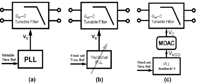
(28) HDR de Andreia Cathelin Nitescu-Henry, Lille 1, 2013. Advanced circuits and systems for RF, mmW and THz wireless communications– HDR thesis. II.3.5 IMPLEMENTATION EXAMPLE OF A FILTER FREQUENCY TUNING AND TRACKING CIRCUITRY FOR MULTI - MODE TRANSCEIVERS We reconsider the case of multi-mode wireless transceivers for cellular communications, and we focus again on the base-band filtering section in the case of a zero-IF architecture. The reconfigurable filters architecture presented earlier in this subchapter present a cut-off frequency tunable over a factor of 25 (100kHz to 2.75MHz) in order to cover most of the standards (see filter implementation example number 2, [VI.9.4]). Using a regular PLL type indirect tuning scheme would imply to generate somehow as many reference frequencies as standards to be supplied (see Figure II-20, a). Furthermore, the main reference clock frequency in communication standards is not related to the channel spacing, making the reference frequency generation a tricky issue.. Figure II-20 Different ways of locking a PLL Master-Slave tuning circuitry As an alternative, one could seek to lock the PLL to a fixed reference and make the PLL programmable as depicted in Figure II-20(b). However, the large range of cut-off frequencies that need to be covered make the PLL design very challenging. Finally one could try to make the frequency tracking between the PLL and the filter programmable by inserting a programmable voltage divider between the PLL and the filter as shown in Figure II-20(c). A very simple PLL (unity feedback loop) could then be used with a fixed reference frequency, and a programmable divider adjusts the cut-off frequency of the filter relative to the reference frequency. But the nonlinear behavior of the Gm versus control voltage relation would naturally lead to errors on the actual transconductance ratio as shown in Figure II-21 for the particular case where fVCO is programmed to be 4*ffilter. Therefore, a simple scheme as in Figure II-20(c) cannot in general provide accurate results.. Andreia Cathelin. © 2014 Tous droits réservés.. May 2013. Page 31. doc.univ-lille1.fr.
(29) HDR de Andreia Cathelin Nitescu-Henry, Lille 1, 2013. Advanced circuits and systems for RF, mmW and THz wireless communications– HDR thesis. Figure II-21 Error mechanism of linear transconductance control We hence proposed to use a transconductance division scheme that accurately links the filter control voltage VC to the PLL control voltage VVCO. The circuit fixes the actual Gm ratio to match the desired ratio fVCO/ffilter by a transconductance division scheme.. Figure II-22 Implementation of the accurate G ratio division The principle of the circuit is shown in Figure II-22. It comprises two transconductors, Gm1 and Gm2 , and a control loop. Gm1 is matched to the transconductance of the VCO, Gm2 to the transconductances used in the filter. An arbitrary DC voltage v2 is used as an input to Gm2 , while a voltage equal to v2/N is fed to the input of Gm1 . If the two output currents Andreia Cathelin. © 2014 Tous droits réservés.. May 2013. Page 32. doc.univ-lille1.fr.
(30) HDR de Andreia Cathelin Nitescu-Henry, Lille 1, 2013. Advanced circuits and systems for RF, mmW and THz wireless communications– HDR thesis. of the transconductors ( i1 and i2, respectively) are made equal by the control loop, then the ratio between Gm1 and Gm2 is obviously determined by the ratio between v1 and v2; see the equations below. i1 = Gm1.v1. (II-4). i2 = Gm2.v2. (II-5). if N =v2/v1 and if i1 = i2, then Gm1/Gm2 = N. (II-6). This way, a voltage division of factor N (through a simple potentiometer or a digital-toanalog converter) precisely sets the ratio between Gm1 and Gm2. The main constraints affecting this system’s accuracy are offsets and the variations as a function of input levels. Both these constraints can become troublesome with large attenuation factors (N). Indeed, in the presented application, a 10-bit multiplying-DAC (MDAC) has been used to implement the attenuation factor N. When reaching its highest value, v2/N still needs to remain much higher than the offsets. This tuning scheme allows to use transconductors of different structure in the VCO and in the filter. Indeed, the Gm–division scheme ensures that the ratio Gm1/Gm2 is properly fixed, regardless of the transconductors implementations. This can be suitable when the respective operating frequencies of the master and slave circuits are very different. However, GM1 has to be matched to the transconductors of the VCO while Gm2 needs to be matched to the transconductors of the filter. The proposed master/slave tuning architecture has been implemented with the widely tunable third/fifth-order Butterworth low-pass filter presented before in the 0.13µm CMOS process. The chip partitioning (see Figure II-9) shows that the master/slave scheme (“PLL” and “Gm div.” parts) area is small when compared to the filter area (“Gm ’s” and “Capacitors matrix” parts): the tuning circuit area is 0.09 mm² for a total area of 0.55 mm² . The complete proposed master/slave architecture is illustrated in Figure II-23. Shaded boxes indicate which parts of the architecture have actually been integrated on-chip. We have chosen to use a commercially available high-performance DAC on our test-board to evaluate our architecture’s performances. The DAC voltage reference is generated on-chip and both resulting differential DC voltages are connected to Gm1 and Gm2 differential inputs. The master/slave scheme is intended to function in a way that the PLL operates at a frequency placed out of the filter’s pass band, so as to avoid parasitic signals in the concerned channel.. Andreia Cathelin. © 2014 Tous droits réservés.. May 2013. Page 33. doc.univ-lille1.fr.
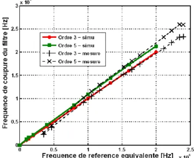
(31) HDR de Andreia Cathelin Nitescu-Henry, Lille 1, 2013. Advanced circuits and systems for RF, mmW and THz wireless communications– HDR thesis. Figure II-23 Proposed master/slave architecture (actual integrated parts are shaded). Since the application is aimed at addressing cellular standards from GSM to W-CDMA (cutoff frequencies from about 100 kHz to 2.5 MHz, respectively), the PLL operates slightly above 2.5 MHz. Measurements were made to quantify the master/slave architecture efficiency. This has been done by tuning the DAC’s division ratio (controlled by a 10-bit word) and by measuring the actual filter’s cut-off frequency. It is possible to display these results as shown on Figure II-24.. Figure II-24 Measured filter cut-off frequency as a function of the equivalent reference frequency (fref_eq = fref/N). It can be seen that the overall matching is very good (less than 5% error) from about 500 kHz to the upper tuning limit (validated from 30 C to 80 C, with 10% supply variations, as seen on Figure II-25), and that a very good agreement between measurements and simulations can be reported. The settling time of the control loop has been simulated to be less than 15 µs. The tuning circuit power consumption is less than 500 µW (value at fref=2.5 MHz).. Andreia Cathelin. © 2014 Tous droits réservés.. May 2013. Page 34. doc.univ-lille1.fr.
(32) HDR de Andreia Cathelin Nitescu-Henry, Lille 1, 2013. Advanced circuits and systems for RF, mmW and THz wireless communications– HDR thesis. Figure II-25 Measured filter response with tuning circuitry ON for several temperatures. An indirect PLL based master/slave technique which allows to digitally tune a Gm -C filter’s cut-off frequency with respect to a single available reference clock has been proposed. This system is aimed at addressing widely-tunable filters in the context of analog baseband circuits for multi-standard configurable receivers. Instead of relying on the sometimes complex PLL tunability, the whole flexibility has been moved to the proposed master/slave scheme, which consists of a transconductance division. The feasibility of this concept has been proven to work by implementing the automatic tuning system of a classical Gm -C third/fifth-order Butterworth low-pass filter, in a standard 0.13µm 1.2-V CMOS process.. Andreia Cathelin. © 2014 Tous droits réservés.. May 2013. Page 35. doc.univ-lille1.fr.
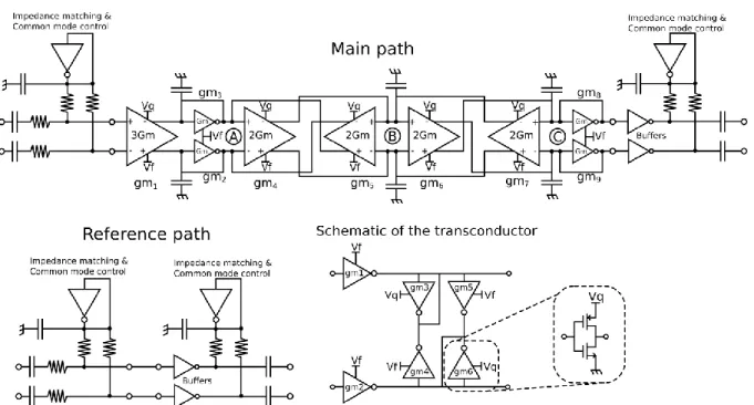
(33) HDR de Andreia Cathelin Nitescu-Henry, Lille 1, 2013. Advanced circuits and systems for RF, mmW and THz wireless communications– HDR thesis. II.4 RECONFIGURABLE GM-C FILTERS WITH RECORD CUT-OFF FREQUENCY UP TO 10GHZ Since several years Analog and RF designers face the race towards the ultimate highest data rate, for wireless as well as for wireline communications. The 60GHz high-data rate standards as well as the optical links are good examples in this field. Hence, at the end of the day, the analog designer will have to cope with a signal of 1 or more GHz band that has to be filtered to avoid anti-aliasing or the effects of blockers or other unwanted signals. Active filters are hence interesting given their size (area cost as well) and offer interesting band flexibility capabilities. The state of the art early 2012 shows fully integrated solutions in CMOS operating at 1.7GHz and in BiCMOS at 3GHz. End 2009, we hence targeted to implement a tunable low-pass active filter with cut-off frequencies going from below 1GHz up to 10GHz, in a 65nm LP CMOS process [VI.10.66]. The Gm-C technique imposes itself as the only viable filtering implementation in order to target the 10GHz cut-off frequencies. As well, it shows very straightforward wide frequency range tunability capabilities. The implementation was focused on a 3rd order low-pass Chebyshev topology, implemented upon the LC-ladder synthesis method in order to take benefit of its low sensitivity to parameters variations (see Figure II-26). The LC-ladder prototype is then transformed into a Gm-C prototype with unitary transconductance Gmcells and scaled capacitors. For gain purpose and in order to increase the linearity on the internal node B, some transconductors are scaled up to 2X or even 3X. To facilitate measurements, the filter has been normalized on 100 Ohm differential impedance.. Figure II-26 Reconfigurable Gm-C filter for operation up to 10GHz (main path schematic, reference path schematic and transconductor electrical schematic). Andreia Cathelin. © 2014 Tous droits réservés.. May 2013. Page 36. doc.univ-lille1.fr.
(34) HDR de Andreia Cathelin Nitescu-Henry, Lille 1, 2013. Advanced circuits and systems for RF, mmW and THz wireless communications– HDR thesis. System level simulations have provided specifications for the unitary Gm-C integrators, in order to obtain an active filter with the same frequency behavior as the passive LC prototype. They need to show a DC gain over 30dB and a non-dominant pole above 300GHz, while the physical implementation is performed in a technology with a transition frequency fT of 160GHz for the intrinsic NMOS transistors. This extreme (we may even say ultimate) challenge can be fulfilled only with the simplest possible transconductor implementation, which is the CMOS inverter (“A CMOS transconductance-C filter technique for very high frequencies”, Nauta, B., Solid-State Circuits, IEEE Journal of , Volume: 27 , Issue: 2, 1992 , Page(s): 142 - 153), operated in a pseudo-differential scheme (transconductors gm1 and gm2 in Figure II-26). This solution presents no internal nodes, hence facilitating the high operation bandwidth. The implementation shows low impedance for the common mode and a high impedance for the differential one, hence enhancing the DC gain value. Extra transconductors are used between the differential output nodes in order to ensure the CM stability and to compensate for the finite output conductance of the structure. A careful electrical simulation study has been performed on the sizes of these 4 transconductors (gm3-6) in order to ensure the CM stability and the DC gain maximization while showing the minimum possible loading parasitic capacitance. In terms of layout physical implementation, a huge effort has been performed as well. First of all, as this filter is meant to deal with quite large power consumption, special care has been taken in order to be compliant with the ElectroMigration rules down to the tiny transistor fingers. Then, in terms of ElectroMagnetic parasitic effects: -. -. -. The parasitic resistive elements affect directly the insertion losses and destroy the ideal filter quality factor. In order to cope with this, the layout strategy was to employ large tracks and metal stacking The parasitic inductive effects spoil the filter transfer function shape in the stopband. The layout strategy in this case imposed that for each CMOS inverter; a layout distribution like PMOS-NMOS-PMOS-NMOS-PMOS is adopted, using unitary transistors of equal “height”. As well, a millimeter-wave style ground shielding strategy has been implemented. The capacitive effects limit directly the maximum achievable filter cut-off frequency. It has hence been decided to work only with parasitic capacitors for the integration nodes.. All these elements imply an extremely careful EM circuit layout analysis using 2D EM simulation tools. The filter core layout view is depicted in Figure II-27, showing how this millimeter-wave layout strategy has been deployed into an analog-style schematic.. Andreia Cathelin. © 2014 Tous droits réservés.. May 2013. Page 37. doc.univ-lille1.fr.
(35) HDR de Andreia Cathelin Nitescu-Henry, Lille 1, 2013. Advanced circuits and systems for RF, mmW and THz wireless communications– HDR thesis. Figure II-27 Filter core layout for operation up to 10GHz. For testability issues, a main signal path has been implemented aside a reference path, as presented in Figure II-26 and Figure II-28.. Figure II-28 Chip photomicrograph, 65nm LP CMOS process. Andreia Cathelin. © 2014 Tous droits réservés.. May 2013. Page 38. doc.univ-lille1.fr.
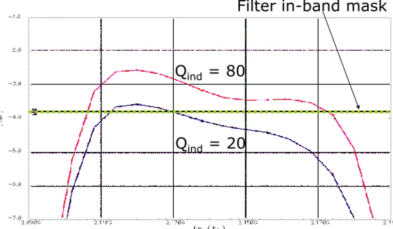
(36) HDR de Andreia Cathelin Nitescu-Henry, Lille 1, 2013. Advanced circuits and systems for RF, mmW and THz wireless communications– HDR thesis. The filter measured performance presents amazing performances fully in line with the electrical and electro-magnetic simulations.. Figure II-29 Measured S parameters for the 500MHz – 10GHz reconfigurable Gm-C filter Measurements show S-parameters which correspond exactly to the ideal passive LC prototype (see Figure II-29). The Q-tuning was performed manually, it shows 1dB gain, 1.2 dB ripple, a notch was observed at around 8 times the cutoff frequency probably due to a coupling between signal lines via dummy fillers which had not been completely extracted. Varying Vf shows a large tuning range from 0.6 to 10GHz. The IIP3 measurements are reported for edge of the band signal tones (25MHz spacing), while the noise measurements are performed over the filter pass-band using wide-band instrumentation amplifier at the output. All the presented figures are de-embedded of the input and output access elements thanks to additional measurements on the reference path. The obtained measured performance in terms of noise and linearity, even at the record cutoff frequency of 10GHz, outperforms the existing state of the art. The generic power per pole per Hz figure of merit permits to compare the different implementations, see Table II-5. For the same energy efficiency as the work presented in P. Wambacq et al., ESSCIRC 2010, the presented work exhibits ~5 times larger cut-off frequency for the same noise behavior and an edge of band IIP3 15dBc better. From an applicative perspective, in the case of 10GHz HDR optical links, a SNR of 36dB is requested while the presented work out-performs with a margin of 9dB. This work has demonstrated the feasibility and robustness of up to 10GHz low-pass continuous time filters in deep submicron CMOS process, with excellent noise and linearity behavior and with a continuous cut-off frequency tuning capability of over a decade. The transconductor solution proposed by Nauta in 1989 and implemented in a 3µm CMOS technology for a filter working at 100MHz translates 25 years later into a 65nm CMOS lowAndreia Cathelin. © 2014 Tous droits réservés.. May 2013. Page 39. doc.univ-lille1.fr.
(37) HDR de Andreia Cathelin Nitescu-Henry, Lille 1, 2013. Advanced circuits and systems for RF, mmW and THz wireless communications– HDR thesis. pass filter working at 10GHz! This implementation is as of today world record in terms of extremely high cut-off frequency integrated continuous-time low pass filters.. Table II-5 Performance of the Gm-C filter configurable up to 10 GHz and comparison with state of the art (for detailed references index in the Table, see ref [VI.10.66]). Andreia Cathelin. © 2014 Tous droits réservés.. May 2013. Page 40. doc.univ-lille1.fr.
(38) HDR de Andreia Cathelin Nitescu-Henry, Lille 1, 2013. Advanced circuits and systems for RF, mmW and THz wireless communications– HDR thesis. II.5 CONCLUSIONS AND PERSPECTIVES This section has been dedicated to the research in the field of tunable and adjustable continuous-time analog filters, for bandwidths spanning from hundred kHz up to tenths of MHz and finally extended to GHz. This research has accompanied the race for flexibility in transceivers for cellular mobile applications, and then spanning for larger data rate communication systems, for both Wireless and Wireline applications. As well, a methodology for frequency tuning of high frequency span analog filters has been presented and illustrated with circuit implementation. The Gm-C filter architecture has been chosen in all the cases, as it is well recognized as the most flexible to bandwidth changes, while presenting the least dependence to parameters sensitivity. Very simple but smart transconductor topologies have been chosen in order to ensure enough system linearity, while minimizing parasitic elements. This research has been declined in technology nodes from BiCMOS 0.25µm down to 65nm CMOS. The race towards the highest possible operation frequency brought us to a world record in the cut-off frequency of an analog filter, 10GHz, which implied the usage of the simplest possible transconductor topology and the design with millimeter wave considerations. The simplest possible transconductor being the CMOS inverter, as predicted and demonstrated by professor Nauta some 25 years ago. Hence, the future in this field is to be made with solutions from the past, meaning that the CMOS technology scaling will provide useful design margin to analog base-band filtering sections, especially if the basic building brick is the CMOS inverter.. Andreia Cathelin. © 2014 Tous droits réservés.. May 2013. Page 41. doc.univ-lille1.fr.
(39) HDR de Andreia Cathelin Nitescu-Henry, Lille 1, 2013. Advanced circuits and systems for RF, mmW and THz wireless communications– HDR thesis. III. BAW-IC CO-INTEGRATION FOR RF CIRCUITS III.1 PREAMBLE Early 2000 at STMicroelectronics, research in the field of piezoelectric devices suited for integration in modern Silicon technologies has drawn to Bulk Acoustic Wave (BAW) devices. BAW devices are piezoelectric resonators working in the frequency range from 1 to 10GHz and typically showing quality factors of about 1000. One of the potential advantages of such a technology is the compatibility of the BAW process with standard silicon industrial manufacturing, thus above IC co-integration may be foreseen in some cases. The regular IC process is hence enriched with a kind of “low quality reference resonators” (when compared for example to Quartz resonators), but with the unexpected possibility of intimate cointegration. Starting from this point, a new playground is opened to the analog and RF designer, and novel system architectures can be invented with this newly created perimeter. Inside a design research team at STMicroelectronics in Crolles, from 2002 to around 2010, I have been in charge of a small team working on BAW-IC co-integration design solutions for mobile communications applications. We have addressed several design fields: starting from electrically tunable BAW-based filters and their tuning methodology, then working on BAW-based oscillators and finally proposing novel system architectures. The internal design research has been done in a very tight collaboration with the process teams from STMicroelectronics and CEA-LETI. The pure design part of the activity has been done mainly in the frame of Cifre and lab PhD thesis in collaboration with: . . IEMN-ISEN Lille (professor Andreas Kaiser, student Stéphane Razafimandimby) and XLIM Limoges (professor Valérie Madrangéas, student Cyril Tilhac) for the filter design and LAAS Toulouse (professors Olivier Llopis and Eric Tournier, student Sylvain Godet) for the integrated phase-noise measurement test-bench; as well as in the frame of an FP7 EU-funded project called Mobilis.. After a short introduction, the major part of this research will be explained in the following sections.. Andreia Cathelin. © 2014 Tous droits réservés.. May 2013. Page 43. doc.univ-lille1.fr.
(40) HDR de Andreia Cathelin Nitescu-Henry, Lille 1, 2013. Advanced circuits and systems for RF, mmW and THz wireless communications– HDR thesis. III.2 BAW TECHNOLOGY III.2.1 BAW RESONATORS BAW resonators are typically composed of 3 parts: the electrodes, a piezoelectric layer and an isolation part [VI.13.2]. The isolation is obtained with an air gap for TFBAR (Thin Film Bulk Acoustic Resonator) and with a Bragg reflector for SMR (Solidly Mounted Resonator) (see Figure III-1). The principle of the isolation part is that a change in the impedance affects the amount of acoustic energy that is reflected and transmitted. Creating a discontinuity at material boundaries allows breaking the transmission of an acoustic wave in the materials. Hence, Bragg mirror consists of several pairs of alternatively high and low acoustic impedance λ/4 material layers. Thus, most of the signal is confined in the piezoelectric material and not transmitted to the substrate. The other layers of the BAW resonators structure also influence the resonator characteristics. In particular the plate electrodes introduce a capacitor Co in parallel with the mechanical resonator, as well as mechanical loading of the resonator, thus reducing the resonance frequency.. Figure III-1 Cross-section of different types of BAW resonators (left side: TFBAR, right side: SMR). A more detailed cross-section view of a SMR BAW resonator is given in Figure III-2. Typically, the piezoelectric material used is the Aluminum Nitride (AlN), while for interlayer compatibility and metal resistivity Molybdenum (Mo) electrodes are employed. The Bragg reflector is obtained with a multiple stack of SiN and SiOC materials. A mechanical loading layer may be employed or exploited on the top of the top electrode in order to slightly change (lower) the resonance frequencies of a resonator.. Andreia Cathelin. © 2014 Tous droits réservés.. May 2013. Page 44. doc.univ-lille1.fr.
(41) HDR de Andreia Cathelin Nitescu-Henry, Lille 1, 2013. Advanced circuits and systems for RF, mmW and THz wireless communications– HDR thesis. Loading. Passiv Top Metal Mo. AlN Bragg SiN/SiOC. Figure III-2 Detailed cross-section of a SMR BAW resonator (courtesy to European Commission IST 027003 Mobilis project). III.2.2 ELECTROMECHANICAL AND ELECTRICAL MODEL OF A BAW RESONATOR Two models are currently used: Mason and BVD model (Butterworth Van Dycke). The first one is a 1D modeling taking into account the mechanical load of the different layers used in the BAW process by acoustic and electromechanical equations. It translates mechanical forces into electrical variables. The second one represents the BAW resonator’s electrical behavior (see Figure III-3a) by a network of lumped components (see Figure III-3b). The BAW resonator is characterized by a series resonance (fs) and a parallel resonance (fp) also called anti-resonant frequency. It is equivalent to very low impedance at fs and to high impedance at fp. Out of fs-fp band, it is seen as a capacitor value Co (see Figure II-1a). Moreover, the different characteristic elements of a BAW resonator are closely linked and tuning one of them directly is impossible. Z. fs. fp. φ 90o. fs. 0o. Rs. -90o. (a). Lm C m R m. f. Co Ro. p. (b). Figure III-3 (a) BAW resonator impedance. (b) M-BVD electrical model F ps. Andreia Cathelin. © 2014 Tous droits réservés.. May 2013. Page 45. doc.univ-lille1.fr.
(42) HDR de Andreia Cathelin Nitescu-Henry, Lille 1, 2013. Advanced circuits and systems for RF, mmW and THz wireless communications– HDR thesis. The following equations permit to characterize a BAW resonator (one may notice that they are the same as any other piezoelectric resonator, such as quartz).. fs . 1 1 2 Lm Cm. (III-1). Cm Co. (III-2). f p fs 1. Qs . Ro 1 s Rm Cm Ro Rs. (III-3). Qp . Co 1 p Rm Cm Co Cm. (III-4). kt2 . 2 Cm 8 Co. (III-5) 2. j 1 Qs s s 1 Z 2 jCo j 1 Q p p p . (III-6). Where: fs is the series or resonant frequency with its associated quality factor Qs; fp is the parallel or anti-resonant frequency with its associated quality factor Qp and kt2 is the electromechanical coupling factor, which gives a measure of the “spacing” between the two resonant frequencies. Typical values for these parameters, for the materials described in Figure III-2, are fs and fp around 2GHz, Qs and Qp around 1000 and kt2 of about 6%. The module of the resonator impedance |Z()| is determined by the resonator area, which is reflected by the Co term in equation (III-6). Typical values that can be implemented onchip provide impedances from 30 to 1000 Ohms.. Andreia Cathelin. © 2014 Tous droits réservés.. May 2013. Page 46. doc.univ-lille1.fr.
Figure


+7


Documents relatifs