فــيـطس ساـبع ثاـحرف تعماج
UNIVERSITE FERHAT ABBES SETIF UFA (ALGERIE)
MEMOIRE
PRESENTE AU DEPARTEMENT D’ELECTROTECHNIQUE FACULTE DE TECHNOLOGIE
Pour obtenir le titre de
MAGISTER EN ELECTROTECHNIQUE
OPTION: Machines Electriques Et Leurs Commandes
Par
CHIHI ABLA
Thème
Soutenu le : 27 /10 /2010 devant le jury composé de:
Pr. MOSTEFAI MOHAMED Université Ferhat Abbes-Setif- Président
Dr. RAHMANI LAZHAR Université Ferhat Abbes-Setif- Encadreur
Dr .RADJEAI HAMMOUD Université Ferhat Abbes-Setif- Examinateur
DEDICATION
I dedicate this memory to:
My very dear parents My darling husband My very lovely girl My brothers and sisters And all my friends
ACKNOWLEDGMENTS
I would like to express my sincere appreciation to my advisor, Dr. Rahmani, for his guidance, encouragement, and continued support throughout the course of this work. His extensive knowledge, advice and creative thinking have been an invaluable help to this work.
That all professors who contributed to my formation; find in this modest work the testimony of my deep and sincere gratitude.
I would like to thank my husband, for his support, and understanding during the past years. To all those that contributed from far or meadows, to the implementation of this job, address my alive acknowledgments.
SUMMARY
ABSTRACT. ...
INTRODUCTION. ... 1
REFERENCES. CHAPTER 1: PI-PI Control For Active Power Factor Correction Abstract— ... 4
1.1. INTRODUCTION. ... 4
1.2. CLASSIC CONVERTER. ... 5
1.3. PRINCIPALS OF OPERATION. ... 7
1.4. STATIC ANALYSIS OF POWER FACTOR CORRECTOR PREREGULATORS WITH FAST DYNAMICS. ... 9
1.5. DESIGN EXAMPLE. ... 11 1.6. VOLTAGE-LOOP CONTROLLER. ... 14 1.7. CURRENT-LOOP CONTROLLER. ... 15 1.8. SIMULATION RESULTS. ... 16 1.9. CONCLUSION. ... 20 REFERENCES. CHAPTER 2 : PI-HYSTERESIS Control For Active Power Factor Correction Abstract— ... 21
2.1. INTRODUCTION. ... 21
2.2. VOLTAGE-LOOP CONTROLLER. ... 23
2.3. CURRENT-LOOP CONTROLLER. ... 25
A. Conventional Hysteresis Current Control. ... 26
1. Fixed Band Control. ... 26
2. Sinusoidal Band Control. ... 27
3. Control characteristics... 27
B. Hysteresis current control with constant switching frequency. ... 29
2.4. SIMULATION RESULTS. ... 30
2.5. CONCLUSION. ... 35 REFERENCES.
CHAPTER 3 : Fuzzy Logic Control For Active Power Factor Correction
Abstract— ... 36
3.1. INTRODUCTION. ... 36
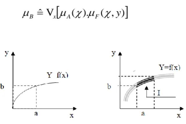
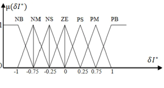
3.2. FUZZY LOGIC BASED CONTROL. ... 37
3.3. FUZZY LOGIC REVIEW. ... 38
3.3.1. Fuzzy Set. ... 38
3.3.2. Fuzzy Set Operation. ... 39
3.3.3. Linguistic Variable. ... 40
3.3.4. Fuzzy System. ... 40
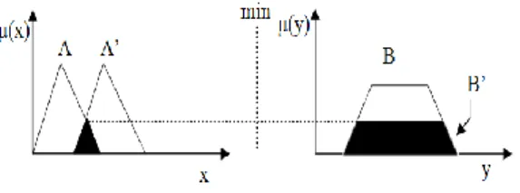
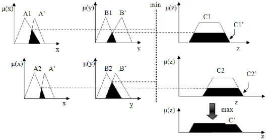
3.3.5. Fuzzy Rule. ... 42
3.3.6. Fuzzy Inference Process. ... 43
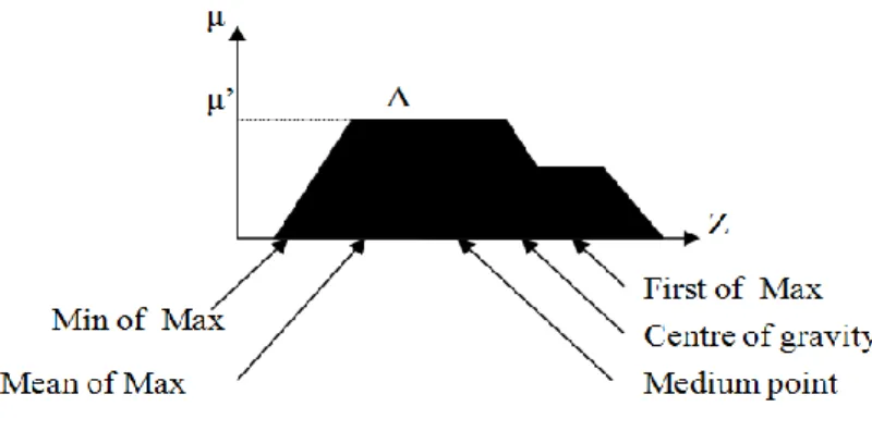
3.3.7. FLC step-by-step Design Procedure. ... 48
3.3.8. Implementation of the FLC. ... 49
3.4. REVIEW OF THE TESTED APPLICATIONS OF THE FLC AT POWER CONVERTERS ... 53
3.5. FUZZY LOGIC CONTROLLER FOR BOOST RECTIFIER ... 56
3.5.1. Fuzzyfication. ... 57 3.5.2. Decision-Making. ... 57 3.5.3. Defuzzyfication. ... 58 3.6. SIMULATION RESULTS. ... 60 3.7. CONCLUSION. ... 64 REFERENCES. CONCLUSION. ... 65
This study presents the analysis, a modeling approach to obtain a small-signal model, design and the Matlab/Similink implementation of a linear control technique for single-phase boost power factor correctors (PFC). Such converters present nonlinear characteristics and an approximation of them are used to drive the models. The most important result obtained is that the small-signal output is not equal to the load impedance. The proposed circuit significantly improves the dynamic response of the converter to load steps without the need of a high crossover frequency of the voltage loop by adding low-pass filter, so that a low distortion of the input current is easily achieved in PI-PI Control for Active Power Factor Correction. After that, a modeling approach to obtain a small-signal model and the simulation of a PI controller in the loop voltage and two controllers in the loop current based on a standard fixed and sinusoidal band hysteresis control, followed by a variable band hysteresis control for a single-phase power factor corrector (PFC). Finally, a fuzzy logic controller in the loop voltage and hysteresis controller in the loop current for a single-phase power factor corrector (PFC).
Key words: Power Factor, Rectifier, AC-DC, Correction, PI, Hysteresis, Fuzzy
RESUME.
Cette étude présente l'analyse, une approche de modélisation pour obtenir un modèle de signal unique, la conception et l'implémentation sous Matlab/Similink d'une technique de contrôle linéaire pour les correcteurs du facteur du puissance monophasés (PFC). Tels convertisseurs présentent des caractéristiques nonlinéaires et une approximation d'eux sont utilisées pour conduire les modèles. Le résultat le plus important obtenu est que la production d'un signal de sortie unique n'est pas égale à l’impédance de la charge. Le circuit proposé améliore considérablement la réponse dynamique du convertisseur pour les pas de la charge sans le besoin d'une haute fréquence de la boucle de tension en ajoutant un filtre passe - bas, afin qu'une basse distorsion du courant d'entrée soit atteindre facilement dans la commande PI-PI Pour la correction du facteur de puissance. Après cela, une approche de modélisation aussi pour obtenir un modèle de signal unique et la simulation d'un contrôleur PI dans la boucle de tension et deux contrôleurs dans la boucle du courant basé sur la commande hystérésis à bande fixe et à bande sinusoïdale, suivi par la commande hystérésis à bande variable et finalement, un contrôleur de la logique flou dans la boucle de tension et un contrôleur hystérésis dans la boucle du courant pour la correction du facteur de puissance
(PFC) en monophasé.
Mots clés : Facteur de puissance, redresseurs, AC-DC, Correction, PI, Hystérésis, floue
صخـــلم
.
،لاٍهحح اُن جيذق تساسذنا ِزه حهَو تخزًُنا زٍفُحو ىًٍصحو ةساشإ شٍغص جرىًَ ىهع لىصحهن بهطي حياَشب / كُهًٍٍس ل تٍطخنا ىكحخنا تٍُقح سىطنا تٌداحأ تعاطخسلاا مياع ثاححصًن . اهباسح و تٍطخ شٍغ ثافص وذقح ثلاىحًنا ِزه مثي تٍَوشخكنلاا جراًُنا ةداٍقن مًعخسٌ . ةذٍحو جوشخ ةساشإ جاخَإ ٌأ اهٍهع مصحخًنا تًهًنا تدٍخُنا تنىًحنا تعَاًي يواسح لا . شحىخنا تقهحن ًناع ددشح ىنإ تخاحنا ٌوذب تنىًحنا ثاىطخ مخَ لىحًهن تٍكٍياٌُذنا تبادخسلاا ةشثكب ٍسحح تحشخقًنا ةساذنا ىكحخنا ًف تنىهسب لىخذنا ساٍخن ضفخُي فاشحَا ىنإ مصىخهن ضفخُي سىبع ةافصي تفاضئب PI-PI مياع حٍحصخن تعاطخسلاا . بقاشي عٍُصح و ةساشلإا ذٍحو جرىًَ ىهع لىصحهن بٍكشخنا ، كنر ذعب PI ًف ٍٍبقاشي و شحىخنا تقهح ًف طٌشش ور ًعخاشخنا ىكحخناب عبخٌ ، ًبٍخ ًخىًح طٌشش ور شخآو جباث طٌشش ور ًعخاشخنا ىكحخنا ىهع سسؤي ساٍخنا تقهح قطًُنا بقاشي لاًعخسا ، اشٍخأ ، شٍغخي ًبابضنا مياعي حٍهصخن ساٍخنا تقهح ًف ًعخاشخنا بقاشًناو شحىخنا تقهح ًف تعاطخسلاا (PFC) سىطنا يداحأ واظُنا ًف . تيحاتفملا ثاملكلا : حٍحصح , PFC, PI, ثلاىحًنا AC/DC1
INTRODUCTION.
Most electronic equipment is supplied by 50 Hz utility power, and more than 50% of this power is processed through some kind of power converter. Usually power converters use a diode rectifier followed by a bulk capacitor to convert AC voltage to DC voltage. Since these power converters absorb energy from the AC line only when the line voltage is higher than the DC bus voltage, the input line current contains rich harmonics, which pollute the power system and interfere with other electric equipment. These converters usually have a low power factor.
When a converter has less than unity power factor, it means that the converter absorbs apparent power higher than the real power it consumes. This implies that the power source should be rated with higher VA ratings than the load needs. In addition, the current harmonics the converter produces deteriorate the power source quality, which eventually affect the other equipment. The simple solution to improve the power factor is to add a PFC to achieve a good power factor. called a PFC stage, is usually inserted in the equipment to shape the line input current into a sinusoidal waveform and its line current is in phase with the line voltage.
Among three basic power converter topologies (boost, buck and buck-boost), the boost converter is shown is the one most suitable for power factor correction applications. This is because the inductor is in series with the line input terminal through the diode rectifier, which gives lower line current ripple and continuous input current, the buck converter is seldom used as a power factor correction application, since the input current is discontinuous and it loses control when the line input voltage is lower than the output voltage. The buck-boost and flyback converters are able to control the average line input current. However, the power handling capability is smaller because of its higher voltage and current stresses. Therefore, the boost converter is currently the most popular PFC topology. To achieve unity power factor, the input power is the squared sine waveform while the output power is usually constant for most applications [1].
To meet the IEC requirements, a PFC circuit should be added in the system. A frequently used boost PFC circuit can be inserted into the system. However, after adding the PFC function, the cost of the system will increase and the efficiency of the system will decrease. [2]; a big number of the power factor correctors of AC/DC converters has been proposed in the literature, some practical works of simulation under Simulink (simulator of dynamic
2 systems under Matlab), will permit to validate the study, to examine rapidly different command modes of this converter, to observe unique or with difficulty measurable signals, Commonly, a linear controller (PI-PI controller) is designed utilizing a small-signal model that is obtained by linearization about an operating point [3] in both, outer loop for output dc voltage regulation (loop voltage) and inner loop so that the line current is sinusoidal and in phase with the line voltage (loop current). The system provides acceptable performance. In [4], a PI control scheme is presented that includes a 100 Hz notch filter in the voltage control loop. The notch filter reduces the amount of second harmonic that is reaching the multiplier. Thus, the voltage loop bandwidth can be increased, which leads to a faster transient response, without the penalty of increased third harmonic in line current in steady state. The improvement in the transient response of the loop voltage controller degrades the quality of the input current (High THD). On the other hand, PI controller design in loop current requires an accurate mathematical model of the plant and it failed to perform satisfactorily under parameter variation, nonlinearity (two multiplications), load disturbance, etc [5]. Hysteresis current controller (bang-bang hysteresis (BBH) technique) has an advantage in coping with the time varying nonlinearity of switches in PFC pre-regulator, and it does not require an accurate mathematical model of the PFC pre-regulator when the controller is being designed [6]. Also this technique has an advantage of yielding instantaneous current control [7], which results in very fast response and increased ‗boost‘ switch reliability. However, it has a serious disadvantage in that the switching frequency of the boost switch fsw is not constant and varies
in a wide range during each half cycle of the ac input voltage[8], [9]. The switching frequency is also sensitive to circuit component values, design parameters and difficult for EMI filter design. The novel feature of the proposed method resides in the fact that unity power factor and nearly sinusoidal inputs current are obtained at constant switching frequencies [10], [11]. Moreover, the method exhibits instantaneous current control, which results in very fast response and increased switch reliability.
The fuzzy approach also, offers the possibility to model a non–linear system on the basis of the knowledge of many non-well defined relations among the variables of the system, and to design a controller that adapts itself to several working conditions.
Thus, fuzzy logic seems a suitable solution both to model and to control power electronic systems [12].
PI-PI Control for Active Power Factor Correction in chapter 1 presents a systematic analysis, a modeling approach to obtain a small-signal model, design and digital implementation of the
3 standard cascaded linear controller along with using a 100 Hz notch filter in a voltage loop of a regulated dc voltage. This controller is verified by detailed MATLAB/Simulink based simulations through the use of a continuous time plant model and a discrete time controller. Chapter 2 covers a systematic design, and simulation comparison, PI controller for a voltage loop of a regulated dc voltage, standard hysteresis controller and redesign of the standard hysteresis controller with some modifications for improved performance for a current loop. All these controllers are verified by detailed MATLAB/Simulink based simulations using a continuous time plant model and a discrete time controller. These controllers are compared for steady-state performance and transient response over the entire range of input and load conditions for which the system is designed.
In Chapter 3; Fuzzy Logic Control for Active Power Factor Correction is proposed; in this case, PI controller will be replaced by fuzzy logic controller for a voltage loop of a regulated dc voltage; and standard hysteresis controller for a current loop. These controllers are verified by detailed MATLAB/Simulink based simulations using a continuous time plant model and a discrete time controller and are compared for steady-state performance and transient response.
REFERENCES.
[1]. Jinrong Qian. “Advanced Single-Stage Power Factor Correction Techniques”. Dissertation submitted to the faulty of the Virginia Polytechnic Institute and State University in partial fulfillment of the requirements for the degree of Doctor of Philosophy in Electrical Engineering. September 25, 1997
[2]. Yiqing Zhao. ―Single Phase Power Factor Correction Circuit with Wide Output Voltage Range”. Thesis submitted to the Faculty of the Virginia Polytechnic Institute and State University in partial fulfillment of the requirements for the degree of Master of Science In Electrical Engineering. February 6, 1998
[3]. Zaohong Yang and Paresh C. Sen. “A Novel Technique to Achieve Unity Power Factor and Fact Transient Response In Ac-to-Dc Converters,‖ IEEE Transaction on Power Electronics, vol. 16, no. 6, pp. 764–78, Novembre 2001.
[4]. L.Rahmani, F.Krim, A.Bouafia. “Deadbeat Control for PWM AC Chopper,‖ Taylor & Francis, Electric Power Components and systems, 32:453-466, 2004. [5]. L.Rahmani, F.Krim, M.S.Khanniche, A.Bouafia. ―Control for PWM AC Chopper
feeding nonlinear loads,” Taylor & Francis, INT. J. ELECTRONICS, Vol 91, No 3, March 2004, 149-163.
[6]. Diego G. Lamar, Arturo Fernandez, Manuel Arias. ―A Unity Power Factor Correction Preregulator With Fast Dynamic Response Based on a Low-Cost Microcontroller,” IEEE Transaction on Power Electronics, vol. 23, no. 2, pp. 635– 641, March 2008.
[7]. Martin K. H. Cheung, Martin H. L. Chow, Chi K. Tse. “Practical Design And Evaluation of A 1 KW PFC Power Supply Based en Reduced Redundant Power Processing Principle,‖ IEEE Transaction on Industrial Electronics, vol. 55, no. 2, pp. 665–673, February 2008.
[8]. Vishnu Murahari Rao, Amit Kumar Jain, Kishore K. Reddy and Aman Behal. “Experimental Comparison of Digital Implementation of Single-Phase PFC Controllers,‖ IEEE Transaction on Industrial Electronics, vol. 55, no. 1, pp. 67–78, January 2008.
[9]. John Chi Wo Lam and Praveen K Jain. ―A Modified Valley Fill Electronic Ballast Having a Current Source Resonant Inverter With Improved Line- Current Total Harmonic Distortion (THD), High Power Factor, and Low Lamp Crest Factor,‖ IEEE Transaction on Industrial Electronics, vol. 55, no. 3, pp. 1147–1159, March 2008.
[10]. N. Belhouchet and L.Rahmani. “Development of Adaptative Hysteresis-band Current Control of PWM Three-Phase AC Chopper with Constant Switching Frequency,‖ Taylor & Francis, Electric Power Components and systems, 37:583-598, 2009.
[11]. N. Belhouchet, L.Rahmani and S. Begag. “A novel adaptative HBCC technique for three-phase shunt APF,‖ Elsevier, Electric Power Systems Research, 79, 2009, 1097-1104.
[12]. Simon Wall and Robin Jackson. “Fast Controller Design for Single-Phase Power-Factor Correction Systems,‖ IEEE Transaction on Industrial Electronics, vol. 44, no. 5, pp. 654–660, October 1997.
CHAPTER 1
PI-PI CONTROL FOR ACTIVE POWER
4 Abstract—this chapter presents the analysis, a modeling approach to obtain a small-signal model, design and the Mathlab/Similink implementation of a linear control technique for single-phase boost power factor correctors (PFC). Such converters present nonlinear characteristics and an approximation of them are used to drive the models. The most important result obtained is that the small-signal output is not equal to the load impedance. The proposed circuit significantly improves the dynamic response of the converter to load steps without the need of a high crossover frequency of the voltage loop by adding low-pass filter, so that a low distortion of the input current is easily achieved. This controller has been verified via simulation in Simulink using a continuous time plant model and a discrete time controller.
1.1. INTRODUCTION.
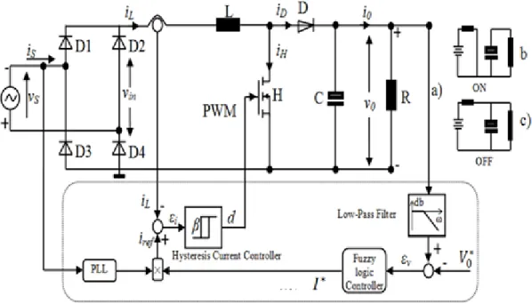
Single-phase power factor correction (PFC) circuits provide rectification of the line voltage to a regulated dc voltage while shaping the input current to be a sinusoid and in phase with the line voltage [1]. Often, the PFC acts as a preregulator to a dc–dc converter that may be used to provide additional regulation and ohmic isolation [2], [3]. Due to adoption of IEC 1000-3-2 [4] as the EN61000-3-2 norm in Europe and the formulation of the IEEE 519 [5] in the USA, these circuits are increasingly being used in the front-end of electronic equipment. Among the several possible topologies [2], the boost PFC shown in Fig. 1.3 is most commonly used. The control objectives are to track the inductor current to a rectified Sinusoid (so that the line current is sinusoidal and in phase with the line voltage) and to regulate the average output voltage to a desired magnitude and to has a fast response to the load variation [6], [7].
Commonly, a linear controller is designed utilizing a small-signal model that is obtained by linearization about an operating point [6]. The system provides acceptable performance. However, the controller has an inherent drawback of third harmonic in the input current. This happens because the reference current signal is the product of an output voltage error amplifier (that contains a second-harmonic component) and the input voltage wave shape. Thus, the voltage loop gain at 100 Hz effectively determines the level of third harmonic to be expected in the input voltage [8]. Several commercial ICs incorporate the required analog components to implement the linear control scheme. Recently, there has been a significant interest in an all-digital implementation, available
5 for the PFC application, digital implementation of the linear control design using commercial microcontrollers and DSPs has been carried out. Since the computation time of commercial low-cost microcontroller is significantly high, a discrete version of the conventional analog design cannot be directly implemented without significant modification to the design of the voltage control loop. To improve the dynamic response of the converter to load steps, the 100 Hz notch filter is inserted to the voltage control loop. The notch filter reduces the amount of second harmonic (to cancel the output voltage ripple) that is reaching the multiplier. Thus, the voltage loop bandwidth can be increased, which leads to a faster transient response, without the penalty of increased third harmonic in steady state. For faster dynamic response, current mode control is adopted instead of voltage mode control. Both peak current mode and average current mode controls are widely used [9]. The main deference between the two methods is that, in the later, the sensed inductor current signal is averaged and compensated by a current compensation network [10], while in the former; only inductor current is sensed and used [11]-[12]. Although noise in average current mode control can be suppressed, the architecture of the system with average current mode control is complicated. Therefore, peak current mode control is used, and an optimal proportional integral (PI) controller designed by utilizing a small-signal model is adopted to achieve fast dynamic response, simplicity, and easy implementation. This chapter presents a systematic analysis, a modeling approach to obtain a small-signal model, design and digital implementation of the standard cascaded linear controller along with using a 100 Hz notch filter in a voltage loop of a regulated dc voltage. This controller is verified by detailed MATLAB/Simulink based simulations through the use of a continuous time plant model and a discrete time controller.
1.2. CLASSIC CONVERTER.
Fig. 1.1 represents the solution commonly adopted for the conversion in single phase AC-DC. It is about a full bridge of four diodes rectifier feeding a RC load.
Fig. 1.2 represents the simulation waveforms of DC-Bus voltage, of the input current and its spectrum. The input current is much distorted due to large discontinuities with THD of 69.77%
6 Fig. 1.1. Full Bridge Rectifier.
Fig.1.2. The input current and DC-Bus Voltage R=212 Ω, C=940 μF, L= 37.3 mH, VSM=150 V.
As we observe in Fig. 1.2 the deformation in the shape of the input current, therefore, the power factor at the input side is variable and weak in some cases because of the raised harmonic distortion of the current wave.
To limit the ominous effects of the LF disruptions, the norm IEC 61000-3-2 governs, the harmonic of the current absorbed by the network for currents not exceeding 16A by phase is about 3,7 KVA in single phase. Therefore, it is necessary to put to the point of the solutions permitting to reduce the LF disruptions of AC-DC classic converter. These solutions, regrouped under the name (Power Factor Correction or PFC), must permit to
7 absorb on the network a current the more sinusoidal possible with a minimum of phase angle between the fundamental of the current absorbed and the input voltage.
Fig.1.3. PFC preregulator.
Fig.1.4. Block diagram of the PFC preregulator. 1.3. PRINCIPALS OF OPERATION.
The basic circuit diagram of the dc/dc converter with front–end solid-state input power factor conditioner used in the proposed scheme is shown in Fig.1.3a and Fig.1.4.
The power circuit is that of an elementary step-up converter. When the boost switch H is turned on (d=1) Fig.1.3b, the inductor current builds up, and energy is stored in the
8 magnetic field of the inductor, whereas the boost diode D is reverse biased, and the capacitor supplies power to the load. This is the first mode operation. As soon as the boost switch is turned off (d=0) Fig.1.3c, the power circuit changes mode, and the stored energy in the inductor, together with the energy coming from the input ac source, is pumped to the output circuitry (capacitor-load combination). This is mode 2 of the circuit. Then the state space model for the boost PFCS in continuous current mode can be found by the circuit analysis of fig.1a. The output voltage and inductor current dynamics are governed by the variable structure real switched system equations (1.1).
𝑑𝑣0 𝑑𝑡 = 1 𝐶 1 − 𝑑 𝑖𝐿− (1/𝑅)𝑣0 𝑑𝑖𝐿 𝑑𝑡 = 1 𝐿 𝑣𝑖𝑛 − (1 − 𝑑)𝑣0 (1.1)
In order to obtain a sinusoidal input current in phase with the input voltage, the control unit should act in such a way that vin sees a resistive load equal to the ratio of vin and iL.
This has been done by comparing the actual current passing through the inductor with a current reference, which is derived from vin and has amplitude determined by the output
voltage controller.
Since the break frequency of the output filter is very low, one can say that the output voltage is controlled only by the average value of the on-duty ratio of the switch in half cycle of the ac input voltage α:
𝑉0 =𝑉𝑖𝑛 ,𝑎𝑣𝑒 1 − 𝛼 = 2 𝜋𝑉𝑆𝑀 1 1 − 𝛼 (1.2) Where
d : Logical variable to represent the state of the boost switch,
Vin,ave : average value of the full-wave rectified sinusoidal input voltage,
9 1.4. STATIC ANALYSIS OF POWER FACTOR CORRECTOR PREREGULATORS
WITH FAST DYNAMICS.
The control by current imposes the average power
𝑃 = 1 𝑇/2 𝑣𝑆(𝑡) 𝑖0 𝑡 𝑑𝑡 𝑇/2 0 = 1 𝑇/2 𝑉𝑆𝑀𝑠𝑖𝑛𝜔𝑡 𝑇/2 0 𝐼𝑟𝑒𝑓𝐷𝐶𝑠𝑖𝑛𝜔𝑡 𝑑𝑡 =𝑉𝑆𝑀𝐼𝑟𝑒𝑓𝐷𝐶 2 (1.3)
passed to the load with the ideal PFC preregulators. This behavior in generator of power lets free the voltage vS to progress according the load R in the report vS2/R. Generally, the
users ask for generators of voltage. It follows the necessity of an automatic adaptation of the power supplied to the load according to its variations to maintain 𝑣𝑠. Fig.1.3a shows
the voltage loop 𝑣𝑠 of which the gating control signal will act on the amplitude of the reference current with a constraint of sinusoidal shape.
A low-pass filter is included in the output voltage feedback loop to eliminate 100 Hz output voltage ripple Fig.1.5. The output of the voltage feedback loop is therefore a DC value IrefDC. The input line current reference is therefore a sinusoidal waveform and the
input line current iS(t) (assuming the current loop to be ideal) has no distortion.
𝑖𝑆(𝑡) =
𝑉𝑆𝑀 sin(𝜔𝑡) 𝐼𝑟𝑒𝑓𝐷𝐶
𝐾𝑠 (1.4)
PFC preregulators have a high efficiency (around 95%). So
𝑣𝑆(𝑡)𝑖𝑆(𝑡) = 𝑉0𝐷𝐶𝑖0(𝑡) (1.5)
Moreover, the output capacitor C is big enough to keep the output voltage to his DC component V0DC. So 𝑖0(𝑡) = 𝑉𝑆𝑀2 𝐼 𝑟𝑒𝑓𝐷𝐶 2𝐾𝑠𝑉0𝐷𝐶 1 − cos(2𝜔𝑡) (1.6)
10 Fig. 1.5. Voltage Loop.
As can be seen in Fig.1.5 and in (1.6), the output current has a DC Value and a second harmonic. This second harmonic is processed through the bulk capacitor. A voltage ripple thus appears at the output voltage and is transmitted into the output voltage feedback loop. For this reason, a low-pass filter is needed in order to attenuate and quasi- eliminate this distortion and keep the input line current sinusoidal, as can be seen in (1.4). However, the low-pass filter decreases the feedback bandwidth of the output voltage, causing a poor dynamic response of the output voltage in PFC preregulators. This chapter will next consider the situation in which the corner frequency of the low-pass filter (fCV)
place in the output voltage feedback is increased in order to improve the response of the output voltage in PFC preregulators. The PFC preregulator‘s priorities change: the main objective is to improve the output response instead of drawing a sinusoidal input current to obtain PFC preregulators with fast dynamics. The output voltage ripple of double line frequency is transferred into the output voltage feedback loop. Thus, the output of the voltage feedback loop (iref is not a constant value).
𝑖𝑟𝑒𝑓 𝑡 = 𝐼𝑟𝑒𝑓𝐷𝐶 + 𝐼𝑟𝑒𝑓𝐴𝐶sin(2𝜔𝑡 − ∅) (1.7)
Where IrefAC is the second harmonic amplitude of iref and Ø is the phase lag with respect
to |vs(t)| of the second harmonic of iref.
From Fig.1.5 and by replacing the value of IrefDC for iref(t) in (1.4)
𝑖𝑆(𝑡) = 𝑉𝑆𝑀 𝐾𝑠 𝐼𝑟𝑒𝑓𝐷𝐶 sin 𝜔𝑡 + 𝐼𝑟𝑒𝑓𝐴𝐶 2 cos 𝜔𝑡 − ∅ − 𝐼𝑟𝑒𝑓𝐴𝐶 2 cos 3𝜔𝑡 − ∅ (1.8)
The input current, therefore, is not sinusoidal. The second harmonic of iref(t) is
transformed into the third harmonic of the input line current. Furthermore, input line current distortion is defined by the ripple characteristics of the output of the voltage
11 feedback loop (IrefAC and Ø)
Substituting (1.8) in (1.5) and supposing an output bulk capacitor big enough to keep the output voltage constant, the output current is
𝑖0 𝑡 = 𝐼0+ 𝑖02 𝑡 + 𝑖04 𝑡 (1.9)
Moreover, KS can be easily calculated as a function of averaged power processed by the
PFC preregulator from I0 in (1.9)
The average power processed to the load become
𝑃 = 𝑉𝑆𝑀2 2𝐾𝑠(𝐼𝑟𝑒𝑓𝐷𝐶 + 𝐼𝑟𝑒𝑓𝐴𝐶 2 𝑠𝑖𝑛∅) (1.10) Then 𝐾𝑠 = 𝑉𝑆𝑀2 2𝑃 (𝐼𝑟𝑒𝑓𝐷𝐶 + 𝐼𝑟𝑒𝑓𝐴𝐶 2 𝑠𝑖𝑛∅) (1.11)
If the ripple of the output feedback loop IrefAC and the phase leg Ø are assumed to be
equal 0 and replacing P obtained from (1.3) in (1.11), the expressions of P and KS
become: P=(VSM IrefDC)/2, KS=VSM
1.5. DESIGN EXAMPLE.
Table 1.1
The power circuit is designed to meet the following specification: Output power
Output voltage Output voltage ripple Input voltage
Input current ripple Switching frequency Load resistance P0=132W V0=160V <2% VSeff=110V, RMS ≤5% fsw=20kHz R=212Ω Input Inductance L=22.5mH Output Capacity C=940µF
12
A. Design of L
The inductor current is controlled by two voltages; one is the rectified sinusoidal input voltage, which is applied to one side of the inductor, and the other one is the voltage across the switch, which varies between zero and v0 due to switching and is applied to the
other side of the inductor. The voltage that contributes to the ripple is the voltage across the switch. In other words, it can be said that the ripple current is produced by an equivalent wave of amplitude V0/2 and frequency equal to the switching frequency. To
consider the worst case for ripple, the duty cycle of the switch is taken to be 50% for this analysis. Based on the above assumptions, output voltage 𝑣0, switching frequency fsw,
inductance value L, and RMS value of the fundamental component of current ripple at 50% duty cycle I1r are related through the following:
𝑉0
2 4
𝜋 2 = 2𝜋𝑓𝑠𝑤𝐿 𝐼1𝑟 (1.12)
Note that 𝑉20 4
𝜋 2 is the RMS value of the fundamental component of the switched
voltage for a 50% duty cycle. In addition, the fundamental or switching frequency component of the current ripple represents more than 99% of the total RMS current generated by the square-wave voltage ripple.
The maximum permitted amount of ripple is 5%; therefore, I1r=0.05IL (Where IL is the
RMS value of the100Hz component of the inductor current).Therefore.
𝐿 = 1 2𝜋20.05 𝑉0 𝑓𝑠𝑤𝐼𝐿 = (1.437) 𝑉0 𝑓𝑠𝑤𝐼𝐿 (1.13)
With the values chosen before, L is found to be 6.59mH.
From (1.13) it is very clear that to reduce L to the small values we must increase the switching frequency fsw, the boost-type PFC converter tends to decrease the volumetric
13
B. Design of C
To find the value of C for a desired output voltage ripple, we note that the capacitor-resistor combination at the output of the converter acts as low-pass filter for the current through the boost diode. Considering, only its dc and fundamental components. Therefore
𝑖0(𝑡) ≅ 𝑘0(1 − 𝑐𝑜𝑠2𝜔𝑡) (1.14)
By comparing (1.5) and (1.14) and with the ideal voltage loop (KS=VSM) k0 is
𝐾0 = 𝑉𝑆𝑀2 𝐼 𝑟𝑒𝑓𝐷𝐶 2𝐾𝑠𝑉0𝐷𝐶 = 𝑉𝑆𝑀𝐼𝑟𝑒𝑓𝐷𝐶 2𝑉0𝐷𝐶 (1.15)
The gain of the filter for the dc component of the current i0 is R and for the ac component
is: 𝐺𝑎𝑐 = 𝑅 ((2𝑅𝐶𝜔)2+ 1)1 2 (1.16) Therefore 𝜏𝑜𝑛𝑑 = 2 𝐺𝑎𝑐 𝐺𝑑𝑐 = 2 ((2𝑅𝐶𝜔)2+ 1)1 2 (1.17) Then 𝐶 =(4 − 𝜏𝑜𝑛𝑑2) 1 2 2𝜏𝑜𝑛𝑑𝑅𝜔 (1.18)
14 1.6. VOLTAGE-LOOP CONTROLLER.
The components of the DC-DC converter are being considered ideal. Under this assumption, the total instantaneous power will be independent from the instantaneous power of the converter. And assuming that 𝑖𝐿 ≅ 𝑖𝑟𝑒𝑓
Where 𝑃 1 − 𝑐𝑜𝑠2𝜔𝑡 = 𝑣0𝑖𝐷 = 𝑣0 𝐶 𝑑𝑣0 𝑑𝑡 + 𝑣0 𝑅 (1.19)
It is certain that the output voltage ripple at 100 Hz is not interesting at all the calculation of the voltage controller whose bandwidth will be very weak (some hertz), to satisfy the constraint shape of the current iL.
We can so, considering that the equation (1.19) established for the instantaneous power can be reduced to that of the average power. The essential difference will concern the disappearance of the ripple at100 Hz of this voltage, ripple due to the fluctuating power. The action of the controller will be to maintain the mean value of the output voltage and not the instantaneous value, (1.19) Becomes:
𝑉𝑆𝑀𝐼𝑟𝑒𝑓𝐷𝐶 2 ≅ 𝐶 𝑑𝑉0𝐷𝐶2 𝑑𝑡 + 𝑉0𝐷𝐶2 𝑅 (1.20)
The indication DC is used to remind that only the mean value of v0 is expressed in this
equation. As can be seen in (1.20), the regulation of V0DC is made possible by action on
the amplitude of IrefM fig.1.6. To calculate the controller parameters the above equation is
nonlinear and is therefore linearized around the operating point defined by (V0DCC and
IrefDCC)
The transfer function of the system TV(s) is obtained:
𝑇𝑉 𝑠 = 𝛿𝑉0𝐷𝐶 𝛿𝐼𝑟𝑒𝑓𝐷𝐶 = 𝑉𝑆𝑀 4𝑉0𝐷𝐶𝐶 𝑅 1 + 𝑅𝐶𝑠 (1.21)
The voltage loop controller CV(s) is usually a first order lag given by the following
15 𝑘𝑃𝐼 = 𝑅𝐶 𝑇𝑃𝐼, 𝑇𝑃𝐼 = 𝐵𝑅𝑉𝑆𝑀 8𝜋(𝑓𝐶𝑉)𝑉0𝐷𝐶𝐶 (1.22) Where
B: the attenuation of the measured output voltage, fCV : voltage closed loop crossover frequency.
Fig.1.6 Voltage loop controller.
Pole and gain are chosen to obtain a sufficient phase margin gain (≈45°) and bandwidth in the 5 to 20 Hz range. The bandwidth is intentionally kept very low since the compensator gain at 100 Hz effectively determines the third harmonic to be expected in the input current. Since the outer loop has a finite dc gain, the voltage reference is pre-compensated to avoid a steady state voltage error at nominal operation.
1.7. CURRENT-LOOP CONTROLLER.
The boost PFCS of Fig.1.3 is nonreversible, so to avoid crossover distortion, it is essential that the phase difference between iL and vin is negligible. In cascade control
structure, this requirement is satisfied if the current loop has excellent tracking. The full-wave rectified signal vin has no significant harmonic content above 1 kHz. Therefore,
adequate tracking should be possible with a current loop crossover frequency, fCI =5-10
kHz. However, due to the nonlinear nature of (1.1), a linear controller cannot be used
without iL becoming distorted [10]. The distortion can be avoided if, in the closed loop,
the state-space averaged input current dynamics are linear in the large. This can be achieved through the use of suitable nonlinear controller designed using formal feedback linearization methods [11]. In this case, the correct controller form for feedback linearization can be found by inspection:
16 Assuming that the output voltage is constant V0, then equation (1.1) becomes
1 − 𝑑 = 1 𝑉0
2
𝜋𝑉𝑆𝑀− 𝐶𝐼(𝑠) 𝑖𝑟𝑒𝑓 − 𝑖𝐿 (1.23)
Fig.1.7. Current loop controller.
A block diagram of the controller is depicted in Fig 1.7. The state-space averaged open loop transfer function of the current loop is CI(s)TI(s), Where the plant transfer function
TI(s) is defined by.
𝑇𝐼(𝑠) = 1
𝑠𝐿 (1.24)
The compensator CI(s) is designed to obtain an acceptable phase margin and a bandwidth
of the order of 10 KHz
1.8. SIMULATION RESULTS.
A comprehensive simulation and real-time experimental study were performed to capture the performance of the proposed PI_PI control for single-phase power factor correction. First, the steady-state performance is evaluated in terms of output voltage regulation, THD, and power factor. Next, the transient performance is evaluated for output voltage response on application of load step changes that are expected in practical applications of this circuit.
1) steady-state performance: Fig.1.8 illustrates the simulated waveforms, dc-bus voltage,
17 easy viewing) in the steady-state with a unity power factor, for the PI_PI control at nominal load and nominal line voltage—these waveforms have been appropriately shifted in time to be visible. From this figure, it can be seen that the results obtained with the proposed PI_PI control are much better than the adoption of IEC 1000-3-2 [4] as the EN61000-3-2 norm in Europe and the formulation of the IEEE 519 [5] in the USA. Line current is very close to sine wave and in phase with the power source voltage—the THD is 2.97%. It is important to note that at nominal line and load condition, the PI_PI control has THD number below 3% even with the limited bandwidth that is allowed by the digital implementation. As far as steady-state error in the output voltage is concerned— the steady-state error is 1V.
2) Transient performance: As previously stated, step load changes are effected by connecting (or disconnecting) parallel load. The reference current amplitude is limited to
3.5A in the control for the PI_PI control designs.
Fig.1.9 shows the transient response for the proposed PI_PI control for single-phase power factor correction for a load resistor step from 212Ω to 312 Ω and from 312Ω to
212 Ω. After a short transient, the dc-bus voltage is maintained close to its reference
value with a good approximation and stability. The line currents have nearly sinusoidal waveforms. The corresponding transient values are shown in table 1.2.
The dynamic behavior of the proposed PI_PI under a step change of V*0 is presented in
Fig.1.10. After a short transient, the dc-bus voltage is maintained close to its new reference with good approximation and stability. The line currents have nearly sinusoidal waveforms. The corresponding transient values are shown in table 1.3.
Fig. 1.11 shows the transient of the step change of vs in the proposed PI_PI control by
decreasing vs from 150 V to 140 V and increasing them from 140 V to 150 V. After a short
transient, the dc-bus voltage is maintained close to its new reference with good approximation and stability. The line currents have nearly sinusoidal waveforms. The corresponding transient values are shown in table 1.4.
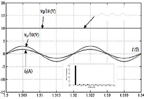
18 Fig.1.8 Simulated basic signal waveforms in steady state
under UPF, V*0=160 V, THD=2.97%.
Fig. 1.9 Transient of the step change of the load Increasing from 212Ω to 312Ω and Decreasing from 312 Ω to 212Ω.
19 Fig. 1.10 Transient of the step change of V*0, Increasing
from 160 V to 192 V and Decreasing from 192 V to 160 V.
Fig. 1.11 Transient of the step change of vs, decreasing
20 Table1. 2
Transient values corresponding to Fig. 1.9.
Load V0 (V) t (S) Iref (A) t (S)
212Ω/312Ω 12.8 0.7 0.52 0.5
312Ω/212Ω 12.8 0.7 0.52 0.5
Table 1.3
Transient values corresponding to Fig.1. 10.
V*0 V0 (V) t (S) Iref (A) t (S)
160V/192V 32 0.8 0.7 1
192V/160V 32 0.8 0.7 1
Table 1.4
Transient values corresponding to Fig.1. 11.
vs Vs (V) t (S) Iref (A) t (S)
150V/140V 3.2 0.7 0.14 0.8
140V/150V 3.2 0.7 0.14 0.8
1.9. CONCLUSION.
In this chapter, the simulation design constraints of power-factor-correction power supplies that use a cascading structure to achieve high power factor and fast regulation have been study. In addition, the small-signal model of the proposed converter was developed, from witch an optimal PI compensator is designed for the converter system with peak-current mode control. However, the input current harmonic content is very close to the limit. Simulations results have been shown that fast dynamic response; good output regulation, low harmonic distortion, and high power factor can be achieved with the proposed single-stage converter and control scheme.
REFERENCES.
[1] Yu Qin, Shanshan Du. ―Fuzzy logic and digital PI control of single phase power factor pre-regulator for an online UPS-a comparative study” Industrial Technology, 1996. (ICIT apos; 96), Proceedings of The IEEE International Conference on Volume, Issue, 2-6 Dec 1996 pp. 103 – 107.
[2] Ahmed H. Mitwali, Steven B. Leeb, George C. Verghese and V. Joseph Thottuvelil. “An Adaptive Digital Controller for a Unity Power Factor Converter,” IEEE Transaction on Power Electronics, vol. 11, no. 2, pp. 374–382, March 1996.
[3] Simon Wall and Robin Jackson. “Fast Controller Design for Single-Phase Power-Factor Correction Systems,” IEEE Transaction on Industrial Electronics, vol. 44, no. 5, pp. 654–660, October 1997.
[4] Tsai-Fu Wu and Yu-Kai Chen. “Analysis and Design of an Isolated Single-Stage Converter Achieving Power-Factor Correction and Fast Regulation,” IEEE Transaction on Industrial Electronics, vol. 46, no. 4, pp. 759–767, August 1999.
[5] Jee-Woo Lim and Bong-Hwan Kwon. “A Power-Factor Controller for Single Phase PWM Rectifier,” IEEE Transaction on Industrial Electronics, vol. 46, no. 5, pp. 1035– 1037, October 1999.
[6] Zaohong Yang and Paresh C. Sen. “A Novel Technique to Achieve Unity Power Factor and Fact Transient Response In Ac-to-Dc Converters,” IEEE Transaction on Power Electronics, vol. 16, no. 6, pp. 764–78, Novembre 2001.
[7] Fu M. Chen Q. “Applied Power Electronics Conference and Exposition”, 2001, APEC, 2001, Sixteenth Annual IEEEVolume 1, Issue, 2001 pp. 144 - 149 vol.1.
[8] Masashi Ochiai and Hirofumi Matsuo. “An AC/DC Converter with High Power Factor,‖ IEEE Transaction on Industrial Electronics, vol. 50, no. 2, pp. 356–361, April 2003.
[9] Diego G. Lamar, Arturo Fernandez, Manuel Arias. ―A Unity Power Factor Correction Preregulator With Fast Dynamic Response Based on a Low-Cost Microcontroller” IEEE Transaction on Power Electronics, vol. 23, no. 2, pp. 635–641, March 2008.
[10] Martin K. H. Cheung, Martin H. L. Chow, Chi K. Tse. “Practical Design And Evaluation of A 1 KW PFC Power Supply Based en Reduced Redundant Power Processing Principle,‖ IEEE Transaction on Industrial Electronics, vol. 55, no. 2, pp. 665–673, February 2008.
[11] Vishnu Murahari Rao, Amit Kumar Jain, Kishore K. Reddy and Aman Behal. “Experimental Comparison of Digital Implementation of Single-Phase PFC Controllers,‖ IEEE Transaction on Industrial Electronics, vol. 55, no. 1, pp. 67–78, January 2008.
[12] John Chi Wo Lam and Praveen K Jain. “A Modified Valley Fill Electronic Ballast Having a Current Source Resonant Inverter With Improved Line- Current Total Harmonic Distortion (THD), High Power Factor, and Low Lamp Crest Factor,‖ IEEE Transaction on Industrial Electronics, vol. 55, no. 3, pp. 1147–1159, March 2008.
CHAPTER 2
PI-HYSTERESIS CONTROL FOR ACTIVE
21
Abstract—this Chapter presents a modeling approach to obtain a small-signal model and the
simulation of a PI controller in the loop voltage and two controllers in the loop current based first on a standard fixed and sinusoidal band hysteresis control, followed by a variable band hysteresis control for a single-phase power factor corrector (PFC). All these controllers have been verified via simulation in Simulink using a continuous time plant model and a discrete time controller. All these controllers are compared for steady-state performance and transient response. It is shown that the PI controller gives a better steady-state performance under large load disturbance and plant uncertainties, whereas the variable band hysteresis control in the loop current gives a low THD of the input current compared to a standard classical fixed and sinusoidal band hysteresis control.
2.1. INTRODUCTION.
Single-phase power factor correction (PFC) circuits provide rectification of the line voltage to a regulated dc voltage while shaping the input current to be a sinusoid and in phase with the line voltage [1]. Often, the PFC acts as a preregulator to a dc–dc converter that may be used to provide additional regulation and ohmic isolation [2], [3]. Due to adoption of IEC 1000-3-2 [4] as the EN61000-3-2 norm in Europe and the formulation of the IEEE 519 [5] in the USA, these circuits are increasingly being used in the front-end of electronic equipment. Among the several possible topologies [2], the boost PFC shown in Fig. 2.1 is most commonly used. The control objectives are to track the inductor current to a rectified Sinusoid (so that the line current is sinusoidal and in phase with the line voltage) and to regulate the average output voltage to a desired magnitude and to has a fast response to the load variation [6], [7].
Commonly, a linear controller (PI-PI controller) is designed utilizing a small-signal model that is obtained by linearization about an operating point [6] in both, outer loop for output dc voltage regulation (loop voltage) and inner loop so that the line current is sinusoidal and in phase with the line voltage (loop current). The system provides acceptable performance. In [9], a PI control scheme is presented that includes a 100 Hz notch filter in the voltage control loop. The notch filter reduces the amount of second harmonic that is reaching the multiplier. Thus, the voltage loop bandwidth can be increased, which leads to a faster transient response, without the penalty of increased third harmonic in line current in steady state. The improvement in the transient response of the loop voltage controller degrades the quality of the input current (High THD). On the other hand, PI controller design in loop current requires an accurate mathematical model of the plant and it failed to perform satisfactorily under parameter
22 variation, nonlinearity (two multiplications), load disturbance, etc [10]. Hysteresis current controller (bang-bang hysteresis (BBH) technique) has an advantage in coping with the time varying nonlinearity of switches in PFC pre-regulator, and it does not require an accurate mathematical model of the PFC pre-regulator when the controller is being designed [11]. Also this technique has an advantage of yielding instantaneous current control [12], which results in very fast response and increased ‗boost‘ switch reliability. However, it has a serious disadvantage in that the switching frequency of the boost switch fsw is not constant and varies in
a wide range during each half cycle of the ac input voltage[13], [14]. The switching frequency is also sensitive to circuit component values, design parameters and difficult for EMI filter design. The novel feature of the proposed method resides in the fact that unity power factor and nearly sinusoidal inputs current are obtained at constant switching frequencies [15] [16]. Moreover, the method exhibits instantaneous current control, which results in very fast response and increased switch reliability.
This chapter presents a systematic design, and simulation comparison: 1) of a PI controller with a 100 Hz notch filter for a voltage loop of a regulated dc voltage, 2) standard hysteresis controller and redesign of the standard hysteresis controller with some modifications for improved performance for a current loop. All these controllers are verified by detailed MATLAB/Simulink based simulations through the use of a continuous time plant model and a discrete time controller. These controllers are compared for steady-state performance and transient response over the entire range of input and load conditions for which the system is designed. The chapter is organized as follows. In Section 2.1, we describe the system dynamics and lay down the control objectives. Sections 2.2 and 2.3 present the design and analysis for the outer and inner controllers. Section 2.4 and 2.5 presents the details of the simulations and results. Section 2.6 concludes with discussions of the results.
23 Fig.2.1. PFC preregulator.
2.2. VOLTAGE-LOOP CONTROLLER.
As shown in Fig.2.2, the dc-bus voltage v0 is sensed and compared with a reference value 𝑉0∗.
The obtained error is used as input for the PI controller, the output of the controller IrefM
multiplied by sinωt obtained from PLL stage with sensing of the input voltage is the instantaneous reference current command iref.
The system in Fig. 1.1is modeled as a first order system:
𝑣0 𝐼𝑟𝑒𝑓𝑀 = 𝑉𝑆𝑀 4𝑉0∗ 𝑅 1 +𝑅𝐶2 𝑝= 𝑘𝑠 1 + 𝜏𝑠𝑝 (2.1)
24 The transfer function of the PI controller is: 𝑇
𝑖𝑃
The PI parameters are chosen as: 𝐾𝑖 =2𝑇𝑅𝐶 𝑖, 𝑇𝑖 =
𝐴𝑅𝑉𝑆𝑀
8𝜋𝑓𝐶𝑉𝑉0∗
Where
fCV : voltage closed loop crossover frequency.
With fCV=10Hz, then Ki=2.0160 and Ti=0.0494.
Then the closed loop transfer function with the design example given in table 2.1 is:
𝑣0 𝑉0∗ == 𝑘𝐹 1 + 𝜏𝐹𝑝= 16 1 + 0, O159𝑝 (2.2)
The power circuit is designed to meet the following specification: Table 2.1
Design specification and circuit parameters. Switching frequency fsw=20kHz
Output power P0=121W
AC amplitude of supply voltage VSM=150V
DC output voltage V0=160V
Input current ripple ≤2.5%
Output voltage ripple ≤2%
Load resistance R=212Ω
Input Inductance L=22.5mH
25 Fig.2.3 show the Bode plot of the voltage controlled system.
Fig.2.3 Bode plot of the voltage controlled system
Pole and gain are chosen to obtain a sufficient phase margin gain (≈45°) and bandwidth in the 5 to 20 Hz range. The bandwidth is intentionally kept very low since the compensator gain at 100
Hz effectively determines the third harmonic to be expected in the input current. Since the outer
loop has a finite dc gain, the voltage reference is pre-compensated to avoid a steady state voltage error at nominal operation.
2.3. CURRENT-LOOP CONTROLLER.
The Single-phase power factor correction (PFC) circuit analyzed here has a feedback loop such that the switching mode is determined by comparison of the actual current and sinusoidal reference current supplied form voltage loop controller in both ways the actual current in the first oscillates in fixed band hysteresis (FBH), in the second way oscillates in sinusoidal band hysteresis (SBH) as shown in Fig.2.4. And in the third way the actual current oscillates in variable band hysteresis (VBH).
26 Fig.2.4 Switching frequency.
Fig.2.5 Current error and the switch H voltage.
A. CONVENTIONAL HYSTERESIS CURRENT CONTROL. 1. Fixed Band Control.
In this scheme, the hysteresis bands are fixed throughout the fundamental period. The algorithm for this scheme is given as:
Upper band (iupper) =IrefMsinωt+ΔI= IrefMsinωt+β/2
Lower band (ilower) =IrefMsinωt-ΔI=IrefMsinωt-β/2
Where β=2ΔI is band hysteresis. If iL> iupper, d=0 then, vH=V0
27 2. Sinusoidal Band Control .
In this scheme, the hysteresis bands are sinusoidal throughout the fundamental period. The algorithm for this scheme is given as:
Upper band (iupper) = (IrefM +ΔI) sinωt = (IrefM +β/2)sinωt
Lower band (ilower) = (IrefM -ΔI) sinωt= (IrefM -β/2) sinωt
Where β=2ΔI is band hysteresis. If iL> iupper, d=0 then, vH=V0
If iL< ilower, d=1 then, vH=0
3. Control characteristics.
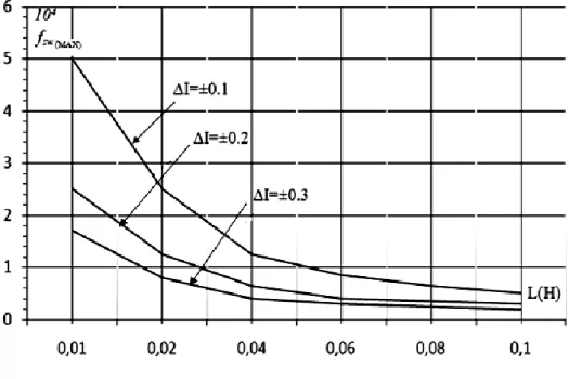
To investigate the control characteristics of a single-phase power factor corrector (PFC), the variation of maximal switching frequency with the inductance L of ΔI parameter for both techniques FBH and SBH is evaluated as seen in Fig.2.6. From Fig.2.4 and (2.5), by considering the output voltage V0 constant over a switching period we can write:
𝑡𝑜𝑛 = 𝐿
𝑣𝑖𝑛 𝐼𝑏− 𝐼𝑎 , 𝑡𝑜𝑓𝑓 = 𝐿
𝑣𝑖𝑛 − 𝑉0 𝐼𝑐 − 𝐼𝑏 (2.3)
Then the switching frequency is:
𝑓𝑠𝑤 = 1 𝑇𝑆𝑊 =
1
𝑡𝑜𝑛 + 𝑡𝑜𝑓𝑓 (2.4)
From Fig.2.1, the vH voltage is given by the following equation:
𝑣𝑖𝑛 − 𝐿𝑑𝑖𝐿
𝑑𝑡 = 𝑣𝐻 (2.5)
For the ideal PFC operation, we can assume the current iL to the reference rectifier
28 𝑣𝑖𝑛 − 𝐿𝑑𝑖𝑟𝑒𝑓
𝑑𝑡 = 𝑣𝐻∗ (2.6)
From (2.5) and (2.6), we obtained
𝐿𝑑𝜀𝑖
𝑑𝑡 = 𝑣𝐻 − 𝑣𝐻∗ (2.7)
Where:
εi=iref-iL: is the error current in the band of the hysteresis,
𝑣𝐻∗ : is the interrupter reference voltage corresponding to the ideal PFC operation.
From (2.7), if we assume the quantity 𝑣𝐻 − 𝑣𝐻∗ constant during the switching period, then the error current εi(t) varied as triangular form as shown in Fig.2.5
ton and toff obtained above in (3), can be find with another form using Fig.2.4 and equation
(2.7): 𝑡𝑜𝑛 = 𝐿𝛽 𝑣𝐻∗ , 𝑡𝑜𝑓𝑓 = 𝐿𝛽 𝑉0− 𝑣𝐻∗ (2.8) 𝑓𝑠𝑤 =𝑣𝐻∗(𝑉0− 𝑣𝐻∗) 𝐿𝛽𝑉0 (2.9)
From (2.6) and (2.8), the switching frequency can be obtained by the following equation:
𝑓𝑠𝑤 =
𝑉𝑆𝑀 sin(𝜔𝑡) − 𝐿𝜔𝐼𝑟𝑒𝑓𝑀 cos 𝜔𝑡 𝑉0− 𝑉𝑆𝑀 sin 𝜔𝑡 + 𝐿𝜔𝐼𝑟𝑒𝑓𝑀 cos 𝜔𝑡
𝐿𝑉0𝛽
(2.10)
Where:
𝑣𝑖𝑛 = 𝑉𝑆𝑀 sin(𝜔𝑡) 𝑖𝑟𝑒𝑓 = 𝐼𝑟𝑒𝑓𝑀 sin(𝜔𝑡)
29 From the equality𝑑𝜔𝑡 = 0, we find the maximal switching frequency with the inductance
L of ΔI parameter shown in Fig.2.6.
Fig 2.6 Variation of maximal switching frequency with L.
Fig.2.6 shows the variation of switching frequency (MSF) with inductance L for Δi parameter for the both techniques FBH and SBH. The network of curves (fSW)MAX=f (L) of
parameter Δi for FBH, informs us about the value of L to choose to limit the excursion in frequency to a compatible value. With 0.1H the maximal switching frequency is 5 kHz. This relatively low frequency shows well the control by hysteresis. A more realistic simulation with L=0.0225H and thus a maximal switching frequency of 20 kHz would allow faster variations of current iL around his reference current iref. In addition, we note
that the MSF with the sinusoidal bands controller is higher than the corresponding fixed bands controller over a full range of inductance L. For the same value of L=0.0225H the MSF is 25 kHz.
B. HYSTERESIS CURRENT CONTROL WITH CONSTANT SWITCHING FREQUENCY.
From equation (2.10), if β is constant and the time t varies, then the switching frequency fSW
also varies. To get a constant switching frequency fSW, the hysteresis bands have to be
30 𝛽 = 𝑉𝑆𝑀 sin(𝜔𝑡) − 𝐿𝜔𝐼𝑟𝑒𝑓𝑀 cos 𝜔𝑡 𝑉0− 𝑉𝑆𝑀 sin 𝜔𝑡 + 𝐿𝜔𝐼𝑟𝑒𝑓𝑀 cos 𝜔𝑡
𝐿𝑉0𝑓𝑠𝑤𝑑 (2.11)
Where, fswd is the desired switching frequency.
Equation (2.11) gives a very simple control law with constant switching frequency allowing the improvement of characteristics of hysteresis current controller in terms of switching loss, audible noise and EME related problems.
2.4. SIMULATION RESULTS.
Comprehensive simulations studies were performed to capture the performance of the proposed PI_Hysteresis control for single-phase power factor correction. First, the steady-state performance is evaluated in terms of output voltage regulation, THD, and power factor. Next, the transient performance is evaluated for output voltage response on application of load step changes and reference voltage step that are expected in practical applications of this circuit.
1) steady-state performance: Figs.2.7, 2.8 and 2.9 illustrate the simulated waveforms, dc-bus
voltage, the line voltage, the line current and his associated spectrum (appropriately scaled for easy viewing) in the steady-state with a unity power factor, for the PI_Hysteresis control, FBH, SBH and VBH, respectively at nominal load and nominal line voltage—these waveforms have been appropriately shifted in time to be visible. From these figures, it can be seen that the results obtained with the proposed PI_Hsteresis control are much better than the adoption of IEC 1000-3-2 [4] as the EN61000-3-2 norm in Europe and the formulation of the IEEE 519 [5] in the USA. Line current is very close to sine wave and in phase with the power source voltage—the THD in the three hysteresis techniques control is less than 4%. It is important to note that at nominal line and load condition, the PI_Hysteresis control with variable band hysteresis has THD number about 2,01% even with the limited bandwidth that is allowed by the digital simulation. With the variable band hysteresis control the THD of the input current is much better then with the fixed band hysteresis control. As far as steady-state error in the output voltage is concerned—the steady-state error is 2V.
2) Transient performance: As previously stated, step load changes are effected by connecting (or disconnecting) parallel load. The reference current amplitude is limited to 3.5A in the control for the PI_Hystersis control designs.
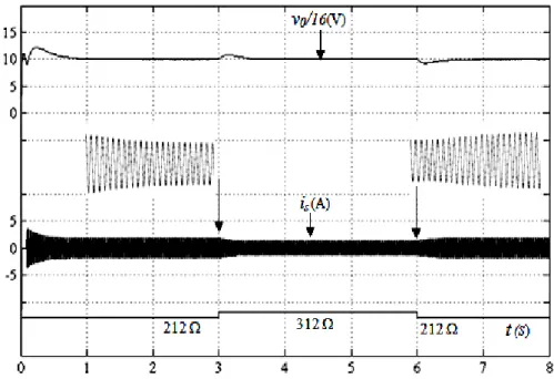
31 Fig.2.10 shows simulations results of the transient response for the proposed PI_Hysteresis control for single-phase power factor correction for a load resistor step from 212Ω to 312 Ω and from 312Ω to 212 Ω. After a short transient, the dc-bus voltage is maintained close to its reference value with a good approximation and stability. The line currents have nearly sinusoidal waveforms and in phase with the input voltage. The corresponding transient values are shown in table 2.2.
The dynamic behavior of the proposed PI_Hysteresis under a step change of V*0 is presented
in Fig.2.11. After a short transient, the dc-bus voltage is maintained close to its new reference with good approximation and stability. The line currents have nearly sinusoidal waveforms. The corresponding transient values are shown in table 2.3.
In the Fig. 1.12 the transient of the step change of vs, by decreasing from 150 V to 140 V and
increasing from 140 V to 150 V of the dynamic behavior of the proposed PI_Hysteresis. After a short transient, the dc-bus voltage is maintained close to its new reference with good approximation and stability. The line currents have nearly sinusoidal waveforms. The corresponding transient values are shown in table 2.4.
Fig.2.7 Simulated basic signal waveforms in steady state under UPF, with FBH, V*0=160 V, THD=3.98%
32 Fig.2.8 Simulated basic signal waveforms in steady state
. under UPF, with SBH, V*0=160 V, THD=3.17%.
Fig.2.9 Simulated basic signal waveforms in steady state under UPF, with variable Band, V*0=160 V, THD=2.01%.
33 Fig.2.10 Transient of the step change of the load Increasing
from 212Ω to 312Ω and Decreasing from 312 Ω to 212Ω.
Fig. 2.11 Transient of the step change of V*0, Increasing
34 Fig. 2.12 Transient of the step change of vs, decreasing
from 150 V to 140 V and increasing from 140 V to 150 V. Table 2.2
Transient values corresponding to Fig 2.10.
Load V0 (V) t (S) Iref (A) t (S)
212Ω/312Ω 12.8 0.7 0.52 0.5
312Ω/212Ω 12.8 0.7 0.52 0.5
Table 2.3
Transient values corresponding to Fig 2.11.
V*0 V0 (V) t (S) Iref (A) t (S)
160V/192V 32 0.8 0.7 0.8
192V/160V 32 0.8 0.7 0.8
Table 2.4
Transient values corresponding to Fig 2.12.
vs V0 (V) t (S) Iref (A) t (S) 150V/140V 3.2 0.8 0.18 0.7 140V/150V 3.2 0.6 0.18 0.71 v0 /16 (V) is (A) 150 V 140 V 150 V t (S)
35 2.5. CONCLUSION.
In this chapter, the design constraints of power-factor-correction power supplies that use a PI-Hysteresis control to achieve high power factor and fast regulation have been study. In addition, the small-signal model of the proposed converter was developed, from witch an optimal PI compensator is designed for the converter system with peak-current mode control. However, the input current harmonic content is very close to the limit specified in IEEE6519 Standard. The static performances of the variable band hysteresis controller are compared to those of the Fixed band hysteresis controller. The results show that the VBH control has THD of the input current much better then with the fixed band hysteresis control.
REFERENCES.
[1]. Yu Qin, Shanshan Du. ―Fuzzy logic and digital PI control of single phase power factor pre-regulator for an online UPS-a comparative study” Industrial Technology, 1996. (ICIT apos; 96), Proceedings of The IEEE International Conference on Volume, Issue, 2-6 Dec 1996 pp. 103 – 107.
[2]. Ahmed H. Mitwali, Steven B. Leeb, George C. Verghese and V. Joseph Thottuvelil. “An Adaptive Digital Controller for a Unity Power Factor Converter,” IEEE Transaction on Power Electronics, vol. 11, no. 2, pp. 374–382, March 1996.
[3]. Simon Wall and Robin Jackson. “Fast Controller Design for Single-Phase Power-Factor Correction Systems,‖ IEEE Transaction on Industrial Electronics, vol. 44, no. 5, pp. 654–660, October 1997.
[4]. Tsai-Fu Wu and Yu-Kai Chen. “Analysis and Design of an Isolated Single-Stage Converter Achieving Power-Factor Correction and Fast Regulation,‖ IEEE Transaction on Industrial Electronics, vol. 46, no. 4, pp. 759–767, August 1999.
[5]. Jee-Woo Lim and Bong-Hwan Kwon. “A Power-Factor Controller for Single Phase PWM Rectifier,‖ IEEE Transaction on Industrial Electronics, vol. 46, no. 5, pp. 1035– 1037, October 1999.
[6]. Zaohong Yang and Paresh C. Sen. “A Novel Technique to Achieve Unity Power Factor and Fact Transient Response In Ac-to-Dc Converters,‖ IEEE Transaction on Power Electronics, vol. 16, no. 6, pp. 764–78, Novembre 2001.
[7]. Fu M. Chen Q. “Applied Power Electronics Conference and Exposition‖, 2001, APEC, 2001, Sixteenth Annual IEEE Volume 1, Issue, 2001 pp. 144 - 149 vol.1.
[8]. [8] Masashi Ochiai and Hirofumi Matsuo. “An AC/DC Converter with High Power Factor,‖ IEEE Transaction on Industrial Electronics, vol. 50, no. 2, pp. 356–361, April 2003.
[9]. [9] L.Rahmani, F.Krim, A.Bouafia. “Deadbeat Control for PWM AC Chopper,‖ Taylor & Francis, Electric Power Components and systems, 32:453-466, 2004.
[10]. [10] L.Rahmani, F.Krim, M.S.Khanniche, A.Bouafia. “Control for PWM AC Chopper feeding nonlinear loads,‖ Taylor & Francis, INT. J. ELECTRONICS, Vol 91, No 3, March 2004, 149-163.