HAL Id: tel-01467109
https://tel.archives-ouvertes.fr/tel-01467109
Submitted on 14 Feb 2017
HAL is a multi-disciplinary open access
archive for the deposit and dissemination of sci-entific research documents, whether they are pub-lished or not. The documents may come from teaching and research institutions in France or abroad, or from public or private research centers.
L’archive ouverte pluridisciplinaire HAL, est destinée au dépôt et à la diffusion de documents scientifiques de niveau recherche, publiés ou non, émanant des établissements d’enseignement et de recherche français ou étrangers, des laboratoires publics ou privés.
sensitized solar cells
Alexandra Szemjonov
To cite this version:
Alexandra Szemjonov. Mixed experimental/theoretical study of quantum dot sensitized solar cells. Chemical Physics [physics.chem-ph]. Université Pierre et Marie Curie - Paris VI, 2016. English. �NNT : 2016PA066301�. �tel-01467109�
T
HESE DE DOCTORAT DE
L’U
NIVERSITE
P
IERRE ET
M
ARIE
C
URIE
M
IXED EXPERIMENTAL
/
THEORETICAL STUDY OF QUANTUM DOT
SENSITIZED SOLAR CELLS
Préséntée le 22 Septembre 2016 par
A
LEXANDRA
S
ZEMJONOV
Pour obtenir le grade de
Docteur de l’Université Pierre et Marie Curie
Ecole doctorale de Chimie Physique et Chimie Analytique de Paris Centre
(ED388)
Devant un jury composé de :
Pr. Alexis Markovits Professeur – Université Pierre et Marie Curie Président du jury
Pr. Régis Gautier Professeur – Ecole Nationale Supérieure de Chimie de Rennes
Rapporteur
Pr. Thierry Toupance Professeur – Université Bordeaux 1 Rapporteur
Dr. Pascal Boulet Maître de Conférences-HDR - Aix-Marseille Université
Examinateur
Dr. Peter Reiss Chercheur – CEA Grenoble Examinateur
Dr. Sandrine Ithurria Maître de Conférences – Ecole Supérieure de Physique et de Chimie Industrielles
Examinatrice
Dr. Thierry Pauporté Directeur de Recherche – Institut de Recherche de Chimie Paris
Directeur de thèse
Dr. Frédéric Labat Maître de Conférences - Institut de Recherche de Chimie Paris
A
CKNOWLEDGEMENTS
I owe my sincere thanks to many people without whom the realization of this work would not have been possible.
First of all, I am much obliged to my thesis supervisors Thierry Pauporté and Frédéric Labat who attentively coordinated my work and who were always available when I needed help or advice. I would like to thank Ilaria Ciofini for her invaluable support, insights and feedback on my work.
I am indebted to my fellow Master, PhD students and postdocs in Chimie ParisTech who I met in the last three years: Jasmina, Diane, Chloé, Liam, Ashwani, Stefania, Luca, Indira, Chiara, Stefania, Vinca, Davide, Marianna, Li, Alistar, Marta, Malvina, Federica, Cecilia, Alessandra, Enzo, Daria, Vincenzo, Antonio, Valentino in the CTM lab, and Sana, Jie, Yuly, Mongia, Ricardo, Maria, Pengjiu, Zhipeng, Suchinda, Karmel, Mariem, Dorra, Akiko, Deborah, Jadwiga, Fanny, Natalie, Sacha, Atul, Jenny, John, Jinlei, Federico, Simon in the MPOE and other labs of the school, and the list is probably not even exhaustive. I received a lot of scientific and friendly help from you, and we spent many great moments inside and outside of the school. I owe many thanks to Patrick for his help with informatical problems, Jean-François for his technical support, Odile for her help and advice in Raman spectroscopy, and the secretaries of the school who helped me out of many administrative problems: Catherine, Ikrame, Elisabeth and Matinou.
I acknowledge Benoit Dubertret for welcoming me in the LPEM lab at ESPCI for the synthesis of nanoplatelets and quantum dots. Special thanks go to Sandrine Ithurria for teaching me the synthesis methods and for useful discussions. I would like to thank Armel Descamps-Mandine for his help and endless patience with the long SEM experiments. I am grateful to the the lab’s PhD students, postdocs and other researchers: Nicolas Lequeux, Silvia, Chloé, Djamila, Emmanuel, Brice, Mariana, Anusuya, Aude, Michel, Fatima, Gary, Sophie and Thomas for their help with the experiments and solving technical problems, as well as for creating a cheerful ambiance in the lab with lots of music.
I owe a lot to my Parisian friends, some of whom already moved abroad, but we still keep in touch: Liping, Sijie, Javier, Mariana and Andreea. Your optimism, open-mindedness and creativity are an endless source of inspiration for me. I am grateful to have my Hungarian friends who can always cheer me up even from a large distance, and who enlighten all my visits back to my home country: Zsófi, Évi, Kati and Panni.
It is needless to say that I have no words to express my gratitude towards my family all over Europe, especially my sister Krisztina and my mother for their solid support, encouragement and love.
A
BSTRACT
The general aim of this thesis was to contribute to a better understanding of the procedures governing the performance of quantum dot sensitized solar cells. A mixed theoretical/experimental approach was used to analyze the semiconductor components of these devices and the interfaces formed between them. Regarding the theoretical part of this thesis, we first identified a computational protocol that accurately and efficiently describes the bulk and surface geometrical and electronic properties of the chosen sensitizer material, CdSe. Then, we simulated CdSe nanoplatelets of various thicknesses, passivated by different ligands with the chosen computational protocol. Next, a model of the sensitizer - wide band gap semiconductor heterostructure was built and its structural, vibrational and electronic properties were calculated. In the meantime, computational results were compared to experimental data, with nice agreements found between the results obtained by the two approaches. Experimentally, wide band gap semiconductors both in the form of ZnO and TiO2 nanorod arrays and sensitizer nanocrystals (CdSe nanoplatelets and quantum
dots) were synthesized. The WBSC substrates were sensitized both by ex situ and in situ grown CdSe QDs. The as-prepared semiconductor systems were characterized by UV-VIS absorption and Raman spectroscopy. Finally, solar cells based on these heterostructures were fabricated and tested. The applied combined theoretical/experimental approach made it possible to cross-validate the capacity of computational and experimental methods for the characterization of the semiconductor systems studied in this thesis. Moreover, general guidelines for the screening of QDSC components could be drawn from the obtained results. The here proposed mixed theoretical/experimental approach can be extended to other semiconductor heterostructures in a wide variety of optoelectronic applications, and it could contribute to a better understanding of the working principle of these devices and improve their performance.
R
ESUME
Le but général de cette thèse était de mieux comprendre les procédures qui gouvernent la performance des cellules solaires à boîtes quantiques. Une approche mixte théorique/expérimentale a été utilisé pour analyser les composants semi-conducteurs de ces dispositifs, ainsi que les interfaces qui se forment entre eux. En ce qui concerne la partie théorique de cette thèse, tout d’abord on a identifié un protocole computationnel qui décrit d’une façon précis et efficace les propriétés géométriques et électroniques du bulk et les surfaces de CdSe, ce qui est le matériau qu’on a choisi comme composé sensibilisant de nos cellules solaires. Après, les nanoplaquettes CdSe de plusieurs épaisseurs et passivé par plusieurs ligands distincts ont été simulés avec le protocole computationnel choisi. Ensuite, une hétéro-structure sensibilisant – semi-conducteurs à large bande interdite a été modélisée, et ses propriétés structurelles, vibrationnelles et électroniques ont été calculées. En même temps, les résultats théoriques étaient comparés avec les données expérimentales, et des accords satisfaisants ont été trouvés entre les deux approches. Expérimentalement, des semi-conducteurs à large bande interdite sous le forme des nanobatôns de ZnO et de TiO2, ainsi que des nanocristaux sous forme des nanoplaquettes et
des boîtes quantiques CdSe ont été synthétisées. Les nanobatôns ont été sensibilisés à la fois avec des nanocristaux CdSe préparés ex situ et in situ. Les systèmes semi-conducteurs ainsi préparées ont été caractérisées par spectroscopie d’absorption UV-VIS et Raman. Enfin, des cellules solaires incorporant ces hétérostructures semi-conducteurs on été fabriquées et testées. L’approche combiné expérimentale/théorique qu’on a utilisée dans cette thèse a rendu possible de contre-valider la capacité des méthodes expérimentales et théoriques pour caractériser les systèmes semi-conducteurs étudiées lors de cette thèse. De plus, on a pu établir des indications générales pour la sélection des composants pour les cellules solaires à boîtes quantiques. L’approche mixte expérimentale/théorique présentée dans ce manuscrit peut être étendu pour étudier des hétérostructures semi-conducteurs dans une vaste gamme des applications optoélectroniques, et peut contribuer à mieux comprendre leur fonctionnement et à améliorer leur performance.
T
ABLE OF CONTENTS
Chapter I CONTEXT………..……… 1
I.1. Global energy trends………..…….……… 1
I.2. Photovoltaic technology………..…….……… 2
I.3. Quantum dot sensitized solar cells……….. 5
I.3.1. Working principle……….. 8
I.3.2. Components………. 8
I.3.2.1. Quantum dots………. 8
I.3.2.2. Wide band gap semiconductors………..…….……… 10
I.3.2.3. Transparent conductive oxide glass………. 11
I.3.2.4. Electrolytes……… 12
I.3.2.5. Counter electrodes……….……… 14
I.4. Solar spectra……….…….……… 14
I.5. Solar cell efficiency factors……….…….……… 15
I.6. State of art……….……… 17
I.6.1. Experimental challenges……….. 17
I.6.2. Modeling challenges……… 19
I.7. Goals and outline of the thesis……… 23
References………. 25
Chapter II THEORETICAL AND EXPERIMENTAL METHODS………..….……… 33
II.1. Theoretical methods………….……… 33
II.1.1. The Schrödinger equation ……… 33
II.1.2. Hartree-Fock method……… 35
II.1.3. Density functional theory……….………….. 39
II.1.4. The Kohn-Sham method……….………. 40
II.1.5. Exchange-correlation functionals……….……….. 42
II.1.6. Modeling periodic systems……… 44
a) Bulk crystals………..……… 44
b) Crystal surfaces………..…… 47
II.1.6. Basis sets for periodic DFT calculations………...…… 48
a) Localized basis sets……….. 48
b) Plane wave basis sets………. 50
II.2. Experimental methods………. 52
II.2.1. Synthesis of CdSe nanoplatelets and quantum dots……… 52
II.2.2. Synthesis of 1D wide band gap semiconductor nanostructures……….….… 55
a) ZnO nanorods………..…… 56
b) TiO2 nanorods………..… 60
II.2.3. Attachment of quantum dots to wide band gap semiconductors…………..……… 63
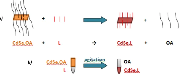
a) Sensitization by linker-assisted attachement……….………..… 63
b) Sensitization by the SILAR method……… 66
II.2.4. Assembly of solar cells………..……… 68
a) All-solid-state QDSCs……….. 68
b) QDSCs with liquid electrolyte……… 69
References………. 72
Chapter III BULK AND SURFACE PROPERTIES OF CDSE……… 78
III.1. Context……….……… 78
III.2. Computational details……… 79
III.3. Bulk properties of CdSe……….……… 81
III.3.1. Structural features……… 81
III.3.2. Energetics and electronic properties……….. 84
III.4. Surface properties of CdSe………. 90
III.4.1. Geometrical properties………. 90
III.4.2. Electronic properties……….. 92
III.5. Conclusion……….. 94
References………. 96
Chapter IV CADMIUM SELENIDE NANOPLATELETS……… 99
IV.1. Context………. 99
IV.2. Experimental details……… 99
IV.3. Computational details……… 100
IV.4. Theoretical model of the CdSe zinc blende (100) surface………. 102
IV.5. Geometrical investigation……… 104
IV.6. Adsorption energies……… 107
IV.7. Electronic properties……….. 108
IV.8. Conclusions……… 114
References………. 116
Chapter V HYBRID SEMICONDUCTOR HETEROSTRUCTURES………. 118
V.1. Context………. 118
V.2. ZnO and TiO2 nanorod arrays……… 119
V.3. Attachment of CdSe nanoplatelets to WBSC via SH- ligands……….. 122
V.4. Attachment of CdSe nanoplatelets to WBSC via OH- ligands………. 128
V.5. Attachment of CdSe nanoplatelets to WBSC via MPA ligands………..………… 130
V.6. Attachment of CdSe quantum dots to WBSC………. 133
V.7. Conclusion……….. 134
References………. 136
Chapter VI TOWARDS THE MODELING OF QDSCS: SENSITIZER – OXIDE HETEROSTRUCTURES……….. 138
VI.1. Context………. 138
VI.2. Experimental details……….. 139
VI.3. Computational details……… 140
VI.4. Structural features of the CdSe.SH – ZnO system……….. 142
VI.5. Vibrational features………..……….. 146
VI.6. Electronic properties……….. 155
VI.7. Conclusions……… 158
References………. 161
Chapter VII QUANTUM DOT SENSITIZED SOLAR CELLS………. 163
VII.1. QDSCs based on ex-situ prepared CdSe nanocrystalss……… 163
VII.1.1. All-solid-state QDSCs……….. 163
VII.1.2. QDSCs with liquid electrolytes………. 165
a) ZnO-based QDSCs………. 165
VII.2. QDSCs based on in-situ prepared CdSe QDs……….. 166
VII.2.1. QDSCs with a ZnO substrate……….. 167
VII.2.2. QDSCs with a TiO2 substrate………..……….. 175
VII.3. Conclusion……….. 178
References………. 181
CONCLUSIONS AND PERSPECTIVES………. 182
PUBLICATIONS RELATED TO THE THESIS……… 187
PRESENTATIONS AT SCIENTIFIC EVENTS………. 187
LIST OF FIGURES……… 189
LIST OF TABLES………. 195
ANNEXES ……….. 197
Annexe I. Geometrical and electronic properties of the CdSe.SH (9L) – ZnO system….. 197
I.1. Global energy trends
At present, nearly 80% of the yearly energy consumption of 5.67∙1020 J/year which is
equivalent to a total of ≈18 terawatts (TW)1 is provided by fossil fuels such as coal,
petroleum and natural gas.2 Although the U.S. Energy Information Administration (EIA)
predicts a 56% growth in global energy consumption by 2040,3 the fossil energy sources can
still account for the increased global energy demands at least until 2050.4 However, as fossil
fuels are converted to energy, they produce greenhouse gases (such as carbon dioxide, methane and nitrous oxide) and other harmful pollutants (ash, sulphur oxide etc.). The use of fossil fuels thus contributes to global warming, as it has been pointed out in the Fourth Assessment Report of the Intergovernmental Panel on Climate Change (IPCC),5 and the
deterioration of the quality of air. If the global energy demand continues to be satisfied by fossil energy sources at the present rate, the atmospheric CO2 concentration could rise
above 685 ppm, which would lead to a 3-6 °C rise in global average temperature,6 and have
catastrophic consequences on the climate and the environment.
Consequently, more and more effort has been invested in the last decades into the research of alternative, environmentally friendly and renewable energy sources. In 2014, for the first time in 40 years and despite the increasing energy use, global carbon emissions associated with energy consumption remained stable while the economy grew, which is attributed to the increasing use of renewable energy sources.7 Solar energy is by far the most exploitable
choice among them: 3.85∙1024 J/year, equivalent to a power of 120000 TW/year energy
reaches the Earth from the Sun, 8 which is four orders of magnitude larger than the current
global energy use. In comparison, the yearly maximum energy supply of other renewable energy sources is only a small fraction of that of solar energy: 1.5 TW/year is exploitable from hydroelectric power, 2 TW/year energy from tides and ocean currents, 2-4 TW/year from wind power and 12 TW/year from geothermal energy.9,10 However, in order to make
solar energy a widespread energy source, scalability, cost and conversion efficiency issues need to be solved.11,12
I.2. Photovoltaic technology
Photovoltaic (PV) technologies aim at the direct conversion of solar energy into electricity. The classical way is based on the photovoltaic effect: the creation of voltage and electric current upon exposure to light in an assembly of a p- and a n-type material in close contact, forming a p-n junction. p- and n-type materials are derived from the bulk material by doping it with electron acceptors or donors, respectively. For instance, silicon can be made p-type (n-type) by doping with atoms that contain less (more) valence electrons than silicon, for example with aluminium (phosphor).
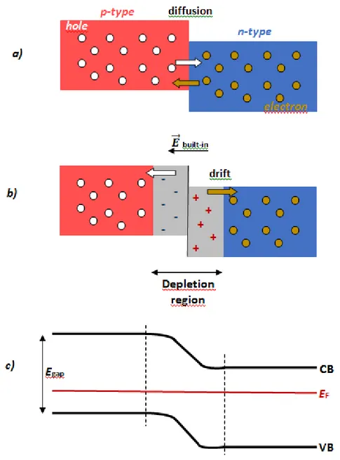
Two important semiconductor characteristics are defined in Figure I.1 c). The band gap (Egap)
is the minimal energy required to excite an electron from its bound state in the valence band (VB) into a free state in the conduction band (CB). The Fermi level (EF) represents the
chemical potential of the electrons. While the EF is in the middle of the band gap in an ideal
intrinsic (non-doped) semiconductor, it is closer to the top of VB (bottom of CB) in a p-type (n-type) semiconductor.
In the p-n junction, the n-type region has a high electron concentration, and the p-type region has a high hole concentration. Therefore, when the two semiconductors are put in contact, electrons from the n-type side diffuse freely to the p-type side. Similarly, holes diffuse from the p- to the n-type region (Figure I.1 a) ). This diffusion of the charge carriers through the junction causes a diffusion current. The free charge carriers are quickly swept out from the area around the junction, which is thus called depletion region (Figure I.1 b) ). These displaced electrons and holes leave behind charged dopant atom sites fixed to the crystal lattice: positive ion cores are left behind in the n-type, and negative ion cores in the
p-type material, forming an electric (built-in) field, which works against the above described
charge diffusion, and sweeps back the electrons and holes that are trying to cross the depletion region, causing a drift current.
In equilibrium, the electron drift and diffusion current, as well as the hole drift and diffusion
applied to the p-type, and a negative voltage to the n-type region, an electric field opposing the built-in field of the depletion region is applied across the device, and the diffusion current is increased. This is called forward bias. In case of reverse bias, a voltage is applied across the device such that the built-in field increases, and the diffusion current decreases.
Figure I.1. a) Diffusion of free charge carriers between a p- and an n-type material. b) Formation of a depletion region with a built-in electric field in a p-n junction. c) Band energy levels in the p-n junction.
There are two major processes leading to a current generation in p-n semiconductor
of the incident light is equal or superior to the band gap, electrons are promoted from the VB to the CB, leaving holes behind in the VB, and electron-hole pairs are thus created. The second process is the collection of charge carriers. The built-in field in the depletion region spatially separates the electrons and the holes and thus prevents recombination. Electrons and holes are driven towards different collectors, and if the terminals of the p- and n-type material are connected, the charge carriers can leave the device, and flow through the external circuit: a photogenerated current has been created.
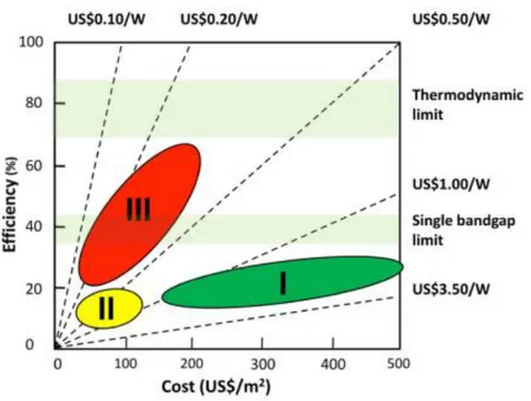
Figure I.2. First, second and third generation photovoltaic cells. Adapted from Ref. 13
One of the most commonly used classifications of single junction photovoltaic solar cells is based on the cost-efficiency relationship, as illustrated in Figure I.2. Currently first
generation solar cells made of crystalline silicon dominate the commercial market, although
the high purity of the initial material makes them expensive.14 Also, silicon has an indirect
band gap with a low absorption coefficient, which implies the use of thick absorber layers in the devices. Second generation thin film PV technologies exploit simpler/cheaper industrial processes and offer larger scaling module integration (potentially of flexible substrates), much lower materials consumption/cost plus reduced payback time compared to crystalline silicon (c-Si) based technologies.15 Currently amorphous/microcrystalline (a/m-Si) silicon,
CdTe and Cu(In1-xGax)S2-ySey (CIGSSe) based technologies dominate the thin film PV market.
Whilst a-Si cells suffer from relatively low conversion efficiency (the best laboratory power conversion efficiency [PCE] is 13.4% measured at Sharp), thin film CdTe offers a record PCE of 22.1% (First Solar), and CIGSSe offers a record PCE of 22.3% (Solar Frontier).16 Despite the
improvement with respect to first generation solar cells, second generation solar cells in general still require relatively costly high purity materials and some of them are based on rare resource elements, prepared with tedious and complicated processing conditions, Third
generation solar cells gather new solar cell concepts which are very low cost and/or have a
very high efficiency. They include multijunction solar cells, organic photovoltaic cells and also organic/inorganic or inorganic/inorganic hybrid devices, such as dye-, quantum dot (QD)- and perovskite-sensitized solar cells. The main advantages of the new concept third
generation devices include low-cost materials and fabrication techniques,17 and the
possibility to overcome the theoretical efficiency limit of single junction devices18
established by Schockley and Queisser. They obtained a maximum power conversion efficiency of 31% for a semiconductor single junction with a band gap of 1.4 eV.19 Their
calculation was based on the following assumptions. 1) Every incident photon with an energy greater than or equal to the band gap of the semiconductor produces one electron-hole pair.
2) The photon energy above the band gap is converted to heat (thermalization loss). In
reality, the efficiency of solar cells is lower than the ideal calculated value, mainly due to light reflection, non-radiative charge recombinations and ohmic losses.
I.3. Quantum dot sensitized solar cells
I.3.1. Working principle
The novelty of hybrid solar cells compared to first and second generation solar cells is that the different steps of the photovoltaic procedure (light absorption, charge separation and charge transport) are realized in different materials, and can thus be optimized separately. The components of QDSCs will be described in more detail in section I.6. In brief, QDSCs are composed of an n-type wide band gap semiconductor (WBSC, typically ZnO or TiO2) of large
heterostructure is grown on a transparent conductive oxide (TCO) coated glass. The TCO layer is usually made of fluorine doped tin oxide (SnO2:F), denoted as FTO. The cell is
completed by an electrolyte which contains a redox couple (typically S2-/S
n2-) and a counter
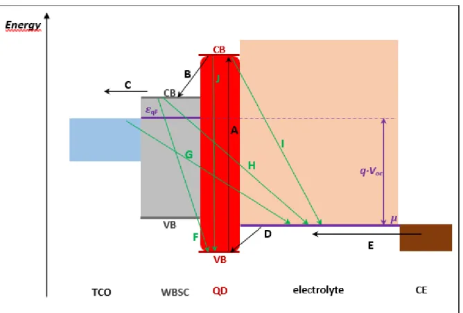
electrode (CE). The working principle of these devices is also illustrated in Figure I.3, and the schematic illustration of the charge generation, transfer and recombination processes is reported in Figure I.4.
The absorption of light excites an electron from the VB to the CB of a QD (procedure A on
Figure I.4.). Then, it is injected to the CB of the WBSC (B), which increases the Fermi level of
the WBSC. This upshifted, out-of-equilibrium energy level is called quasi-Fermi level, and is denoted as Eqf on Figure I.4. In the next step, the WBSC transfers the excited electrons
towards the FTO layer of a glass substrate (C). The FTO-coated glass leads the photogenerated electrons towards the external circuit. The oxidized QD is regenerated by hole injection from a redox species present in the electrolytic solution (D), characterized by its redox potential (µ). As illustrated in Figure I.4., an important solar cell parameter, the open circuit voltage (Voc) is defined as the difference between the quasi-Fermi level of the
WBSC and the redox potential of the electrolyte:
Voc = Eqf - µ (I.1)
The electrolytic solution is then regenerated by reduction at the counter electrode (E). The main parasitic recombination pathways that decrease the device performance occur between electrons already injected to the WBSC and holes left in the QD (F), electrons in the TCO and holes in the electrolyte (G), electrons already injected to the WBSC and holes in the electrolyte (H), and electrons in the QD and holes in the electrolyte (I). Another possible recombination phenomenon can occur if the QD gets back to its initial state before injecting the electron to the CB of the metal oxide (J).
Figure I.3. Working principle of quantum dot sensitized solar cells. The scheme at the bottom shows the electron injection from the quantum dot to the semiconductor oxide.
Figure I.4. Main charge generation, transfer and recombination processes in a QDSC. Favorable electron transfer procedures are marked with a black. Undesired electron-hole
I.3.2. Components
I.3.2.1 Quantum dots
Quantum dots (QDs) are typically II-VI, III-V or IV-VI semiconductor nanocrystals whose size is in the order of a few nanometers in all dimensions. Most common materials investigated as QDs include CdS20, CdSe21, CdTe22, PbS23, PbSe24, Bi
2S325, Sb2S326, InAs27 and CuInS228
quantum dots. Their nanometric size is comparable to their Bohr exciton radius (ab), which is calculated according to the following equation:
(I.2)
where is the reduced Planck constant, ε is the dielectric constant of the material, e is the electronic charge, and are the effective masses of electrons and holes, respectively. Physically, the Bohr radius represents the average electron-hole distance in an exciton, which is an electron-hole pair bound by Coulombic forces. Excitons are created in the semiconductor material upon the absorption of a photon with an energy greater than or equal to the semiconductor band gap. Once the diameter of a material is smaller than its Bohr radius, the excitons become so strongly bound that they can be considered as an entity moving in the crystal lattice. However, their movement is strongly limited by the size of QDs, or, in other words, they are spatially confined in 3 dimensions. In case of 1 dimensional (1D) nanoobjects like nanowires/nanorods, these quantum confinement effects arise in 2 dimensions, and in case of quasi-2 dimensional (2D) objects such as nanoplatelets, they occur only in 1 dimension. The quantum confinement effect has a strong impact on the energy level distribution: the band gap of nanoobjects increases with decreasing size, and their energy levels become more discretized. These are both very advantageous properties for photovoltaic applications, as explained in the following.
Tuning the band gap energy of the light absorbing component of quantum dots is an important step in optimizing the solar cell performance. Too low a band gap results in efficiency losses due to the thermalization of the photon energy excess with respect to the sensitizer’s band gap energy. In the case of high band gap, a large proportion of the photons of the incident light is not absorbed, since their energy is inferior to that of the quantum dot’s band gap. Based on Shockley and Queisser’s calculations, for a single junction, these losses are minimal at a band gap of around 1.3-1.4 eV.19 However, to optimize photovoltaic
conversion, it would be desirable to absorb light in the whole solar spectra. This could actually be possible by combining QDs with several band gap energies.29 The development of
synthesis methods has made it possible to fine tune the nanoparticle size and thus the band gap of various quantum dot materials, making the engineering of solar light absorption possible.30–32
The discretization of energy levels could also make it possible to exceed the Shockley-Queisser efficiency limit. If a photon with an energy greater than the band gap of the semiconductor materials is absorbed, an electron-hole pair with excess kinetic energy is generated first. These carriers are called hot electrons and hot holes. In a bulk material with a continuum of electronic states, they are relaxed to the top of VB or the bottom of CB by collective vibration of the interacting atoms in the system (phonon emission). However, the discretization of energy levels slows down the relaxation process, especially if the distance between the energy levels is higher than the phonon energies. This phenomenon called
phonon bottleneck facilitates generating a current of hot carriers before they are relaxed.
Two approaches have been proposed to exploit the high energy of hot carriers. In the first one, hot carriers are extracted before their thermalization, and a higher photocurrent can be generated by the device. This phenomenon called hot electron transfer has been observed for instance between PbS QDs and a TiO2 single crystal.33 Moreover, Lee et al. demonstrated
making use of hot carriers in a complete photovoltaic device.34 In the second approach, if the
incident photon energy is at least two times higher than the band gap, the energy released during the relaxation of hot carriers can theoretically create new excitons, which results in an increased current. This is called multiple exciton generation (MEG). Multiple electron transfer has been reported between MPA-capped CdSe QDs and ZnO nanowires.35 Beard and
heterojunction solar cell based on PbSe QDs and ZnO.18 However, taken all together, these
promising concepts have brought little improvement in device efficiency, since their application to actual solar cells requires a very high control level of the interfaces.36
Among the above listed QD materials, cadmium chalcogenides have attracted considerable attention because of their easy, low fabrication cost,37–39 controllable size,40,41
photostability42 and also the possibility to break the Schockley-Queisser limit via multiple
exciton generation.43,44 In this thesis, we have concentrated on CdSe nanocrystals, which had
previously been synthesized in various shapes: spherical nanoparticles,45 nanorods (NRs)46,
nanoribbons,47 tetrapods48, nanosheets49 and nanoplatelets50. Regarding the latter, CdSe
zinc blende nanoplatelets (NPLs) are versatile structures which can be fabricated with a well-defined thickness controlled at an atomic scale in the (100) direction.40 These quasi
two-dimensional nanocrystals have been proven to be useful for a broad range of applications ranging from single-photon sources51 to biophotonics52. Compared to QDs and NRs, they
show much narrower excitonic absorption and photoemission bands50,53 and higher
photoluminescence quantum yields.54 Taken all together, quasi two-dimensional
nanoplatelets exhibit promising properties for photovoltaics, and are interesting alternatives of QDs as sensitizers. Although classical spherical QDs as sensitizers have also been considered in this thesis, we mainly focused on quasi two-dimensional semiconductor nanoplatelets (NPLs).
I.3.2.2 Wide band gap semiconductors
In QDSCs, QDs are associated to a selective contact which is classically made of a wide band gap semiconductor (WBSC). The role of this component is to receive the electrons from the QD conduction band after electron injection, and to transport charges to the front FTO contact. As the QDs are the only light absorbing components of the cells, a selection criteria for WBSCs is that their band gap is wide enough so that its absorption range does not overlap with the solar spectrum. In order to ensure the efficient electron injection from the sensitizer towards the WBSC, the CB edge of the WBSC material needs to be at lower energy compared to the sensitizer CB edge energy. ZnO and TiO2 meet these requirements if paired
These materials have band gaps (3.2055 for TiO
2 and 3.37 eV56 for ZnO) and also CB band
positions.57 Although TiO
2 is more used in QDSCs than ZnO, the latter has some more
advantageous properties. It has a higher electron mobility (200-300 cm² V s-1) than TiO 2
(0.1-4 cm² V s-1)57, and it is easier to synthesize in highly oriented nanostructures.58–60 As high
QDSC efficiencies have been reached both with ZnO-61,62 and TiO
2-based photoanodes,63,64
both semiconductors were considered in this thesis.
It has been shown for dye sensitized solar cells that increasing the WBSC surface area, and thus increasing the amount of sensitizers adsorbed on the WBSC leads to higher IPCE values.65,66 Numerous different kinds of nanostructured ZnO and TiO
2 nanostructures
morphologies with high surface area have thus been synthesized, including nanoparticle films and more exotic ones such as DNA-like,67 flower-like68,69 or hierarchical spherical
nanoarchitectures.70 One dimensional nanostructures like nanorods, nanowires and
nanotubes are precisely oriented, therefore they provide excellent charge streaming pathways71–73 and an improved electron diffusion length with respect to nanoparticle
films.74,75 It is also to note that the transported electrons in the commonly used nanoparticle
films suffer charge trapping and recombination losses at the grain boundaries,76,77 whereas
this phenomenon is reduced in the case of one-dimensional nanostructures.78–80 As a result,
charge transport and photon-to-charge carrier generation efficiency are significantly increased with respect to devices incorporating nanoparticle-based photoanodes.30,81 In this
thesis, we thus chose to synthesize ZnO and TiO2 in the form of 1D nanorods and nanowires.
I.3.2.3. Transparent conductive oxide glass
The wide band gap semiconductor is grown on a conductive layer deposited on the side of a glass substrate (Figure I.3.). The conductivity of this layer is necessary to ensure a good electron transport towards the external circuit, while high transparency is required to let the incident light reach the sensitizer of the cell. In most cases, the conductive layer is made of fluorine doped tin oxide (SnO2:F, FTO), although tin-doped indium oxide (In2O3:Sn, ITO) has
also been used in several studies.82,83 The thicker this layer is, the more conductive it is,
parameters. In the present thesis, 2.2 mm thick glass substrates coated with a FTO layer of 15 ohms per square resistance were used for the preparation of the photoanodes.
I.3.2.4. Electrolytes
As the I-/I
3- redox couple applied in dye-sensitized solar cells causes the photocorrosion of
typically used QD materials such as cadmium chalcogenides,84,85 alternative electrolytes have
been developed to replace it. The most commonly used redox electrolyte for QDSC application is the sulfide/polysulfide (S2-/S
n2-) electrolyte, which have been shown to
increase the photoanode stability because of the formation of a cadmium sulfoselenide layer on the QD’s surface.86 Other redox electrolytes, including Co2+/Co3+ 87 and
ferricyanide/ferrocyanide88 have also been investigated.
The hole transporting role of the redox electrolyte is shown through the example of the sulfide/polysulfide (S2-/S
n2-) electrolyte which was used in this thesis. As the photoexcited
electron is injected from the QD to the WBSC, the holes accumulated in the QD are scavenged by the reduced species (S2-) of the redox electrolyte, which is thus oxidized. (Equation
I.3. The resulting compound (S) is complexed by sulfide anions (Equation I.4), and the
complex species get reduced to the initial sulfide ion in contact with the electrons of the counter-electrode (Equation I.5).84
S2- + 2h+ → S (I.3)
S + nS2- → (S
n+1)2- (I.4)
(Sn+1)2- + 2e- → S2- + Sn2- (I.5)
However, the exact mechanism of the process is still controversial. For example, Kamat et al. observed sulfide radicals as intermediate products of the oxidation-reduction processes.86
The drawback of sulfide/polysulfide redox electrolytes is their relatively high redox potential which limits the open-circuit voltage at around 0.65 V, a value is significantly lower than that achieved in dye-sensitized solar cells (1.0 V) using cobalt redox species.89–92 Decreasing the
charge recombination rate between the photoanode components and the electrolyte is another challenging issue. Du et al. demonstrated that the introduction of well-chosen
additives in the electrolyte solution can reduce recombination phenomena and contribute to a better photovoltaic performance.93
Nevertheless, liquid electrolytes do not provide long-term stability for QDSCs. Solvent evaporation, leakage and corrosion are the major drawbacks related to the use of liquid electrolytes.94,95 Due to these disadvantages, solid-state electrolytes have also been applied
in QDSCs. In these fully solid-state devices, organic molecules or a polymer electrolyte replaces the liquid redox electrolyte. Typical examples of solid-state electrolyte materials applied in QDSCs include poly(3-hexyltiophene-2,5-diyl)96 (P3HT), quatertiophene97 and
2,2’7,7’-tetrakis[N,N-di(4-methoxyphenyl)amino]-9,9’-spirobifluorene (denoted as spiro-OMeTAD)98. Despite the promising concept, solar cells assembled with solid state
electrolytes show much lower performance than those with liquid electrolytes. For instance,
a power conversion efficiency of 1% has been reported for a QDSC based on PbS and CdS QD-sensitized TiO2 and a spiro-OMeTAD electrolyte,99 and 0.3% for a cell based on CdSe
QD-sensitized TiO2 and quatertiophene as hole transporting material (HTM).97 The main reason
for this low performance is probably the incomplete pore filling of the photoanode by HTM.99
Finally, quasi-solid state electrolytes (including gel electrolytes and highly viscous ionic liquid electrolytes) have also been proposed, resulting in higher solar cell efficiencies. For instance, Wang et al. reported a power conversion efficiency of 4.0% for a CdS/CdSe QD-sensitized solar cell with a TiO2 photoanode and a natural polysaccharide (Konjac glucomannan) –based
quasi-solid state electrolyte100 or Karageorgopoulos et al. measured an overall efficiency of
4.5% for solar cells using a CdS/CdSe-sensitized ZnO photoanode and a polysulfide-based ionic liquid.101
Although the expression ‘hole transport material’ is most often applied for solid state
electrolytes, all the above described electrolytes play the same hole transporting role in
hybrid solar cells. Therefore, in the following, solid, quasi-solid state and liquid electrolytes will all be referred to as hole transport materials (HTMs).
I.3.2.5. Counter electrodes
Counter electrodes (CEs) are expected to have a high electrocatalytic activity for the regeneration of the redox couple of the electrolyte, high conductivity and no willingness to react with the rest of the solar cell components. A typical CE in dye-sensitized solar cell (DSSCs) consists of a platinized conducting glass substrate, and is usually referred to as a Pt counter electrode. However, while Pt electrodes are highly catalytic for the reduction of I3- in
the iodine/iodide electrolyte, this is not the case for the sulfide/polysulfide electrolyte. Sulphur compounds tend to chemisorb on Pt surfaces, poison the electrode, and hinder the electrocatalytic effect.102 The high overpotential for the electrolyte regeneration results in
low power conversion efficiencies.103–105 Consequently, a wide variety of other materials
(such as CoS106, Cu
2S104, Au105, PbS107 and Cu2ZnSnSe4108) have been investigated, among
which Cu2S gave the best results.103,104 However, Cu2S counter electrodes have some
drawbacks. With an extended use, they might contaminate the electrolyte and the photoanode.104,106 In case of solid-state QDSCs, a thin layer of Au109,110 evaporated on the
HTM layer is typically applied as a counter electrode. Pt101 and Cu
2S111 CEs have been
combined with quasi-solid state electrolytes.
I.4. Solar spectra
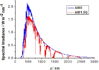
As the actual solar irradiation received by the device is influenced by numerous conditions, such as weather, time of the day, geographic location, latitude, orientation etc., the evaluation of solar cell characteristics and the comparison of different solar cells around the world would be extremely difficult. It was thus necessary to standardize measuring conditions. The currently accepted standards have been established by the American Society for Testing and Materials (ASTM). Figure I.5 shows two important standard spectra, AM0 and AM1.5G. The number in the abbreviation shows the quantity of air mass that the light passes through. Therefore, AM0 stands for Air Mass 0, and corresponds to the spectra after having crossed 0 atmosphere. AM0, is thus used for extraterrestrial applications. The total incident power obtained by the integration of the curve is 1366.1 W m-2 nm-1. Due to scattering and
Earth. AM1 corresponds to the solar irradiance measured at the sea level at the Equator, at a solar zenith angle of z=0°, after having crossed one atmosphere. AM1.5 corresponds to 1.5 atmosphere thickness, at a solar zenith angle of z=48.2°. Therefore, it is a closer approximation to the solar irradiance spectra measured at the world’s densely populated areas at temperate altitudes (North America, Europe, China, Japan, Australia, South Africa). The commonly used AM1.5G spectrum is based on the G173 standard, and is used for terrestrial applications including both diffuse and direct light. By convention, it corresponds to an integrated solar power of 1000 W m-2. The AM1.5D spectrum, also based on ASTM
G173, only includes direct light, and corresponds to an integrated power of 888 W m-2.
Figure I.5. Solar irradiance spectra references according to the ASTM standards.
I.5. Solar cell efficiency factors
In order to evaluate the performance of a solar cell, an external bias is applied to the device, and its current-voltage (I-V) characteristics are measured under illumination and in the dark. The current-voltage (I-V) curve of a typical photovoltaic cell is illustrated in Figure I.6. The most important points of this I-V curve are the short-circuit current (Isc), the open-circuit
current (Voc), the maximum power output (Pm), and the current (Im) and voltage (Vm)
corresponding to Pm. In more detail, Isc is the maximum generated photocurrent, which
corresponds to zero applied voltage. Voc, previously defined in Equation I.1 and Figure I.4., is
It is straightforward to obtain an important solar cell efficiency parameter, the fill factor (FF) from the measured I-V curve. The fill factor evaluates the solar cell performance with respect to its maximum power output (Pm), and it is defined as:
(I.6)
The graphical interpretation is displayed in Figure I.6. FF is thus the ratio of the area defined by the maximum power output (violet dashed lines) and the rectangle defined by Isc and Voc
(green dashed lines). A FF value of 1 corresponds to an ideal cell where all photogenerated carriers are collected, and there are no resistance losses.
Figure I.6. Current-voltage characteristics of a photovoltaic cell under illumination.
The most important device evaluation parameter is the maximum photovoltaic power conversion efficiency. It is defined as the fraction of incident power (Pin) which is converted
(I.7)
The IPCE (incident photon to current efficiency) is the ratio of the charge carriers collected at the electrodes and the number of incident photons. Determining the short-circuit currents at different wavelengths of incident light, we can obtain the IPCE from the following expression:
(I.8)
where Pinc is the incident light power (W cm-2), λ is the wavelength of incident light (in nm),
and Isc is the short circuit current density expressed in A cm-2.
I.6. State of art
I.6.1. Experimental challenges
The first reported complete quantum dot sensitized solar cell dates back to 1998, and was demonstrated by Zaban et al.112. Their QDSC contained nanoporous TiO
2 electrodes
sensitized with InP QDs, and the device was completed with a Pt counter electrode and a I
-/I3- electrolyte solution. As detailed in the previous sections, great progress has been made
since then by finding more suitable materials, such as sulfide/polysulfide based redox electrolytes and Cu2S counter electrodes. It is particularly notable that QDSC efficiencies
doubled in the last 4 years from 5.4%113 to 11.6%,114 and many efficiency improvements
have been achieved by surface treatments of the nanocrystals and of the wide band gap metal oxides. Two important challenges can be addressed with well-chosen surface treatments: 1) alignment of energy levels through surface dipoles on the nanocrystals115 and
2) passivation of trap states at the semiconductor surfaces and interfaces that reduce conductivity and serve as recombination centres.116–118 Trap states at semiconductor
surfaces and interfaces are also responsible for the Fermi level pinning: they pin the Fermi level of the WBSC at a certain energy value within the band gap, which is thus unable to shift
up when the WBSC receives electron injection from the sensitizer. In consequence, the available open circuit voltage (defined on Figure I.4 and in Equation I.1.) will be well below the predicted energy level.119
In the following, a few important milestones achieved since 2014, during the course of this PhD are highlighted. Most of them are oriented towards the surface engineering of the WBSC and QD surface in order to dramatically reduce recombination reactions, as described above, and they also pave the way for future research directions. Wang et al. deposited a Mn-modified CdSe layer on the TiO2/CdSexTe1-x photoanode surface, which acted as a
passivation layer, and also increased the photoanode’s light absorption. Their solar cell reached an efficiency of 8.1%.120 Ren et al. modified the surface of both CdSeTe QDs and of
the mesoporous crystalline TiO2 layer. They deposited a ZnS/SiO2 layer onto CdSeTe QDs,
added an amorphous TiO2 coating on the surface of TiO2 nanoparticles, and reached a power
conversion efficiency of 9.0%.121 They demonstrated in their study that recombination at the
QD-TiO2 interface was reduced due to amorphous TiO2 interlayer. Another approach to
efficiently suppress surface trap states on QDs is to construct core/shell nanocrystals. Yang et al. optimized the CdS shell on CdSeTe cores, and attached them to TiO2 film electrodes.122
They demonstrated that the solar cells based on these photoanodes are significantly more efficient than using plain CdSeTe QDs, and reported a solar cell efficiency of 9.48%. Jiao et al. measured accelerated electron injection rate from ZnTe/CdSe core/shell QDs towards the TiO2 substrate, and the efficiency of their solar cells reached 7.17%.123 Chuang et al.
increased the power conversion efficiency of their devices from 6.0 to 8.55% by choosing the right ligands treatment on their PbS QD layered film on a ZnO nanoparticle substrate.124,125
The different surface ligands altered the energy band levels of the QDs to increase light absorption and to separate charges more efficiently. Kim et al. applied surface ligand treatments on PbS QDs in a similar spirit to modulate the band alignment between the self-assembled PbS QD film and the ZnO substrate.126 They achieved a V
oc of as high as 0.66 V
and a Jsc of 23.95 mA cm-2, and reported a solar cell efficiency of 10.7%.
Despite a large amount of research investment, the highest reported power conversion efficiency for quantum dot sensitized solar cells is 11.6%.114 This performance is still well
devices,127 21% for thin-film chalcogenide solar cells,128 and 22.1% for perovskite sensitized
solar cells.129 However, there is still a lot of potential to exploit in QDSCs. It is to note that
QDSC efficiencies demonstrate constant growth over time, in contrast to DSSC efficiencies that have been nearly stagnant over the last few years,16 and the current record efficiency of
a certified 11.6%114 is already close to that of 11.9% for dye-sensitized solar cells.130 Also,
while perovskite solar cells are by far the best performing devices among the family of sensitized solar cells, QDSCs are significantly more stable over time.
In a recent study, Bozyigit et al. established the first consistent model accounting for the processes that limit QDSC performance, and how trap states are involved.131 They quantified
charge carrier transport, trapping and recombination in nanocrystal solar cells, and provided guidelines for the design of future QDSCs based on their charge transfer model. The study can be summarized in two points. Firstly, in order to make the most of the quantum confinement effect, it should be considered that charge carrier mobility is increased in small QDs, and in consequence, charge extraction is improved, and the short-circuit current is higher. On the other hand, however, smaller QDs have more surface trap states that are rapidly found by carriers with high mobility. Therefore the best electron injection efficiency is
expected for intermediate nanocrystal sizes. Secondly, ligand treatments on semiconductor
QDs can introduce surface dipoles,125 which should increase the tunnel barriers for one
carrier, and decrease barriers for the other, as Bozyigit et al. argued. Consequently,
well-chosen ligands can balance out the electron and hole mobilities to limit recombination.
I.6.2. Modeling challenges
Atomistic ab initio descriptions of quantum dots have provided invaluable insights into the geometrical and electronic properties of these semiconductor nanocrystals, and provided explanations or additional details of physical chemical phenomena relevant to their photovoltaic application. In the following, a few notable theoretical studies are cited, which all applied density functional theory (DFT)-based computational methods. Voznyy et al modeled CdSe clusters, and computed the density of states of QDs with and without surface passivation ligands (oleic acid modeled as acetic acid for simplicity).132 They demonstrated
different energies in the band gap. Based on their model, they provided an explanation of the QD blinking and the variations in their emission lifetimes and wavelengths by the diffusion of mobile ligands on the crystal surfaces. However, as what concerns methodology, plane wave basis sets and a functional within the generalized gradient approximation (GGA) were considered. Time-dependent (TD) and real-time (RT) dependent DFT has been used with Gaussian-type orbital (GTO) basis sets to simulate the structure and the optical absorption spectra of CdSe QDs.133 These model clusters were so-called “magic-size” clusters
that contain 6, 13 or 34 CdSe units, and are of exceptional stability with respect to other cluster sizes in the same order of magnitude. In this study, GGA was found to be a good compromise to calculate both geometry and optical spectra. Considering the latter, hybrid functionals associated with higher computational cost would have been even more accurate. In another study, the electronic and optical properties of CdSe clusters with complementary passivation by carboxylic and amine ligands were calculated with a GGA functional and a plane wave basis set.134 Most notably, the computed optical absorption spectrum was in
very good agreement with the experimental one. Moreover, additional molecular dynamics simulations made it possible to explain the origin of the widening of the spectral lines by vibrations and the structural variations of the ligand configurations. Solution effects were also taken into account in the computational study of cysteine-capped CdSe clusters by Cui et al,135 who used a hybrid DFT functional and Gaussian-type orbital basis sets in their study.
The authors examined how the solution and ligand affect the size-dependent properties of CdSe QDs, and also described the different adsorption patterns of ligands on the CdSe QD surfaces in different solvents. Based on their results, they predicted that structural distortions introduced by the ligands, added to the solvent effects can reverse the redshift tendency of excitonic peaks as the QD size increases. To cite a few examples of mixed experimental/theoretical studies, DFT calculations have been very useful for confirming and completing the experimentally postulated nature of tiostannate ligand – CdSe QD interactions,136 establishing a probable mechanism for the removal of carboxylic acid ligands
from CdSe QDs during ligand exchange reactions137 or to shed light on the details of the
passivation of PbS QDs with CdCl2.138 As what concerns the modeling of two-dimensional
nanoplatelets, they were much less extensively studied. The very few notable theoretical works on these nanocrystals include the simulation of their electronic properties, such as band structures and exciton binding energies by a semi-empirical tight-binding method139,140
and DFT calculations with GGA functionals and plane wave basis sets to explore their electronic surface states and dielectric self-energy profiles.141
Regarding WBSCs, sevaral examples of the DFT modeling of ZnO142,143, as well as of TiO 2
nanostructures for hybrid solar cells144–146 are known. In these DFT studies, the geometrical
and electronic ground-state properties are simulated using hybrid functionals and GTO basis sets or142,144,145 GGA functionals with plane wave basis sets.143 The lowest optical transition
energies of 1D, 2D and 3D ZnO nanostructures have also been computed with time-dependent DFT, including solvent effects, using hybrid functional and GTO basis sets, in good agreement with experimental data.143
To take a step further after presenting previous works on the bare components of a QDSC, several studies have analyzed sensitizer – semiconductor oxide heterostructures, or in other words, have gone as far as modeling the photoanodes of these devices. Patrick et al established an atomistic model of the Sb2S3/TiO2 interface using GGA functionals and plane
wave basis sets.147 The model consisted of a Sb
2S3 nanoribbon running in parallel with a TiO2
anatase (101) surface, the two forming a lattice-matched interface free of defects and recombination centers, with a prospective ideal open circuit voltage as high as 1.6 V. The rest of the studies concentrated on TiO2 surfaces sensitized by model ZnSe/CdS
core-shell,148,149 CdSe,150–153 CdS,154 PbSe,150 and PbS155 clusters referring to spherical QDs.
Prezhdo’s group performed several studies using a combination of TD- DFT and non-adiabatic molecular dynamics (NAMD) to describe charge separation, charge and energy transfer, relaxation and charge recombination at interfaces formed between QDs and TiO2
surfaces.156–158 In the DFT study of Dong et al, using the B3LYP hybrid functional, the authors
described the electronic coupling between CdS QDs and TiO2 nanotubes (NTs) and
demonstrated the possibility of an electron transfer from the sulphur atoms of the CdS QDs towards the TiO2 NT surface and how the nanotube structure makes it possible to provide a
one-dimensional electron pathway through the titanium d orbitals.154 Nadler et al
constructed a model system that contains a methylamine-capped (CdSe)13 cluster linked to a
(TiO2)38 nanoparticle via a mercaptopropionate bridge.153 They demonstrated the possibility
of electron injection from the QD towards the WBSC by calculating the frontier molecular orbitals of the system, which was also confirmed by the simulation of the optical spectrum of
the system by real-time TD-DFT (RT-TDDFT) calculations with localized basis sets and the hybrid B3LYP functional. Azpiroz et al reported a DFT study on the comparison of electron injection efficiency from core-only (ZnSe) and core/shell (ZnSe/CdS) QDs towards TiO2148 and
explained the better efficiency found with core/shell senzitizers by the weaker coupling between the newly injected electrons on the WBSC and the holes trapped in the sensitizer core. They also demonstrated the emergence of a dipole at this interface, which shifts up the conduction band level of TiO2 and increases the open-circuit voltage.149 The latter had also
been observed experimentally for similar systems by Zaban et al.159
As described above, most of the QDSC photoanode models published so far are limitated to a WBSC surface sensitized by small model QDs with a diameter in the order of 1.5-2 nm, although the experimentally prepared ones are often larger.30,160 No extended
semiconductor interfaces were involed in these publications, with the exception of Patrick et al’s study,147 which still discussed a lattice-matched heterostructure system without
significant surface reconstructions. Only very few examples of computational studies on semiconductor interfaces formed between compounds with a large lattice-mismatch can be found in the literature.161–165 Heavy computational costs limited these calculations to an
interface made between a single161–163 or a double adsorbate layer164 and a substrate
surface. Moreover, DFT was applied using local density and generalized gradient approximations that are known to severely underestimate band gaps,166 while hybrids can
approximate them with an error of a few percent with respect to experimental data.167
Another limitation of current 3rd generation photovoltaic research is that studies rely heavily
on a few materials the synthesis of which is already well-established. New QDSC materials are often discovered by trial and error, and most theoretical investigations invest effort in describing and understanding physical chemical phenomena in already discovered systems. Much less contributions to the discovery of new potential systems is known,168–171 where it is
particularly challenging to define the selection metrics to find materials that satisfy several contradictory conditions. Also, these high throughput screening studies concentrated on the properties of separate QDSC components, while (within available computational and experimental resources) it would also be interesting to define selection criteria based on how these compounds actually behave in the cell during the photovoltaic procedure.
I.7. Goals and outline of the thesis
As we can conclude from the current state of art, and as also stressed in recent reviews,172– 174 future breakthroughs in QDSCs research are expected from band gap engineering and
passivating surface/interface treatments of the semiconductors. In this thesis, we targeted
these challenges with a combined theoretical/experimental approach. As an interesting alternative to spherical quantum dots, quasi-2D CdSe nanoplatelets were studied as sensitizers. The advantages of studying nanoplatelets are twofold. First, due to the quantum confinement effects arising from their thickness of typically a few nanometers, their excitonic and charge carrier properties can be easily tuned: either by changing their thickness50 or by varying the passivating ligands on their surface.175 Second, from a modeling
point of view, their precisely controlled thickness provides a good basis for building stacked models, allowing an easier comparison between experimental and theoretical data.
The interest of combining computational and experimental methods to study these systems lies in the difficulties and high costs of experimentally obtaining an accurate description of the electronic properties of semiconductor surfaces and interfaces at an atomic scale176–179.
In particular, density functional theory (DFT)-based computational approaches have been proven to be useful tools to describe and to predict the structural and electronic properties of individual components of third generation solar cells such as organic dyes180,181, QDs,182,133
TiO2144,183 and ZnO142,184 surfaces, as well as the interfaces formed between them.155,185,186,165
Furthermore, they have been efficiently applied for computing macroscopic characteristics (such as short circuit current and IPCE curves) of dye sensitized solar cells (DSSCs).187,188 In
consequence, they are expected to be highly relevant and useful for studying QDSCs as well. While calculations give access to information that is experimentally hardly (or currently not at all) measurable, computational protocols need to be validated by experimental data. The two methods thus mutually complete each other to give new insights into the working principle of QDSCs and contribute to their rational design.
Regarding the structure of this manuscript, Chapter II describes the computational, instrumental and synthesis methods used in this thesis. In Chapter III, a computational benchmark study was carried out to find a low-cost, yet highly accurate method to describe the bulk and surface properties of CdSe, the chosen sensitizer material. In Chapter IV, a theoretical model of the aforementioned quasi-2D CdSe nanoplatelets of different thicknesses, passivated by various ligands is established. The theoretical study, using the previously identified computational protocol was validated by experimental results. In
Chapter V, ZnO and TiO2 nanorods are sensitized by CdSe nanoplatelets of different
thicknesses, linked together using various ligands. The as-prepared heterostructures are characterized by physical chemical methods to identify the system which will be studied in more detail in the next chapter. Chapter VI is a combined theoretical/experimental investigation about ZnO nanorods sensitized by sulfide-passivated CdSe nanoplatelets, with a special focus on the semiconductor interface properties. Finally, the assembly and the characterization of solar cells based on the previously studied nanocrystal/oxide heterostructures are described in Chapter VII. The thesis is closed with the general conclusions and perspectives.