HAL Id: hal-00307204
https://hal.archives-ouvertes.fr/hal-00307204
Submitted on 29 Jul 2008HAL is a multi-disciplinary open access
archive for the deposit and dissemination of sci-entific research documents, whether they are pub-lished or not. The documents may come from teaching and research institutions in France or abroad, or from public or private research centers.
L’archive ouverte pluridisciplinaire HAL, est destinée au dépôt et à la diffusion de documents scientifiques de niveau recherche, publiés ou non, émanant des établissements d’enseignement et de recherche français ou étrangers, des laboratoires publics ou privés.
Low frequency Noise in Polysilicon Thin Film
Transistors: Effect of the Laser Annealing of the Active
Layer
Laurent Pichon, Abdelmalek Boukhenoufa, Christophe Cordier
To cite this version:
Laurent Pichon, Abdelmalek Boukhenoufa, Christophe Cordier. Low frequency Noise in Polysilicon Thin Film Transistors: Effect of the Laser Annealing of the Active Layer. physica status solidi (c), Wiley, 2008, 5 (10), pp.3271. �hal-00307204�
pss-Header will be provided by the publisher
Low frequency Noise in Polysilicon Thin Film
Transis-tors: Effect of the Laser Annealing of the Active Layer
L. Pichon1, A. Boukhenoufa2, C. Cordier2
1 IETR, Campus de Beaulieu, Université de Rennes 1, avenue du général Leclerc, 35042 Rennes, France 2 GREYC, ENSICAEN-Université de Caen, 6 bd du Maréchal Juin, 14050 Caen Cedex 5, France Received zzz, revised zzz, accepted zzz
Published online zzz
PACS 73.20.Hb, 85.40.Qx, 85.30.Tv
Low-frequency noise is studied in N-channel polysilicon TFTs issued from two (low temperature ≤600°C) technologies: fur-nace solid phase crystallized (FSPC) and laser solid phase crystallized (LSPC) TFTs. The distribution of the trap states (DOS) into the polysilicon bandgap determined for devices biased in the weak inversion is one decade lower for LSPC devices. The high range values (10−4≤α≤1) of the measured macroscopic noise parameter, defined according to the Hooge empirical re-lationship, are explained by the drain current crowding due to structural defects within the active layer. The higher values of α for the LSPC TFTs are attributed to a better structural quality of the active layer.
Copyright line will be provided by the publisher
1 Introduction Polysilicon thin-film transistors (TFTs) are key elements for large area electronics such as flat panel displays, and flexible electronics because of their high potential usefulness in driving circuits and/or in ad-dressing pixels. However, some improvements remain in TFT technology because the electrical properties are strongly affected by the trapping of carriers at the defects located at the grain boundaries and at the ox-ide/semiconductor interface. In particular, the resulting high level of low frequency (1/f) noise can be one limiting factor for using such devices [1].
The physical origin of 1/f noise in TFTs due to carrier fluctuation is still controversial. It is useful to model 1/f noise by trapping/detrapping (T/D) of carriers into slow oxide traps located close to the interface [2-3] and the cor-responding distribution of states (DOS) into the band gap can be deduced [2]. In addition, T/D processes of carriers at grain boundaries (GBs) have also been previously sug-gested and the average defect density at GBs can be de-duced from noise measurements [3]. 1/f noise level is then strongly dependent on both interface and active layer qualities, and thus on fabrication process parameters [2,4]. Therefore 1/f noise measurement can be used as diagnostic tool to qualify TFT technology.
In this paper we study 1/f noise in devices issued from two low-temperature (≤600°C) N channel polysilicon TFT technologies: furnace solid phase crystallized (FSPC) and laser solid phase crystallized (LSPC) TFTs. We report the
effect of the laser annealing on the active layer on the 1/f noise level and its relation both with the interface and the active layer crystal qualities.
2 Devices and experimental description FSPC TFTs are elaborated with a single poly-Si layer (fig. 1. a): the upper part is heavily in-situ n-type doped (source and drain regions), and the bottom part is none intentionally doped and is dedicated to the active layer. LSPC TFTs are fabricated with two poly-Si layers (see fig. 1. b): an un-doped polysilicon layer forms the active one, whereas an in-situ n-type doped layer constitutes source and drain re-gions. For the two types of TFTs the polysilicon layers are deposited by a LPCVD (Low Pressure-CVD) technique and are crystallized by a FSPC thermal annealing in vac-uum at 600°C. Before gate insulation an additional SPC thermal annealing of the active layer is carried out on LSPC structures by using a scan of an Ar laser beam. The gate insulator is made of SiO2 deposited by CVD
process at atmospheric pressure (APCVD) at 390°C and annealed at 600°C in nitrogen ambient for densification. The thickness of the gate oxide is 60nm and 76nm in SPC TFT and in LSPC TFT respectively. Electrodes are made of thermally evaporated aluminium. Finally the devices were annealed into forming gas (N2/H2=95%) at 390°C
during 30 minutes. More details for fabrication are given in ref [5] and [6].
2 Author, Author, and Author: Short title
Copyright line will be provided by the publisher
Figure 1 Schematic cross section of the a) FSPC TFT, b) LSPC TFT, c) Experimental set-up for noise measurements in devices under test (DUT).
For LPC TFTs process laser annealing parameters (P=4.8W, v=70mm/s) were adjusted to limit contamination from the glass substrate of the active layer. In these condi-tions the active layer remains in solid phase and does not offer a high degree of crystal quality as usually provided by other types of laser crystallization processes. In addition, a high surface roughness and a contamination from the glass substrate are possible as reported in such laser an-nealed polysilicon layer [6]. In such case the average grain size in laser annealed polysilicon layer is quite the same as for FSPC annealed polysilicon layers (~ 100nm [5,6]).
Noise measurements are carried out in a shielded envi-ronment by using a low noise transimpedance amplifier (EG&G 5182, 15fA/
Hz
) connected to the source elec-trode, followed by a low noise voltage amplifier (EG&G 5113, 4nV/Hz
) and a HP 3562A dynamic signal ana-lyzer (see fig. 1 c). Static drain current measurements are-carried out by using a HP 4156 B semiconductor parameter analyzer. All tested devices are biased in the linear mode (VDS=300mV) from weak to strong inversion.Figure 2 Theoretical variations of noise parameter versus the
Fermi level position into the bandgap (after [7]).
3 Results and discussion Low frequency noise in MOS transistors is described by the widely used Hooge empirical relation: fN α I S 2 DS S D I = (1)
where SIDS/I2DS, α, N and f stand for the normalized drain
current spectral, the noise parameter, the free carrier num-ber and the frequency respectively. For N-channel MOS transistors the α measured values are dependent on the gate bias over a high range magnitude (10-6-1). In the case
of polysilicon TFTs values are higher than for single crys-talline silicon transistors [7] and related to mechanisms conduction depending on both gate oxide interface and ac-tive layer qualities as discussed in the two next sections. 3.1 Trapping/detrapping processes of carriers into the oxide. The noise analysis is first supported by the results previously reported [8] on the theory of the sum of generation/recombination (GR) spectra to explain T/D processes following the tunnelling theory of carriers into the gate oxide traps located close to the interface.
From weak to moderate inversion (at low gate voltages):
mz Nλ 4
α≈ (2) with m the number of trapped carriers into the oxide close to the interface, z the effective oxide thickness (=3nm), and λ the tunnel attenuation distance (≈0.1nm). In such case detrapping processes dominate and α increases versus the Fermi level (EF) position into the bandgap (or with the gate
voltage) following N/m ratio (see fig 2).
In the strong inversion (at high gate voltages):
(
)
Nz λ m M α≈ − (3) α EC – EF (eV) - 0,6 0 m N ∝ α N m M− ∝ α detrapping trapping Al SiO 2 N+ Poly-Si Poly-Si a) S G D Glass substrate b) S G D Glass substrate vnoise VDC V1 R + + A1 A2 Low noise voltage amplifier DUT V2 Low noise tansimpedance amplifier AC signal DC signal Dynamic spectra analyzer Semiconductor parameter analyzerpss-Header will be provided by the publisher 3
where M is the total number of traps uniformly distributed into the gate oxide. In such case trapping processes domi-
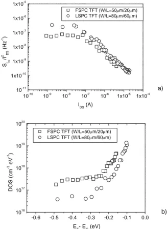
Figure 3 a) Normalized drain current spectra versus drain cur-rent for FSPC and LSPC TFTs, b) DOS into the band gap for the FSPC and the LSPC TFTs versus the position of the Fermi level into the band gap. After [2].
nate and α increases versus the Fermi level into the band-gap following (M-m)/N ratio (see fig. 2), with M-m as the trapping centre number. M and m are associated with trap states around the Fermi level (fixed by the gate voltage).
Validity of these theoretical predictions has been pre-viously experimentally demonstrated [2,7].
The number of trapped carriers into the oxide is strongly controlled by the distribution of interface states. Therefore, considering traps located around the Fermi level, the density of deep states (DOS) into the polysilicon band-gap at the interface can be deduced from the normalized drain current spectral according to (1) and (2) by standing [2]:
( )
( )
D I 2 D 2 F DOS OX GS DOS OX S I kTf WLz 4λ WLzkT m E N V N ≈ ∝ ≈ (4)Plots of the DOS for the FSPC and the LSPC TFTs are re-ported in the figure 3. The lower value of the DOS (one order of magnitude) for LSPC devices suggests a lower number of trapped carriers due to a lower density of deep states associated to dangling bonds close to the
interface. This result is related to a better crystal quality of the active layer because of the laser annealing. Further-more, M-m values were deduced in the strong inversion for
Figure 4Schematic conducting region at GB in circular
grey area.
the two types of devices: M-m~107 (ie M≥107) for FSPC
TFT and M-m~108 (ie M≥108). The higher value for LSPC
structures is related to a higher total density of oxide traps M attributed to a possible contamination of the oxide from the glass substrate and to a lowering of the density of de-fects at the interface during the laser annealing.
These results show the effect of the laser annealing on the 1/f noise level depending on the gate oxide interface quality related to the crystal quality of the layer.
3.2 Current crowding. In this section the noise analysis is supported by the theory of the current crowding (CC) due to structural defects inducing non conducting cavities. CC leads to an overestimation of the measured noise pa-rameter in relation to the quality of the interface and/or of the active layer described as follow.
Trapping carriers at defects induce energy barrier modelled by non conducting cavities. In this case [9]:
eff H α α Ω Ω = (5) with Ω and Ωeff standing for the volume of the full
con-ducting region and of the restricted concon-ducting one respec-tively, and αH the noise parameter in homogeneous
materi-als. In this model a constant noise parameter αH is
consid-ered in the whole semiconductor, but a few cavities do not participate to the conductivity due to high energy barriers. The current density is higher near the non conducting cavi-ties than in homogeneous situation, leading to a higher noise parameter. The number of the non conducting cavi-ties remains constant but their dimension decrease (higher Ωeff) with the gate bias. If we consider a circular restricted
conducting region at grain boundary (see figure 4) then (5) becomes [9]: Grain boundary H Current flow Grain H H H -0.6 -0.5 -0.4 -0.3 -0.2 -0.1 0.0 1016 1017 1018 1019 1020 DOS ( c m -3 eV -1 ) EF- EC (eV) FSPC TFT (W/L=50μm/20μm) LSPC TFT (W/L=80μm/60μm) a) b) 10-10 10-9 10-8 10-7 10-6 1x10⁻⁵ 1x10⁻⁴ 10-11 1x10⁻¹⁰ 1x10⁻⁹ 1x10⁻⁸ 1x10⁻⁷ 1x10⁻⁶ 1x10⁻⁵ FSPC TFT (W/L=50μm/20μm) LSPC TFT (W/L=80μm/60μm) SI DS /I 2 DS (Hz -1 ) IDS (A)
4 Author, Author, and Author: Short title
Copyright line will be provided by the publisher
3 3 20 a H αH π = α (6)
where H is the grain size and a the radius of the restricted conducting contact region at GB.
At low gate voltages (from weak to moderate inversion) energy barriers are maximum, the current flows preferen-tially the lowest barriers in restricted contacts regions and then α>αH. At high gate voltages (from weak to strong
in-version) the energy barriers decrease, the current density becomes uniform and α~αH. Then, for homogeneous
mate-rials αH/α~1 whereas for disordered materials αH/α<<1
and this ratio can be considered as a quality factor of the polycrystalline silicon and thus as an indicator on the reli-ability of the TFTs. Next, CC is experimentally demon-strated.
For TFTs operating in the linear mode, it is commonly admitted that the drain current is strongly controlled by (in-tergranular) energy barriers (EB) accordingly:
( )
(
)
DS 0 GS ox GS B fe0 DS kT C V V V V E exp μ L W I ⎟⎟ − ⎠ ⎞ ⎜⎜ ⎝ ⎛ − ≈ (7)with μfe0 the optimum carrier field effect mobility at high
gate voltages (EB<kT), Cox the gate oxide capacitance per
unit area, L(W) the length(width) of the channel, and V0
the gate voltage defined as the gate voltage corresponding to the minimum of drain current of the transfer characteris-tic IDS=f(VGS). Thus, defining the sheet resistance as
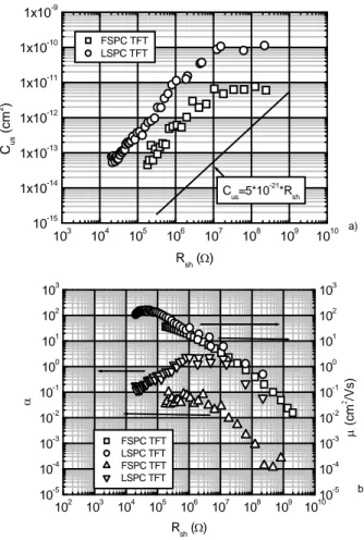
Rsh=(VDS/IDS)(W/L), in this case CC is characterized by
standing 1/f noise in a relative noise level for a unit area [10]: sh DS DS I us WL KR I S f C = 2 = (8) where K=αqμ (q elementary charge) with a value of 5×10-21cm2/Ω (=K
Au) obtained for gold resistor, and that
can be used as a figure of merit [10]. Plots of Cus versus
Rsh reported in the figure 5 a) for the two types of TFTs
show that K≥KAu and indicate CC on a microscopic scale.
Furthermore, we report in the figure 5 b) the plots of α and μfe versus Rsh. α values were previously deduced in
functi-on of VGS according to a protocol described in ref [7], and
μ is calculated from the transconductance gm=dIDS/dVGS
measured in the linear mode. The reported values of α are higher than in crystalline silicon (c-Si) MOS transistors (in ref [7] 10-6<α<10-2), because of a higher defect density in
polysilicon TFTs corresponding to Ω/Ωeff>1 in (5). In
addi-tion, plots of the figure 5 a) show that K value is higher for LSPC TFTs than in FSPC TFTs. This is both explained by higher noise parameter and field effect mobility in LSPC devices (figure 5 b). According to (6), higher values of α for LSPC TFTs are related to a higher V/a ratio explained by a higher grain size and/or a lower defect density at the
grain boundary, also confirmed by a higher field effect mobility in the laser annealed polysilicon layer.
These results are consistent with those previously ob-served by analysis of 1/f noise following the theory of T/D
Figure 5 a) Cus versus Rsh for FSPC and LSPC TFTs, b)
Field effect mobility and noise parameter versus sheet re-sistance for FSPC and LSPC TFTs.
processes of carriers at oxide traps close to the interface. Therefore, analysis of the 1/f noise following the theory of the CC is also a good diagnostic tool to qualify the active layer.
4 Concluding remarks Laser annealing effect of the polysilicon active layer is pointed out on the low frequency noise level in TFTs. Measurements show that noise level is strongly dependent on the gate oxide interface and polysilicon active layer qualities. Analysis shows that noise level can be reduced by improvement of the active layer crystal quality. Therefore, 1/f noise measurement is a good criterion of quality on the microscopic scale of the polysilicon layer, and thus it is a hyperfine diagnostic tool to qualify and to improve TFT technology.
a) b) 102 103 104 105 106 107 108 109 1010 10-5 10-4 10-3 10-2 10-1 100 101 102 103 10-5 10-4 10-3 10-2 10-1 100 101 102 103 μ (c m 2 /V s) α Rsh (Ω) FSPC TFT LSPC TFT FSPC TFT LSPC TFT 103 104 105 106 107 108 109 1010 10-15 1x10-14 1x10-13 1x10-12 1x10-11 1x10⁻¹⁰ 1x10⁻⁹ C us=5*10 -21 *R sh Cus (cm 2 ) Rsh (Ω) FSPC TFT LSPC TFT
pss-Header will be provided by the publisher 5
Acknowledgements The authors acknowledge R. Rogel and J. F. Michaud from the IETR for elaboration of polysilicon layers and TFT processing.
References
[1] M. Aoki, T. Hashimoto, T. Yamanaka, T. Nagano, Jap. J. Appl. Phys. 35, 838 (1196)
[2] L. Pichon, A. Boukhenoufa, C. Cordier, B. Cretu, J. Appl. Phys. 100, 54504 (2006)
[3] C.A. Dimitriadis, G. Kamarinos, J. Brini, IEEE Elect. Dev. Lett. 22, 381 (2001)
[4] A. Mercha, L. Pichon, R. Carin, K. Mourgues, O. Bonnaud, Thin Solid Films 383, 303 (2001)
[5] L.Pichon, K. Mourgues, F.Raoult, T. Mohammed-Brahim, K. Kis-Sion, D. Briand, O. Bonnaud, Semicond. Sci. Tech-nol. 16, 918 (2001)
[6] J. F. Michaud, Ph.D Dissertation, University of Rennes 1, France (2004)
[7] A.Boukhenoufa, L.Pichon, C.Cordier, B.Cretu, L.Ding, R.Carin, J. F. Michaud, T. Mohammed-Brahim, Proceed-ings of: Noise and Fluctuations: 18th International Confer-ence on Noise and Fluctuations-ICNF 2005, edited by T. Gonzalez,J. Mateos, and D. Pardo, pp 319-322
[8] F. N. Hooge, Physica B 336, 236 (2003)
[9] A. Mercha, L. K. J. Vandamme, L. Pichon, R. Carin, J. Appl. Phys. 90(8), 4019 (2001)
[10] L.K.J.Vandamme, H.J.Casier, Proceedings of 34th ESSDERC, editors R.P.Mertens and C.L.Claeys, pp 365-368
![Figure 2 Theoretical variations of noise parameter versus the Fermi level position into the bandgap (after [7])](https://thumb-eu.123doks.com/thumbv2/123doknet/11587488.298475/3.892.80.426.168.687/figure-theoretical-variations-parameter-versus-fermi-position-bandgap.webp)