HAL Id: tel-02112135
https://pastel.archives-ouvertes.fr/tel-02112135
Submitted on 26 Apr 2019HAL is a multi-disciplinary open access
archive for the deposit and dissemination of sci-entific research documents, whether they are pub-lished or not. The documents may come from teaching and research institutions in France or abroad, or from public or private research centers.
L’archive ouverte pluridisciplinaire HAL, est destinée au dépôt et à la diffusion de documents scientifiques de niveau recherche, publiés ou non, émanant des établissements d’enseignement et de recherche français ou étrangers, des laboratoires publics ou privés.
high-speed communications
Heming Huang
To cite this version:
Heming Huang. Optical nonlinearities in quantum dot lasers for high-speed communications. Optics / Photonic. Télécom ParisTech, 2017. English. �NNT : 2017ENST0012�. �tel-02112135�
Télécom ParisTech
école de l’Institut Mines Télécom – membre de ParisTech
46, rue Barrault – 75634 Paris Cedex 13 – Tél. + 33 (0)1 45 81 77 77 – www.telecom-paristech.fr
2017-ENST-0012
EDITE ED 130
présentée et soutenue publiquement par
Heming Huang
le 13 mars 2017Optical nonlinearities in quantum dot lasers for high-speed
communications
Doctorat ParisTech
T H È S E
pour obtenir le grade de docteur délivré par
Télécom ParisTech
Spécialité “ Communications & Electronique ”
Directeur de thèse : Frédéric GRILLOT Co-encadrement de la thèse : Didier ERASME
T
H
È
S
E
JuryM. Christophe LABBE, École Nationale Supérieure d'Ingénieurs de Caen Rapporteur M. Ammar SHARAIHA, École Nationale d'Ingénieurs de Brest Rapporteur M. Dieter BIMBERG, Technische Universität Berlin Examinateur M. Olivier DURAND, Institut National des Sciences Appliquées de Rennes Examinateur M. Fan-Yi LIN, National Tsing Hua University Examinateur M. Philip POOLE, National Research Council Canada Examinateur M. Frédéric GRILLOT, Télécom ParisTech Directeur de thèse M. Didier ERASME, Télécom ParisTech Co-directeur de thèse
1
Acknowledgements
First of all, I would like to express my sincere gratitude and appreciation to my supervisors, Prof. Frédéric Grillot and Prof. Didier Erasme, for their excellent patient guidance and vive support all along my Ph.D. study. I have learned a lot from their constant knowledge, professional approach, and rigorous attitude towards scientific research. I thank them for offering me international exchanges in different countries with multiple leading groups in the field, as well as for supporting me on various international conferences that help me to catch the most recent research topics and technology advances in industrial area. Working with them is a great experience which will be without doubt invaluable beneficial to my future career.
I would like to thank Prof. Dieter Bimberg from Technische Universität Berlin, Germany, and Dr. Philip Poole from National Research Center, Canada, Prof. Fan-Yi Lin from National Tsing Hua University, Taiwan and Dr. Jean-Guy Provost from III-V Lab, France for providing me all the experimental matters that made this work possible. Their high-quality laser samples and unique platform allowed me to achieve a rich variety of results sustaining the comprehension of underlying physics. I would thank equally Dr. Kathy Lüdge from Technische Universität Berlin, Germany, Dr. Paolo Bardella, Dr. Mariangela Gioannini, and Prof. Ivo Montrosset from Politecnico di Torino, Italy for hosting me in their renowned groups. Their thorough and enlightening understanding in optoelectronics granted me important guidance on my research work.
A special thank for Dr. Kevin Schires from Telecom ParisTech, France and Dr. Cheng Wang from ShanghaiTech University, China. They aid and support me tremendously to build up the experimental abilities and theoretical background in my Ph.D. work.
I would also thank Dejan Arsenijević, Tagir Sadeev, Holger Schmeckebier, Christoph Redlich from Technische Universität Berlin, Germany, Lu-Chih Lin, Chih-Ying Chen from National Tsing Hua University, Taiwan, Dr. Mohamed Chaibi from Télécom ParisTech, France and Dr. Ravi Raghunathan from Virginia Tech, USA for the collaborations which pulled off significant results.
2
I appreciate all our collaborators Prof. Yves Jaouen, Dr. Renaud Gabet, Dr. Louise Jumpertz, Damien Maraval, Dr. Xin You, Dr. Mengdi Song from Télécom ParisTech, France, Prof. Marek Osiński from University of New Mexico, USA, Wei Wei, Prof. Lilin Yi from Shanghai Jiaotong University for meaningful scientific discussions.
I would like to thank all the professors, all my colleagues and all the friends in GTO group, Télécom ParisTech who aid me in work and in life.
I acknowledge the Institut Mines-Telecom for supporting my Ph.D. work via Futur & Rupture funding.
Last but not least, I am very grateful to my wife and my parents for their persistent support and encouragement.
3
Table of content
Acknowledgements ...1 Table of content ...3 List of acronyms ...7 List of figures ...9 List of tables ... 19 Chapter I. Introduction ... 21 I. Optical networks ... 21II. Quantum dot lasers ... 25
1. Development history ... 25
2. GaAs-based QD lasers ... 27
3. InP-based QD lasers ... 30
III. Motivations of the dissertation ... 33
1. Narrow linewidth QD lasers for coherent communications... 35
2. QD lasers-based optical wavelength converters ... 35
3. Feedback resistant QD lasers ... 37
IV. Organization of the dissertation ... 39
Chapter II. Fundamentals of quantum dot lasers ... 41
I. Electronic structure ... 41
II. Carrier dynamics ... 44
1. Carrier capture ... 45
2. Carrier relaxation ... 45
III. Gain broadening mechanisms ... 46
IV. Gain dynamics ... 49
1. Linewidth broadening factor ... 49
2. Stability analysis, relaxation oscillations and damping ... 52
3. Nonlinear carrier dynamics ... 55
4
5. Optical spectral linewidth ... 59
V. Summary ... 60
Chapter III. Advanced characterizations of quantum dot lasers ... 61
I. Investigated QD laser devices ... 61
1. InAs/GaAs QD lasers ... 61
2. InAs/InP QD lasers ... 67
II. Linewidth broadening factor ... 71
1. Below-threshold measurements ... 72
2. Above-threshold measurements ... 76
III. Optical spectral linewidth ... 86
1. Self-heterodyne method ... 86
1. Experimental results ... 87
2. Spectral linewidth reduction under external control ... 93
IV. Summary ... 94
Chapter IV Nonlinear conversion in optically-injected QD lasers ... 97
I. Introduction ... 97
II. Four-Wave Mixing... 99
1. Phase conjugation generation ... 99
2. NDFWM in semiconductor gain medium ... 101
3. Extraction of the third-order nonlinear susceptibility ... 106
4. Optical injection-locking ... 108
III. Experimental investigation of four-wave mixing in injection-locked QD lasers ... 112
1. Experimental setup ... 112
2. Static conversion in InAs/InP FP QD lasers ... 113
2.2. Influence of the pump wavelength ... 120
3. Nonlinear conversion with InAs/GaAs QD lasers ... 127
4. Summary ... 134
IV. Dynamic conversion ... 137
1. Experimental setup ... 137
5
3. Conversion performance characterization ... 139
V. Conclusions ... 140
Chapter V. Delay dynamics in quantum dot Lasers ... 141
I. Introduction ... 141
1. Principle of optical feedback ... 141
2. Fundamentals of optical feedback ... 142
II. Theoretical analysis of external optical feedback ... 145
1. Lang & Kobayashi equations ... 145
2. Light-current characteristics with optical feedback ... 147
3. Phase conditions ... 149
4. Critical level boundary ... 152
5. Low-frequency fluctuations ... 156
6. Regular pulse package ... 158
III. Experimental analysis of the long-delay feedback dynamics of QD lasers... 160
1. Experimental setup ... 160
2. Identification of the feedback regimes ... 161
3. InAs/GaAs QD FP lasers ... 164
4. GS chaotic dynamics ... 168
IV. Experimental analysis of the short-delay dynamics of QD lasers ... 169
1. Experimental Setup ... 169
2. GS vs. ES feedback dynamics ... 170
2.3. Analysis of the excited periodic oscillations ... 174
2.4. Self-pulsating dynamics ... 177
V. Summary ... 182
Chapter VI. Conclusions and perspectives ... 183
Appendix 1: Synthèse en français ... 189
I. Introduction ... 189
II. Conversion nonlinéaire en longueur d'onde dans les lasers QD ... 190
1. Principe du mélange à quatre-ondes ... 190
6
3. Configurations expérimentales ... 194
4. Conversion statique... 195
5. Extraction de la susceptibilité nonlinéaire de troisième-ordre 𝝌(𝟑) ... 198
6. Conversion dynamique dans les lasers QD ... 199
7. Résumé ... 201
III. Dynamiques nonlinéaires des lasers QD sous retour optique externe ... 202
1. Principe de la rétroaction optique ... 202
2. Rétroaction optique dans les lasers QD ... 204
3. Configuration expérimentale ... 206
4. Dynamiques nonlinéaire des lasers QD rétroactionnés dans les cavités longues 208 5. Dynamiques nonlinéaire des lasers QD rétroactionnés dans les cavités courtes . 211 6. Résumé ... 213
IV. Réduction de la Largeur de raie dans les lasers QD ... 214
1. Largeur de optique des lasers QD ... 214
2. Configuration expérimentale ... 214
3. Réduction de la largeur de raie par rétroaction optique ... 216
4. Résumé ... 217
Appendix 2: List of Publications ... 219
Journal Papers ... 219
Conference Papers ... 219
7
List of acronyms
Abbreviation Stand for
AOM Acousto-Optical Modulator
ASE Amplified Spontaneous Emission
CDP Carrier Density Pulsation
CE Conversion Efficiency
CH Carrier Heating
DFB Distributed FeedBack laser
DOS Density Of States
DWELL Dot-in-WELL structure
ES Excited-State
ESA Electrical Spectrum Analyzer
FM/AM Frequency Modulation / Amplitude Modulation
FP Fabry-Perot
FSR Free Spectral Range
FWM Four-Wave Mixing
GS Ground-State
LEF Linewidth Enhancement Factor
LIV Light-current-Voltage
LI Light-current
NCE Normalized Conversion Efficiency
NDFWM NonDegenerate Four-Wave Mixing
OIL Optical Injection Locking
OSA Optical Spectrum Analyzer
OSNR Optical Signal-to-Noise Ratio
PD PhotoDiode
QW Quantum Well
QWire Quantum Wire
QD Quantum Dot
RS Reservoir State
RWG Ridge WaveGuide
SCH Separate Confinement Heterostructure
8
TL Tunable Laser
WDM Wavelength Division Multiplexing
WL Wetting Layer
WPE Wall-Plug Efficiency
XGM cross-Gain Modulation
9
List of figures
Figure 1.1. IP traffic compound annual growth rate (CAGR) in exabyte per month, after [2]. 21 Figure 1.2. Schematic of the current optical network infrastructure. ... 22 Figure 1.3. Evolution of the density of states (DOS) for (a) bulk material, (b) quantum well (QW), (c) quantum wire (QWire) and (d) quantum dots (QD), after [37]. ... 26 Figure 1.4. Chronological progress of the threshold current density for semiconductor lasers. The last data set to the right shows the evolution of the threshold current density per layer for GaAs-based QD lasers as compare to bulk and QW laser structures, after [38]. ... 27 Figure 1.5. Plan-view transmission electron microscopy image of a single QD layer with nanostructures formed by (a) 2.5 monolayers InAs deposition followed by GaAs overgrowth and (b) 2.5 monolayers InAs deposition followed by overgrowth with a 5-nm-thick In0.15Ga0.85As
layer prior to GaAs deposition, after [49]. ... 28 Figure 1.6. Light-Current-Voltage (LIV) characteristics of an InAs/GaAs QD laser grown by hetero-epitaxy on silicon, after [22]. ... 30 Figure 1.7. The formation of InAs nanostructures on InP (001) as a function of trimethylindium (TMIn) flow and growth temperature, after [75]. ... 31 Figure 1.8. Cross-section scanning-electron-microscopy (X-SEM) image of an InAs/InP QDash laser grown by MBE at the National Research Council (NRC) Canada (courtesy of Dr. Philip Poole). ... 31 Figure 1.9. Chronological progress of the threshold current density per layer for InAs/InP QD and QDash lasers, after [77]. ... 32 Figure 2.1. (a) 3-D schematic of a QD p-i-n-doped semiconductor laser diode. The yellow region is the undoped active region, and the black triangles represent the dots. (b) Cross-section of the schematic in (a), showing the material composition and thickness of each layer. (c) Energy band alignment of the heterostructure along the x-axis, after [142]. ... 42 Figure 2.2. Schematic of a QD laser electronic structure with electrons and holes, after [146]. ... 43 Figure 2.3. Illustration of the carrier capture and relaxation processes: a) multi-phonon
10
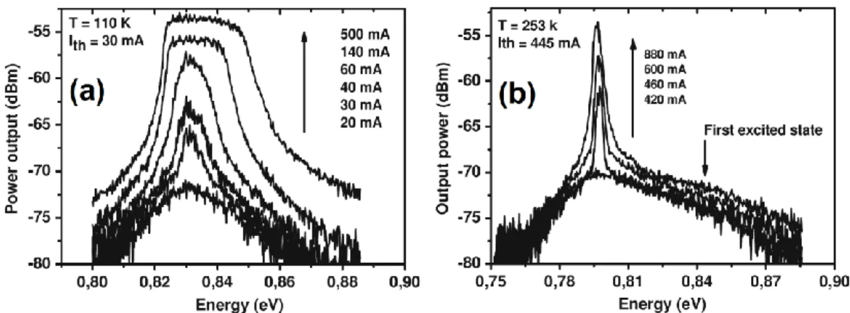
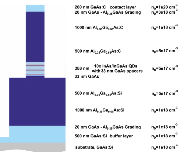
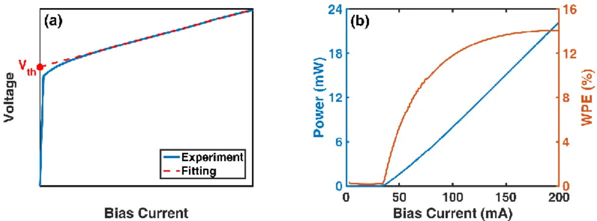
processes under low excitation density, b) single Auger process, and c) sequential Auger processes under high injection current density, after [152]. ... 44 Figure 2.4. The capture rate as a function of the carrier density, after [159]. ... 45 Figure 2.5. Representation of the inhomogeneous broadening illustrating dots with different sizes, and leading to an energy state distribution, after [168]. ... 47 Figure 2.6. Photoluminescence spectrum as a function of temperature from a single InAs/GaAs dot, after [177]. ... 48 Figure 2.7. Lasing and electroluminescence spectra under pulsed injection mode for different bias level at two different temperatures: (a) 110K and (b) 253 K, after [178]. ... 48 Figure 2.8. (a) Schematic of gain g and refractive index n profiles variation with the carrier density changes for QW and symmetric QD ensemble, after [194]; (b) gain (g) and refractive index (n) profiles versus αH-factor in symmetric QD ensemble, which is compared to
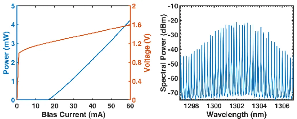
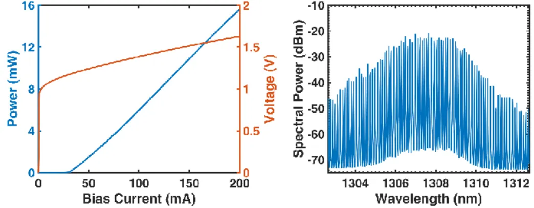
asymmetric QD ensemble, after [43]. ... 51 Figure 2.9. Modulation response of a semiconductor laser. The blue arrow indicates the increase of the bias current, after [192]. ... 55 Figure 2.10. Representation of the carrier energy distributions 𝜂(𝐸) after propagation of an optical pulse within the semiconductor medium pumped in the gain regime, after [142]. ... 56 Figure 2.11. Gain recovery dynamics for (a) a QD-SOA and (b) a QW-SOA as a function of different pump currents. The pump pulse duration is (a) 12 ps and (b) ~20 ps. The input pump pulse energy: (a) ~40 fJ and (b) ~300 fJ, after [204]. ... 57 Figure 2.12. The evolution of 𝑛𝑠𝑝(1 + 𝛼𝐻2) as a function of modal gain in bulk, single QW (SQW), multi-QW (MQW) material as compared to a six-layer InAs/GaAs QD DFB laser (6QD), after [217], [218]. ... 60 Figure 3.1. Epi-layer structure of the InAs/GaAs QD lasers (courtesy of Prof. Dieter Bimberg). ... 62 Figure 3.2. InAs/GaAs QD FP laser bar with 1-mm long lasers. ... 62 Figure 3.3. (a) Typical laser VI curve and extraction method for 𝑅𝑠 and 𝑉𝑡ℎ values; (b) output power and WPE as a function of bias current for QD laser GaFP4. ... 64 Figure 3.4. LIV curves (left) and optical spectrum (right) of the InAs/GaAs QD laser GaFP1. . 65 Figure 3.5. LIV curves (left) and optical spectrum (right) of the InAs/GaAs QD laser GaFP2. . 65
11
Figure 3.6. LIV curves (left) and optical spectrum (right) of the InAs/GaAs QD laser GaFP3. . 65
Figure 3.7. LIV curves (left) and optical spectrum (right) of the InAs/GaAs QD laser GaFP4. . 66
Figure 3.8. LIV curves (left) and optical spectrum (right) of the InAs/GaAs QD laser GaFP5. . 66
Figure 3.9. PL spectrum at 8 K from an InAs/GaAs QD sample grown by the same technology than the InAs/GaAs QD lasers studied in this thesis, after [223]. The GS-ES separation is 65 meV [174]. ... 67
Figure 3.10. (a) Schematic diagram of the InAs QD structure, after [38]; (b) An atomic-force microscopy image of one QD layer (1 µm × 1 µm) (courtesy of Dr. Philip Poole). ... 67
Figure 3.11. (a) InAs/InP QD laser PDFB2 (Scale: 500 µm); (b) cross-section view of the DFB structure. ... 68
Figure 3.12. PL spectrum from a five-layer InAs/InP QD sample grown by the same CBE technology, after [53]. ... 69
Figure 3.13. Output power and WPE as a function of the bias current in QD laser PFP1. ... 69
Figure 3.14. LIV curves (left) and optical spectrum (right) of InAs/InP QD laser PFP1. ... 70
Figure 3.15. LIV curves (left) and optical spectrum (right) of InAs/InP QD laser PDFB1. ... 70
Figure 3.16. LIV curves (left) and optical spectrum (right) of the InAs/InP QD laser PDFB2. .. 71
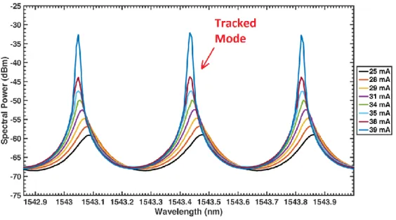
Figure 3.17. Sub-threshold optical spectra of QD laser PFP1 for different bias currents. ... 73
Figure 3.18. Net modal gain spectra of QD laser PFP1 for various bias current conditions. ... 74
Figure 3.19. The net gain and refractive index variations of the mode around 1543.3 nm (see in Figure 3.17) in QD laser PFP1. Red solid lines: linear fitting below threshold; Green solid lines: linear fitting above threshold. ... 74
Figure 3.20. The measured αH-factor spectral dependence for QD laser PFP1. ... 75
Figure 3.21. The measured αH-factor for the GS QD laser GaFP1 and ES QD laser GaFP2. ... 76
Figure 3.22. Free-space experimental setup used for the FWM analysis. TL: tunable laser; LD: QD laser diode; FR: Faraday rotator; HW: half-wave plate; PBS: polarizing beam splitter; PD: photodiode; SA: electric spectrum analyzer; VA: variable attenuator; AOM: acousto-optic modulator; B: beam block; FC: 50/50 fiber coupler, after [232]. ... 78
Figure 3.23. Measured (a) normalized regenerated signals intensity and (b) normalized beating intensity of the 100 MHz shifted probe and wave mixing QD laser PDFB1 under FWM at 3×Ith (red dots). Blue solid curves represent the fitting calculated from the analytical model. ... 79
12
Figure 3.24. The retrieved αH-factor of QD laser PDFB1 as a function of the bias current. .... 80
Figure 3.25. Schematic of the experimental setup used for FM/AM measurements, after [227]. ... 81 Figure 3.26. Transfer function of the MZ interferometer [37]. ... 82 Figure 3.27. (a) The measured 2𝛽/𝑚 ratio of QD laser PFP1 at 298K under 2 × 𝐼𝑡ℎ bias, the red solid line gives the αH-factor value ~6; (b) the measured αH-factor as a function of the bias
current. ... 84 Figure 3.28. Numerical simulation of carrier variations at 𝐼 = 1.2 × 𝐼𝑡ℎ. The carrier variations are normalized to the value 𝛿𝑁𝐺𝑆 of 0.01 GHz at lasing threshold 𝐼𝑡ℎ, after [37]. ... 85 Figure 3.29. The measured αH-factor of QD laser PDFB2. The red line is the fitting from Eq. 2.34.
... 86 Figure 3.30. Self-heterodyne experimental setup used for the optical linewidth measurement. ... 87 Figure 3.31. RF spectrum of QD DFB laser PDFB2 recorded at 95 mA (298K). ... 88 Figure 3.32. Normalized RF spectrum from Figure 3.31 (blue dots) and the corresponding Voigt fitted spectrum (red solid line). ... 89 Figure 3.33. The measured optical spectral linewidth as a function of the total output power of QD laser PDFB2... 90 Figure 3.34. The measured optical spectral linewidth as a function of the total output power for QD laser PDFB1. ... 91 Figure 3.35. The measured optical spectral linewidth as a function of the total output power for a packaged QW DFB laser from Nokia. ... 92 Figure 3.36. Feedback arm inserted at the upstream of the linewidth measurement setup shown in Figure 3.30. ... 93 Figure 3.37. Measured spectral optical linewidth of QD laser PDFB1 under external optical feedback. The blue triangles correspond to five different measurements done in sequence; the black dotted line represents the spectral linewidth of the free-running laser. ... 94 Figure 4.1. Illustration of the NDFWM process, the interaction of fields 𝐸1 and 𝐸2 at the frequencies of 𝜔1and 𝜔2 leads to the generation of fields 𝐸3and 𝐸4 at 𝜔3and 𝜔4. ... 97 Figure 4.2. Schematic illustration of the NDFWM in a semiconductor gain medium. ... 101
13
Figure 4.3. The contributions of the CDP, CH and SHB mechanisms to the nonlinear conversion efficiency in a QD SOA device, after [118]. ... 102 Figure 4.4. Directions of 𝜒(3) of CDP and SHB for bulk, QW and QD, after [116]. ... 104 Figure 4.5. Comparison of the measured CE between a bulk and a QD SOA, after [102]. .... 105 Figure 4.6. Scheme illustrating the optical injection-locking. ... 109 Figure 4.7. Optical spectra of the free-running FP laser (blue) and of the injection-locked laser (red). ... 110 Figure 4.8. Illustration of the injection-locking boundaries in terms of injection detuning and injection strength, after [276]. SL: stable locking; NL: nonlinear dynamics area. ... 112 Figure 4.9. Experimental setup for NDFWM investigation, the pump signal originates from tunable laser TL1, whose beam is seeded into the QD laser and injection-locked it. ... 112 Figure 4.10. Measured CE (a), NCE (b) and OSNR (c) of FWM in the QD laser PFP1 as a function of the pump-probe frequency detuning. ... 115 Figure 4.11. Intensity mode profile in the x and y directions (left) and corresponding distribution in the waveguide cross-section (right). ... 116 Figure 4.12. The normalized third-order nonlinear susceptibility 𝜒(3)/𝑔0 as a function of the pump-probe frequency detuning. ... 117 Figure 4.13. Numerical simulations showing the output power as a function of the injection detuning for an injection-locked QD FP laser. Green: 𝑃𝑜𝑢𝑡 from the same facet (left); Red: 𝑃𝑜𝑢𝑡 of the slave laser only from the left facet; Pink: 𝑃𝑜𝑢𝑡 from the right facet of the laser; Dashed line: reflected pump alone. ... 118 Figure 4.14. Experimental results illustrating the impact the injection ratio on the output power measured at the two facets of a QD FP laser. The pump is injected from the left facet. ... 119 Figure 4.15 NDFWM spectra of the QD FP laser measured in reflection and transmission configurations for a pump-probe frequency detuning of 340 GHz (down-conversion). ... 119 Figure 4.16. Measured CE versus frequency detuning for different pump wavelengths for (a) down-conversion and (b) up-conversion. The red, blue and green curves represent the results obtained for 1538, 1543 and 1548 nm respectively. ... 120 Figure 4.17. The normalized 𝜒(3)/𝑔0 as a function of the pump-probe frequency detuning and
14
for different injected pump wavelengths. The red, green and blue colors represent the results obtained when the pump mode is at 1538, 1543 and 1548 nm, respectively. ... 121 Figure 4.18. The measured CE as a function of the pump-probe frequency detuning for down-conversion (a) and up-down-conversion (b) for the two TL1 under study. ... 122 Figure 4.19. 𝜒(3)/𝑔0 as a function of the pump-probe frequency detuning for the two TL1 under study. ... 122 Figure 4.20 The LIV characteristics of the (a) QD FP laser PFP2 and (c) QDash FP laser PFP3; the optical spectrum of (b) PFP2 and (d) PFP3 is measured at 2.5 × 𝐼𝑡ℎ. ... 123 Figure 4.21 (a) Net gain and (b) αH-factor spectral dependence for both QD FP laser PFP2 and
QDash FP laser PFP3. ... 124 Figure 4.22 NCE of QD PFP2 and QDash PFP3 measured using the same setup and experimental conditions as for PFP1. The inset represents the corresponding OSNR. ... 125 Figure 4.23. The αH-factor spectral dependence for QD lasers GaFP3 and GaFP4 measured by
the ASE method. The gain peaks are around 1309 nm for both lasers. ... 128 Figure 4.24 The measured CE as a function of the pump-probe frequency detuning for QD lasers (a) GaFP3 and (b) GaFP4 under 2.4 × 𝐼𝑡ℎ and 1 dB pump injection strength. Filled (resp. empty) triangles represent up (resp. down) conversion. The figures in inset show the corresponding OSNR of QD lasers GaFP3 and GaFP4. ... 129 Figure 4.25 (a) CE as a function of the pump-probe wavelength detuning; (b) CE within an SOA made with the same material, after [112]. ... 130 Figure 4.26. (a) CE and (b) OSNR in QD laser GAFP5 (2 mm) and QD laser GAFP3 (1.5 mm).131 Figure 4.27. (a) CE and (b) OSNR in the 1.5 mm × 2 µm QD GaFP3 laser at two different bias currents... 131 Figure 4.28. Schematic of injection-locking map, red dot marks the same injection conditions for the three pump wavelengths used in section III.2.2, and the blue arrows indicate the local tuning of the injection conditions with respect to the stable-locking (SL) area. ... 132 Figure 4.29. (a) CE and (b) OSNR in QD laser GaFP3 at two different pump injection ratios; (c) CE and (d) OSNR in GaFP3 at two different pump master-slave injection detunings. ... 133 Figure 4.30. Pump optical spectra at different injection frequency detunings. ... 134 Figure 4.31. Schematic of the experimental setup dedicated for dynamical conversion. MZM:
15
Mach-Zehnder modulator; PPG: pulse pattern generator; TBPF: thin band-pass filter; SMF: single mode fiber; EDFA: Erbium-doped fiber amplifier; Osc.: oscilloscope; BERT: bit error rate test. ... 138 Figure 4.32. Back-to-back eye diagram of the converted signal with a modulation of 2.5 Gbps PRBS sequence of length of 27-1 by using (a) Yenista T100 (1550 nm) and (b) Tunics as the TL2.
... 138 Figure 4.33. BER curves as a function of the receiving power by the detector for the probe before injection, the converted signal on back-to-back (Conv.) and after the transmission within 25 km SMF coil. The horizontal dotted black line corresponds to the conventional error-free boundary (BER = 10-9). ... 139
Figure 5.1. Schematic representing a semiconductor laser subjected to conventional optical feedback (COF). ... 141 Figure 5.2. Feedback regimes in a semiconductor DFB laser (center), after Ref. [304]. The optical spectra on both sides illustrate the laser dynamics under optical feedback, after [323]. ... 143 Figure 5.3. (a) LI curves of a QD FP laser under free-running operation (black) and for three different amounts of feedback (𝑟𝑒𝑥𝑡 = 1.7%, 3.4% and 6.7%); (b) Extracted threshold current 𝐼𝑡ℎ from (a) as a function of 𝑟𝑒𝑥𝑡, the red triangle is the free-running value (𝑟𝑒𝑥𝑡 = 0). ... 148 Figure 5.4. Interaction between the ECM Mi and the laser cavity modes Nj, after [303]. .... 148
Figure 5.5. Hysteresis effect in the LI a QD FP laser operating under optical feedback (rext=6.7%)
while increasing and decreasing the bias current. ... 148 Figure 5.6. Solutions of Eq. 5.18 in the (𝐶,𝜑0) space. The roman numbers represent the number of solutions, after [294]. ... 149 Figure 5.7. Steady-state solutions with respect to parameter 𝐶 . Solid and dashed lines are obtained for 𝐶 = 0.76 and 𝐶 = 9.50, respectively. The black circle corresponds to the single solution for 𝐶 < 1 and white circles represent the various solutions for 𝐶 > 1, after [294]. . 150 Figure 5.8. Carrier density Δ𝑁 variation versus the phase difference Δ𝜔𝜏𝑒𝑥𝑡. Crossing points between solid and dashed sine waves give the locations of the modes. The red dot is the free-running mode, while black dots/circles correspond to ECM and antimodes respectively [294]. ... 151
16
Figure 5.9. Optical spectral linewidth as a function of the feedback strength. The markers represent different feedback phase conditions, after [330]. ... 152 Figure 5.10. The critical feedback level 𝑟𝑐𝑟𝑖𝑡 as a function of the external round-trip time 𝜏𝑒𝑥𝑡 (solid line). The dashed line marks 𝐶 = 1, and the vertical line indicates is 𝑓𝑅𝑂× 𝜏𝑒𝑥𝑡 = 1, after [305]. ... 153 Figure 5.11. Sub-boundaries of regime IV as a function of the external cavity length Lext and
feedback strength rext. Fixed: stable state, P1, P2: periodic oscillations, QP: quasi-periodic
oscillations, after [294]. ... 153 Figure 5.12. Excited periodic oscillation frequencies as a function of 𝐿𝑒𝑥𝑡 (black dots), the horizontal line is the free-running ROF (𝑟𝑒𝑥𝑡 = 0), after [335]. ... 156 Figure 5.13. Mapping of the LFF dynamic as a function of the injection current and optical feedback strength. The LFF regime is depicted in light gray. In the dark-gray region stable emission and LFF dynamic coexist. In the undashed region LFF and fully developed coherence collapse coexist, after [339]. ... 157 Figure 5.14. (a) Trajectory of the modes in the (Δ𝑁, Δ𝜔𝜏𝑒𝑥𝑡) plane; (b) Corresponding LFF waveform, after [336]. ... 158 Figure 5.15. The RF spectrum and the corresponding temporal waveform of a semiconductor laser operating under the RPP regime, after [340]. ... 158 Figure 5.16. Trajectory of the modes in the phase domain illustrating the RPP dynamic and the corresponding temporal waveform. ... 159 Figure 5.17. Experimental setup used for the long-delay feedback dynamics. ... 161 Figure 5.18. The optical (a) and RF (b) spectra of QD DFB laser PDFB1 under external feedback with 𝑟𝑒𝑥𝑡 ranging from 0 to 1%. The vertical lines in red allow to distinguish the different feedback regimes. Green dashed lines correspond to the measured operation points of optical ((c), (e), (g), (i)) and RF spectra ((d), (f), (h), (j)). ... 162 Figure 5.19. Optical and spectral mappings of QD DFB laser PDFB1 under external optical feedback at different bias conditions of 1.5× ((a), (b)), 2× ((c), (d)) and 3×𝐼𝑡ℎ ((e), (f)). ... 163 Figure 5.20. The critical feedback level 𝑟𝑐𝑟𝑖𝑡 as a function of the normalized bias level 𝐼/𝐼𝑡ℎ. ... 164 Figure 5.21. (a) Optical and (b) RF spectra of the GS QD laser GaFP1 measured at 3 × 𝐼𝑡ℎ without
17
feedback (𝑟𝑒𝑥𝑡 = 0) and for the maximal feedback strength. ... 165 Figure 5.22. Optical (left) and RF (right) spectral mappings for ES QD laser GaFP2 at (a-b) 1.5 × 𝐼𝑡ℎ, and (c-d) 2 × 𝐼𝑡ℎ. ... 166 Figure 5.23. ES QD laser GaFP2 at 1.5 × 𝐼𝑡ℎ bias level: (a) optical and (b) RF spectra of the free-running laser, at 0.6% and 4.3% optical feedback; GaFP2 at 2 × 𝐼𝑡ℎ bias level: (c) optical and (d) RF spectra of the free-running laser, at 0.1% and 4.6% optical feedback. ... 167 Figure 5.24. (a) Optical and (b) RF spectral mapping of GS QD laser GaFP3 at 2.5 × 𝐼𝑡ℎ with optical feedback. ... 168 Figure 5.25. Experimental setup used for the short-delay feedback investigation. ... 169 Figure 5.26. LI characteristics of the QD ES laser GaFP2 measured at 293 K. ... 170 Figure 5.27. Optical and RF spectral mappings of GS QD laser GaFP1. The external cavity length is 2 cm long. The bias currents are at 1.5 × ((a) and (b)) and 1.7 × 𝐼𝑡ℎ ((c) and (d)). The green and the orange horizontal solid lines mark the frequencies 𝑓𝑒𝑥𝑡 and 𝑓𝑅𝑂 respectively. ... 171 _Toc473564438Figure 5.28. RF spectral mappings ((a), (c)) and RF spectra under free-running (𝑟𝑒𝑥𝑡=0) and for the maximal optical feedback strength (rext = 76%) ((b), (d)) of GS QD laser GaFP1. The external cavity length is 50 cm long. Bias currents are at 1.5× ((a), (b)) and 1.7 × Ith ((c), (d)). The green and the orange horizontal solid lines mark the frequencies fextand fRO respectively. ... 172 Figure 5.29. RF spectral mappings of ES QD laser GaFP2 biased at 1.5 × 𝐼𝑡ℎ under free-running (𝑟𝑒𝑥𝑡= 0) and for the maximal optical feedback strength (𝑟𝑒𝑥𝑡= 55%) considering 2 and 50 cm long external cavity ((a) and (c)); RF spectra under free-running (𝑟𝑒𝑥𝑡 = 0) and for the maximal optical feedback strength (𝑟𝑒𝑥𝑡= 55%) ((b) and (d)). ... 173 Figure 5.30 Excited periodic oscillation frequency fP as a function of external cavity length for
QD lasers GaFP1 and GaFP2 at 1.5 × 𝐼𝑡ℎ ((a), (c)) and at 2 × 𝐼𝑡ℎ ((b), (d)). The vertical solid lines in orange mark the boundaries between the short- and long-delay feedback regime, and the horizontal one in black gives the ROF 𝑓𝑅𝑂 of the free-running laser. ... 175 Figure 5.31. Boundaries of excited periodic and chaotic oscillations as a function of the external cavity length for QD GS laser GaFP1 and QD ES laser GaFP2 at 1.5× 𝐼𝑡ℎ ((a), (c)) and 1.7 × 𝐼𝑡ℎ ((b), (d)). The vertical solid lines in orange mark the boundaries between short- and long-delay feedback regimes... 176
18
Figure 5.32. (a) Temporal waveform and (b) RF spectrum of QD laser GaFP2 cavity at 1.5 × 𝐼𝑡ℎ under 8.5% optical feedback in 20 cm long external cavity at 1.5 × 𝐼𝑡ℎ. ... 178 Figure 5.33. (a) Temporal waveform and (b) RF spectrum of QD laser GaFP2 under 29% optical feedback in 6 cm long external cavity at 1.5 × 𝐼𝑡ℎ. ... 179 Figure 5.34. (a) RF spectrum and (b) temporal waveforms of QD laser GaFP2 for a phase 𝜑0; (c) RF spectrum and (d) temporal waveform of GaFP2 for a phase of φ0+ 10π/3. ... 180 Figure 5.35. Mapping of the dynamical transitions with respect to the feedback strength 𝑟𝑒𝑥𝑡 and the external cavity length 𝐿𝑒𝑥𝑡 (a) 1.5 × and (b) 1.7 × 𝐼𝑡ℎ. In blue and red, the periodic and chaotic oscillation boundaries; the black contours show the windows of self-pulsations. .. 181 Figure 5.36. Measured self-pulsation frequency for ES QD laser GaFP2 as a function of the external cavity length at two bias currents. ... 181
19
List of tables
Table 3.1. Measured intrinsic parameters of the InAs/GaAs QD FP lasers. ... 63 Table 3.2. Measured intrinsic parameters of the InAs/InP QD FP and DFB lasers. ... 70 Table 3.3. The measured αH-factor (gain peak) for GaAs-based QD FP lasers. ... 76
Table 3.4. Extraction procedure of 𝑛𝑠𝑝(1 + 𝛼𝐻2) for QD DFB laser PDFB2. ... 90 Table 4.1. Summary of the state-of-the-art of the NDFWM achievements in QD SOAs and lasers. QW laser results are included for comparison. ... 106 Table 4.2. Experimental conditions used for testing PFP1. ... 114 Table 4.3. Parameters used in Eq. (4.10). ... 117 Table 4.4. Experimental conditions used in InAs/GaAs QD FP laser GaFP1. ... 127 Table 4.5. Impact of the type of nanostructures on the conversion performance (results from InP-based nanostructures). ... 135 Table 4.6. Impact of the αH-factor on the conversion performance (results from InP-based QD).
... 135 Table 4.7. Impact of the cavity dimensions on the conversion performance (results from GaAs-based nanostructures). ... 136 Table 4.8. Impact of the bias current on the conversion performance (results from GaAs-based nanostructures). ... 136 Table 4.9. Impact of the injection strength on the conversion performance (results from GaAs-based nanostructures). ... 136 Table 4.10. Impact of the injection frequency detuning on the conversion performance (results from GaAs-based nanostructures). ... 137 Table 4.11. Impact of the pump linewidth on the conversion performance (results from InP-based nanostructures). ... 137 Table 5.1. Main differences between the RPP and LFF dynamics. ... 159 Table 5.2. ROFs measured at both bias levels for GS laser GaFP1 and ES laser GaFP2. ... 170
21
Chapter I. Introduction
The introduction sets the context and the motivations of the thesis. First, key-features and current challenges of fiber-optics communication networks are described. Then, a brief history of quantum dot lasers (QD) is recalled as well as their potentials for optical communications. Both GaAs- and InAs-based QD lasers are introduced along with the main breakthroughs. Exploiting the nonlinear properties of QDs is the central point of the thesis. To this end, QD lasers operating with external control are introduced with the view to propose novel integrated photonics solutions either for the realization of all-optical wavelength converters, isolator-free transmitters and low phase noise oscillators. Finally, the overall organization of the manuscript will be detailed at the end of this introduction chapter.
I.
Optical networks
Nowadays, semiconductor lasers contribute fundamentally to modern optical communication networks. Every year, several millions of new semiconductor laser devices are used in communication systems, generating several billion dollars of annual revenue at the component level [1].
Figure 1.1. IP traffic compound annual growth rate (CAGR) in exabyte per month, after [2].
With the exponentially growing telecom market, the annual global IP (Internet Protocol) traffic in the optical network will increase threefold in the next five years with a prediction for
22
2020 of 200 exabytes per month (EB, 1 EB = 1018 GB), as illustrated in Figure 1.1 [2]. In addition,
with the wide spread of smartphones and smart devices, these terminals will occupy two third of the total IP traffic by the end of 2020 [2]. Therefore, faster optical sources are on demand to ensure the cost-effective information transmission, which pushes forward the development of novel semiconductor laser technologies. In fiber telecommunications, the C-band (1530-1565 nm) has been widely exploited. At 1550 nm, the loss of single-mode optical fibers (e.g. SMF G. 652) is as low as 0.2 dB/km that is of first importance for long-haul communications. Indeed, low loss means that the distance between repeaters and erbium fiber doped amplifies (EDFA) is long. A second important parameter of the optical fiber is the chromatic dispersion, which contributes to broaden the pulse light during the propagation. With standard SMF optical fibers, the dispersion is null at 1310 nm, which makes the O-band (1260-1360 nm) very suitable for short distances hence avoiding costly dispersion compensating techniques. In today’s networks, the O-band is typically used for up-streaming the data from the customer premises to the central office. Using the O-band for down-streaming data is also considered but this will be expanded in the future.
23
As illustrated in Figure 1.2, the current topology of optical networks is as follows [3]: 1) The access network connects the individual endpoints to the local exchanges, the
interlinks are usually of a few km;
2) The metro network is usually considered in two parts – area network that links the access network in a city, and regional network that connects to other cities, the interlinks varies from a few tens of km up to 1000 km scale;
3) The core network performs all the necessary routing and also serves as the gateway to neighboring core nodes [4], the interlinks are usually several thousands of km and includes the inter-continental connections, as well as the hyperscale data center interconnections.
In particular, numerous short-reach applications requiring high data throughputs are emerging, not only in access networks, where upgrades of the bit rate of passive FTTx (Fiber To The x endpoint) systems need to be anticipated, but also in data center networks, where huge amounts of information may need to be exchanged between servers, in part triggered by the rise of “Big Data” applications. In addition, due the increase of the data traffic, the energy consumption is also becoming very problematic with the substantial growth of global IP traffic. Therefore, fast and low-cost transmitters with low energy consumption are absolutely required, especially for short-reach communication links such as access and data center optical networks. Typically for a few hundred meters to a few km transmission distances, direct modulation with on-off keying (OOK) remains the simplest optical transmitter and receiver architecture and it is thus preferred from investment cost point of view. However, although the fiber dispersion is not a limiting factor in the O-band, a weak frequency-chirped operation is demanded from the laser sources in particular to avoid signal distortion and cross-talk problems.
However, as the link distance increases (from a few km to 1000 km scale), direct modulation is no longer the most effective way to support the transmission rate and reach [5]. Coherent communications have been introduced to increase the long-haul transmission efficiency, especially in metro and core networks [6]. In order to reduce the noise in the detection part, local oscillators with low phase noise is required [7]. Indeed, although the frequency drift of the transmitter can be minimized, the carrier phase still fluctuates randomly
24
because of the phase noise induced from the lasers. Therefore, local oscillator with narrow spectral linewidth is a crucial requirement for realizing stable heterodyne detection. Commercial QW lasers usually exhibit spectral linewidth of a few MHz, in order to reach kHz-spectral linewidth, continuous efforts have been made to decrease the spontaneous emission rate into the lasing mode or to increase the number of photons stored in the cavity. In the latter, high-Q resonator with Q the quality factor defined as the ratio of the energy stored by a cavity to the power lost can lead to a narrow spectral linewidth [8]–[11]. On this stage, different designs of single-mode devices have been proposed to achieve narrow linewidths in the order of 100 kHz or below, such as external cavity [12], chirped grating [13], and discrete mode DFB lasers [9], [10]. In particular, one recent solution was obtained from a proper modal engineering of a DFB laser in which light is generated in the III-V material and stored in the low-loss silicon material. Fabricated lasers using modal engineering to concentrate light in silicon demonstrate spectral linewidths at least 5 times smaller than any other semiconductor lasers [11].
In addition, advanced modulation formats like pulse amplitude modulation (PAM) and phase-shift keying (PSK) and digital signal processing (DSP) would be needed particularly for datacenter interconnects, also leveraging off previous work done for long-haul transmission. Nevertheless, although recently developed DSPs can reach fast operating speed, it has been proved that the long latency introduced by the electronic processing results in a severe communication bottleneck for short-reach communication links [14]. Therefore, direct detection through direct modulation still provides a simple, low cost and compact solution for short reach communication links without suffering from the electronics [5], [7]. However, direct modulation can make the output light strongly dependent on nonlinear laser characteristics. Up to now, external modulators are well-known and commonly used to overcome these problems by providing a larger bandwidth and lower chirp but external modulation still suffers from a higher cost and power consumption [15]. With direct detection, the modulation bandwidth of the laser is the most important feature that determines the maximum data rate achievable. The best performers to date, edge-emitting lasers have achieved modulation bandwidths up to 55 GHz [16], [17]. For very short reach interconnects up to a few hundred meters, inexpensive vertical-cavity surface-emitting lasers (VCSELs) with
25
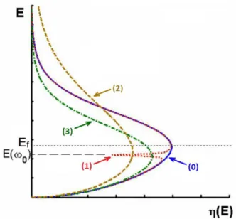
ultra-low threshold are generally used for communications at 10 Gbps within the data centers. Nevertheless, combined with the multimode fiber dispersion, it turns out that VCSELs are not good candidates when the link speed exceeds 20 Gbps. To overcome such a limitation, distributed-feedback (DFB) lasers and single-mode fiber are preferred within the data centers to cover transmissions above 20 Gbps. Numerous results have been published in the literature showing the advantages of various complex DFB structures with higher-power, better temperature performance, and higher speeds [18]–[21]. Although the DFB technology is more expensive, it does provide a higher bandwidth and a relatively narrow spectral linewidth to increase interconnect bandwidth and reach, while maintaining low power consumption and relatively low cost. Overall the development of energy saving quantum-confined devices still constitutes an active field of research [2]. Over the last past years, tremendous efforts have been carried out towards the improvement of semiconductor lasers. All these achievements are actually related to the invention of novel in plane semiconductor materials like those based on QD technology. Such self-organized nanostructures are one of the best practical examples of emerging nanotechnologies. Indeed, due to the atom-like discrete energy levels, QDs exhibit various properties resulting from the three-dimensional confinement of carriers, like a high stability against temperature variation and a low-threshold lasing operation, which are in favor for the reduction of the energy consumptions. Very recently, it was also proved that QDs have a high potential to overcome the inherent problems related to standard diode lasers integrated on silicon in the context of large-scale and low-cost photonic integration [22]–[25]. In addition, QD lasers display an intrinsic narrow spectral linewidth [26], which can also make them good candidates for the implementation of local oscillator in coherent detection systems. To this end, narrow linewidth lasers together with the precisely controlled center frequency have accelerated the development of studies of coherent communication systems.
II. Quantum dot lasers
1. Development history
Since the first demonstration of the semiconductor laser in 1962, significant achievements have been reported including but not limited to, the development of the
26
heterojunction and the quantum well (QW) laser structure. In 1970s, the bulk heterostructure (3D system) semiconductor laser was developed to provide an efficient carrier confinement within the active region [27]. In particular, the double heterostructure (DH), which also yields optical confinement, has transformed semiconductor lasers from laboratories into industries [28]. The quantum confinement of electrical carriers occurs when one or more spatial dimensions of the nanocrystal approach the de Broglie wavelength of the carrier, i.e. on the order of 10 nm. Such confinement leads to a quantification of the density of states (DOS), and splits the energy band of bulk semiconductors into discrete energy levels [29]. The QW structure relies on the use of an ultra-thin film with a thickness of a few nanometer (nm), where the carriers are confined in one dimension [30]. In 1975, the first QW laser (2D system) was demonstrated exhibiting multiple advantages over bulk DH lasers, like lower threshold currents [31]. Owing to the spectacular development of crystal growth technology, a wide range of accessible wavelengths can be achieved by varying the QW thickness [32]. As such, QW lasers have been considered as one major step forward in semiconductor laser technology hence making them by far the best transmitters available nowadays on the market. Over the last 20 years, further decrease of the degree of freedom have kept attracting a lot of attention in order to realize quantum confined devices with improved performances [33]–[36].
Figure 1.3. Evolution of the density of states (DOS) for (a) bulk material, (b) quantum well
(QW), (c) quantum wire (QWire) and (d) quantum dots (QD), after [37].
As shown in Figure 1.3, decreasing the degree of freedom of carriers leads to the formation of low dimensional nanostructures such as quantum wire (1D) and QD structures (0D). Ideally, 0D systems exhibit an atom-like DOS hence providing an ultimate carrier
27
confinement. The concept of QD laser was originally introduced in 1982 by Arakawa and Sakaki [33]. Multiple theoretical works have shown that owing to the ultimate carrier confinement, QD lasers would display outstanding properties like a temperature insensitive operation with ultra-low threshold current, a high spectral purity and enhanced modulation capabilities [33], [35]. For instance, Figure 1.4 shows the evolution of the threshold current density for semiconductor lasers over time [38], [39]. The last data set to the right depicts the evolution of the threshold current density per QD layer for GaAs-based lasers. From DH to QW then to QD, it is straightforward that significant breakthroughs have been reported proving that the ultimate carrier confinement can lead to ultra-low threshold currents.
Figure 1.4. Chronological progress of the threshold current density for semiconductor lasers.
The last data set to the right shows the evolution of the threshold current density per layer for GaAs-based QD lasers as compare to bulk and QW laser structures, after [39].
2. GaAs-based QD lasers
One initial approach used to obtain arrays of QDs was to apply patterned mesa-etched QWs grown by metal-organic chemical vapor deposit (MOCVD) or Molecular beam Epitaxy (MBE) [38], [40]. Although radiative recombinations were observed [41], etched QW layers still produce nonradiative defects hence altering the material quality of the nanostructure matrix. In order to eliminate nonradiative defects, other solutions like selective growth [42] and self-assembled growth technique [43] were introduced in the 1990’s. In particular, the
Stranski-28
Krastanov (SK) growth has been very successful for GaAs-based systems [43]–[45], where InAs QDs are formed via a trade-off between the growing film strain energy and the dot surface free energy [30]. In practice, several parameters are involved during the growth, making the dot formations more difficult to control leading to a QD size dispersion i.e. to an inhomogeneously broadened gain medium (will be further discussed chapter II) [46]. The first QD laser realized in 1994 was emitting at 77 K from a single QD layer [47]. Two years later, lasing operation was unveiled at room temperature with a threshold current density of 950 A/cm2 [48]. Fabrication of QD lasers usually require growing multiple stacks of dots in the
active region to increase the material gain [48]. However, in doing so, careful optimization of the growth process is mandatory, because as the number of stacks increases, the strain also accumulates in each dot layer hence necessitating to use a thicker spacer in the structure, which will in turn reduce the contribution to the gain and slow down the carrier dynamics [49]. For InAs/GaAs QD lasers, the maximum number of dot layers is usually limited to 10 ~ 15 [46], [49]. Figure 1.5 represents the plan-view transmission electron microscopy images of a single QD layer [49], showing nanostructures with 5 nm in height and a 15 – 20 nm lateral extension. Several self-assembled growth techniques, such as solid-state MBE [50], gaz source MBE (GSMBE) [51], metal-organic vapor phase epitaxy (MOVPE) [52], and chemical-beam epitaxy (CBE) [53], have been improved and successfully used to properly grow GaAs-based QD materials.
Figure 1.5. Plan-view transmission electron microscopy image of a single QD layer with
nanostructures formed by (a) 2.5 monolayers InAs deposition followed by GaAs overgrowth and (b) 2.5 monolayers InAs deposition followed by overgrowth with a 5-nm-thick
29
Since the birth of QD lasers, the development of GaAs-based QD lasers has been extensively pursued [54]. For instance, in 1997, a better optimized structure was demonstrated with three dot layers and a very low threshold current density (~21 A/cm2), a characteristic
temperature 𝑇0 of 385 K up to 300 K, and a large material gain of ~105 cm-1. Two years later, further breakthrough has been unveiled owing to the development of the "Dot-in-a-well" (DWELL) structure [55]. Such structure, in which the QDs are embedded into QWs allows to a better capture and localization of electrons into the QDs and to speed-up the carrier dynamic as well as to improve the material gain owing to a larger dot density up to 7.5×1010 cm-2. Over
time, more improvements have been further obtained in InAs/GaAs QD lasers, [47], [56]–[59], with for instance threshold current densities down to ~17 A/cm2 [60], negative characteristic
temperature [61], as well as high output power of 16 W [62]. The lowest threshold current density ever reported for a QD laser is as low as 8.8 A/cm2 [63]. In order to keep enhancing the
lasing performance, recent research has suggested using a strain-compensation technique inside the multi-stack structure from which a modulation bandwidth up to 11 GHz has been reported [64].
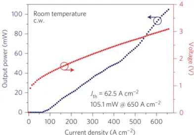
As compared to commercial QW lasers, QD transmitters are much better candidates to reduce the power consumption both of the electrical pumping and the thermoelectric cooling in butterfly-packaged devices [39]. In the current market, mature commercialized GaAs-based QD laser products are already provided for telecommunication applications by different companies such as QD Laser Inc. and Innolume GmbH [43], [65]–[67]. In addition, silicon photonics is anticipated to be a disruptive optical technology for communication system applications, such as intra-chip or inter-chip interconnects [68], short reach communications in datacenters [69] and supercomputers [70], as well as all-optical signal processing [68]. In this context, it was shown that QD lasers display a lower sensitivity to the crystalline defects than QW ones due to the carrier localization and reduced interaction with defects [22], hence constituting better source candidates for silicon integration like in photonics integrated circuits (PICs) [22]. For instance, a very recent work by Chen et al. has successfully demonstrated a 5-layer GaAs-based QD laser directly grown by hetero-epitaxy on silicon, as shown in Figure 1.6, a threshold current density of 62.5 A/cm-2 and a high output power up to 100 mW is reported
30
of view, Ranovus Inc. has also recently launched a 200 Gbps QD-laser-based datacenter interconnect platform, and plans to achieve a 400 Gbps one in the future [71].
Figure 1.6. Light-Current-Voltage (LIV) characteristics of an InAs/GaAs QD laser grown by
hetero-epitaxy on silicon, after [25].
3. InP-based QD lasers
The SK growth has been proved to be very efficient for the realization of GaAs-based QD laser devices, with an emitting wavelength in the O-band (1260 – 1360 nm) that is ideal for short-reach communication links. On the other hand, InAs QDs grown on InP substrates can also be used for the realization of quantum confined devices operating in the C-band. The first InAs/InP QD laser was demonstrated in 1998, first with a lasing operation limited to 77 K [72] and then at room temperature [73]. Although the InAs/InP and InAs/GaAs systems share the same material in the dots, they remain quite different from each other, mostly because the lattice mismatch in InAs/InP (3 %) is smaller than that in InAs/GaAs (7 %) [62]. Therefore, the challenge regarding the dot formation on InP substrates is to deal with the lattice mismatch and the complex strain distribution which tends to produce elongated dots, i.e. quantum dash (QDash), a new class of self-assembled nanostructures that exhibits mixed characteristics in between the quantum wire (QWire) and QD [74].
As an example, Figure 1.7 shows the impact of the trimethylindium (TMIn, In(CH3)3) flow
and of the growth temperature on the formation of the InAs nanostructures on InP(001) substrate. At 500 °C, the InAs tends to form in dashes with the increase of the quantity of TMIn
31
flow, as well as decreasing the temperature with TMIn fixed at 13 sccm.
Figure 1.7. The formation of InAs nanostructures on InP (001) as a function of
trimethylindium (TMIn) flow and growth temperature, after [75].
Figure 1.8 illustrates the cross-section scanning electronic microscopy (X-SEM) image of a QDash laser grown by MBE at the National Research Council (NRC) Canada (courtesy of Dr. Philip Poole). The layers from top to bottom are respectively: InGaAs type contact layer, p-type InP, InGaAsP etch stop layer, p-p-type InP spacer, InGaAsP core containing the QDashes near the top of the core, and the n-type InP layer.
Figure 1.8. Cross-section scanning-electron-microscopy (X-SEM) image of an InAs/InP QDash
laser grown by MBE at the National Research Council (NRC) Canada (courtesy of Dr. Philip Poole).
The dashes are strongly anisotropic nanostructures and exhibit electronic properties rather close to QWires [76]. Thus, the fabrication of real InAs/InP QDs requires careful
32
procedures in order to avoid the formation of QDash, e.g. utilizing miscut InP(100) or InP(311)B misoriented substrates [77].
The formation of nanostructures (dashes or dots) on InP(100) substrate strongly depends on the growth conditions and on the thickness of the InAs layer, hence lots of efforts have been devoted to improve the growth with views of enhancing the dot density [78]. By employing chemical beam epitaxy (CBE), Allen et al. reported an InAs/InGaAsP grating coupled external cavity QD lasers with an increased dot density of 3-6×1010 cm-2 and a wavelength
tuning range of 110 nm [79]. On the other hand, using MBE in conjunction with MOCVD p-doped cladding and contact layers, Lelarge et al. has obtained a very high modal gain up to 10.7 cm-1 per layer by stacking six QD dot in the active region [80]. Very recently, using solid
source MBE (SSMBE) technique, the inhomogeneous broadening was substantially reduced down to 26 meV, allowing a modulation bandwidth of 15 GHz and modulation capabilities up to 36 Gbps [81], [82]. Same as GaAs-based QD lasers, InP-based QD lasers can exhibit reduced threshold currents.
Figure 1.9. Chronological progress of the threshold current density per layer for InAs/InP QD
and QDash lasers, after [77].
Figure 1.9 represents the evolution of the threshold current density per layer in both InAs/InP QD and QDash lasers [77]. Although the lowest value of 78 A/cm2 [83] is still higher
33
than in GaAs-based QD (8.8 A/cm2) [63], InAs/InP QD lasers show a similar trend than the one
displayed in Figure 1.4. Overall, although the performance of InAs/InP QD lasers are still far from those reported on GaAs-based substrate, progress has been made over the years towards demonstrating good performance for optical communications [77].
As compared to InP(100) substrate, it has to be noted that high indexed InP(311)B substrates can provide higher nucleation point density, hence strongly reducing the surface migration effects and allowing the formation of more symmetrical QDs in the planar direction. Moreover, a higher dot density with a smaller dispersion in size can also be obtained. For instance, dot density of 2 to 7.5×1010 cm-2 [84], [85], with dot sizes of 3 nm in high and 30 to
50 nm in wide have been reported. Using an InAs/InGaAsP active region, the first InP(311)B based QD laser was obtained including 7 stack layers grown by MBE and with a dot density of 2×1010 cm-2, displaying a lasing operation at 1400 nm and at 77 K [73]. Then, using a double
capped technique, Caroff et al. achieved a significant improvement in the dot density up to 1.1×1011 cm-2 leading to a threshold current density of 23 A/cm2 per layer [86]. One year later,
by optimizing the InAs deposition process, small QDs (~20 nm) with very high density (~1.3×1011 cm-2) have been reported by the same group [87]. Using a strain compensation
technique, Akahane et al. have recently demonstrated an InP(311)B-based QD laser with 20 QD stacks in the active region, and a high characteristic temperature T0 of 148 K at 298 K [88].
Unfortunately, applications of InAs/InP(311)B QD lasers are still limited since the fabrication requires a more complex technological process that is not always compatible with the industrial standards.
In the following, we will be concentrated on the InAs/GaAs and InAs/InP QD materials, other configurations such as InP/GaP [89], (In, Ga)As/GaP [90], [91] are beyond the scope of this thesis.
III. Motivations of the dissertation
As aforementioned, the recent evolution of optical communication systems is such that the transfer of massive amounts of information is no longer limited to long-distance transoceanic links or backbone networks. Numerous short-reach applications requiring high
34
data throughputs are emerging, not only in access networks, where upgrades of the bit rate of fiber-to-the-home systems need to be anticipated, but also in data center networks where huge amounts of information may need to be exchanged between servers, in part triggered by the rise of “Big Data” applications. In the future, high throughput interconnects will also be required within servers. However, the technological solutions developed over the years for long-distance and high-capacity systems are ill-suited for those emerging applications. The use of direct modulation in telecommunication core networks has been ruled out since the 1990’s when systems have been upgraded to 2.5 Gbps or 10 Gbps operation. The new requirements in terms of cost and energy consumption set by novel short-reach applications therefore need to be considered in the design and operation of a new generation of semiconductor laser sources, which is the main topic of the present dissertation. The evolution of the requirements on new optical transmitters takes two forms. First, energy efficiency has recently become a major concern in the tele- and data-communication world. With a global energy consumption already accounting for more than 2% of the world total and rapidly rising, information and communication technology must take drastic measures to improve the efficiency of its infrastructure. This is precisely one of the targets of using QD lasers. Besides, exploiting the nonlinear properties of QDs is the central point of the thesis with the view of developing novel optical functionalities like all-optical wavelength-converters with improved efficiency as well as optical feedback-resistant transmitters. This last point is even more critical since it is expected that short-reach links making use of directly modulated sources will experience massive deployment in the near future, in contrast to conventional backbone links where the number of required optoelectronic interfaces remains relatively modest. Regarding the long-haul applications, we have seen that the massive deployment of coherent systems does require the implementation of optical sources with narrow linewidth otherwise the sensitivity to the phase noise of both transmitters and local oscillators can strongly affect the bit error rates at the receiver. This is another objective to be addressed in the thesis where, we believe that the opportunities offered by the QD technology may be able to address this challenge. The experimental demonstration of the benefits of QD lasers in the context of the foreseen applications would therefore have a major impact.
35
1. Narrow linewidth QD lasers for coherent communications
The combination of advanced modulation formats and coherent detection are the key technologies in coherent communication systems to overcome the limitations in capacity of the currently fiber infrastructure by increasing the spectral efficiency [92]. Over the past years, the DSP technology has been successfully implemented in the fiber transmission system, in particular, coherent detection can benefit from these novel abilities: the electronic distortion equalization can effectively compensate the impairments over the transmission, and carrier synchronization can be performed by digital phase estimation, thus the optical phase locked loop can be removed and free running lasers can be directly used as local oscillators [92]. However, for high-order modulations, narrow linewidth lasers are still demanded for coherent detection. As an example, for 16-ary quadrature amplitude modulation (16QAM), a 120 kHz linewidth is necessary to ensure a maximal receiver sensitivity with a power penalty less than 2 dB at a 10-4 bit-error rate [92]. Aside from the linewidth, the laser devices must be
single-frequency, low cost and low power consumption. To further reduce the cost and power consumption, future candidate will consider hybrid III-V/Silicon technology where devices can be monolithically integrated on one single chip [93]. QD lasers are promising candidates for coherent communication systems, as previously discussed, they fulfill all these criteria: narrow spectral linewidth, low cost, low power consumption, and suitable for monolithic integration. Theoretically, narrow linewidth from a free-running laser can be obtained at high output power, however, the minimum achievable linewidth is limited by the rebroadening effect due to thermal and nonlinear effects [13], [94]–[98]. Nevertheless, the output power from the local oscillator is crucial in the coherent detection, thus the nonlinear effects must be reduced to achieve a narrow spectral linewidth and a high power lasing operation. In this work, results will show that QD DFB lasers with an optimized design can display a narrow spectral linewidth compatible for coherent systems.
2. QD lasers-based optical wavelength converters
All-optical wavelength converters are the building block for optical signal processing, such
36
wavelength conversion technique, which has the great advantage to be transparent to both,
intensity- and phase-modulated signals [99]–[101]. From a general viewpoint, the
wave-mixing has been widely exploited in wavelength-division multiplexing (WDM) based systems [102] as well as for negative frequency chirping, fiber dispersion compensation [103], [104], optical nonlinear distortion compensation [105] and all-optical signal processing [106], [107]. With the emergence of commercial coherent systems, efficient FWM-based SOA wavelength converters are envisioned for advanced modulation format signals with wideband wavelength conversion over the whole C-band [72],[75]. Most published works have shown that FWM can be generated within different nonlinear media such as nonlinear silica and photonic crystal fibers [108], [109], silicon based micro-rings [110]–[112], and semiconductor optical amplifiers (SOAs) [113], [114]. Although the use of highly nonlinear optical fibers allows very efficient conversion, it usually requires an interaction length of several meters and a large pump power, which are not suitable for monolithic integration. Another important issue with optical fibers is that the required fiber length combined with an operation away from the zero-dispersion wavelength strongly affects the wave mixing and can alter conversion efficiency. On the other hand, recent works have reported efficient FWM with relatively low power consumption in micro-ring resonators. However such resonators usually require sophisticated low-loss bus waveguides design, and fabrication costs may thus be an issue as compared to a simple SOA. In the latter, FWM is obtained from the beating between the incident pump and probe beams and phase-matching is ensured owing to the hetero-structure confinement. Additional
nonlinear effects occurring in SOAs like cross-gain modulation (XGM), and cross-phase
modulation (XPM) can be used for optical wavelength conversion, however these do not
usually provide the same modulation format transparency as does FWM [115].
In forward biased semiconductor devices, the wave mixing is essentially piloted by the carrier density pulsation (CDP) that enhances the static conversion, but with a slow response speed inherently limited by the carrier recombination lifetime (nanosecond timescale) [116]. In contrast, carrier heating (CH) and spectral hole burning (SHB), occurring within picosecond timescales, allow pushing the dynamic frequency conversion over much larger bandwidths, enabling conversion of high rate modulated signals. Although both SHB and CH contribute to increase the bandwidth, their efficiency is also reduced with respect to CDP meaning that a
37
tradeoff between efficiency and bandwidth is to be considered. Another detrimental effect that must be avoided for practical applications is the asymmetry of the conversion efficiency i.e. between up- and down-converted signals [103], [117].For instance, it has been shown that a symmetric conversion allows to convert 40 Gbps non-return-to-zero (NRZ) modulated signal with similar BER penalties in up- and down-conversion in QD SOAs [118]. In this context, QDs constitute a class of nanostructures exhibiting larger optical nonlinearities with faster response speed [117], [119], [120]. As compared to bulk/QW semiconductors, the QD gain material exhibits a spectrally broader and improved conversion efficiency due to faster carrier dynamic and a lower linewidth broadening factor (αH-factor) [117]. Up to now, experimental
studies have mainly focused on QD SOAs, taking advantage of their large linear gain and long interaction length [113], [114], [121], [122]. Instead, this thesis aims at investigating the capabilities of QD oscillators for FWM generation. Taking advantage of both the cavity resonances and reduced amplified spontaneous emission (ASE) noise [123], QD lasers can produce efficient FWM with improved amplitude and bandwidth, and more compact dimensions. In order to further compress the ASE noise, QD lasers using optical-injection-locking (OIL) are considered as originally reported for InGaAs/InP DFB QW lasers [124], [125]. In the dissertation, it will be shown that under proper OIL conditions, nonlinear dynamic of QD lasers allow faster modulation of the converted signals. In this context, an exhaustive comparison between InAs/GaAs and InAs/InP OIL lasers with either QD or QDash nanostructures will be performed. At the end, key-parameters ruling out the conversion performances will be proposed as manufacturing guidelines for future QD-based all-optical wavelength converters.
3. Feedback resistant QD lasers
In order to meet the requirements of the explosive growth in data traffic, fast and low-cost transmitters with low energy consumption are required [5], [126]. Commonly, QD lasers are engineered to operate on the ground-state (GS) transition because of its low threshold current density. In addition, because of the strong damping of the relaxation oscillations, it is also known that QD lasers operating on the GS transition exhibit a larger resistance to external optical feedback which is of primal importance for isolator-free applications i.e. without the
![Figure 2.2. Schematic of a QD laser electronic structure with electrons and holes, after [147]](https://thumb-eu.123doks.com/thumbv2/123doknet/2963464.81711/46.892.285.604.441.779/figure-schematic-qd-laser-electronic-structure-electrons-holes.webp)