HAL Id: hal-00833554
https://hal.archives-ouvertes.fr/hal-00833554
Submitted on 13 Jun 2013
HAL is a multi-disciplinary open access
archive for the deposit and dissemination of
sci-entific research documents, whether they are
pub-lished or not. The documents may come from
teaching and research institutions in France or
abroad, or from public or private research centers.
L’archive ouverte pluridisciplinaire HAL, est
destinée au dépôt et à la diffusion de documents
scientifiques de niveau recherche, publiés ou non,
émanant des établissements d’enseignement et de
recherche français ou étrangers, des laboratoires
publics ou privés.
An FPGA Software Defined Radio Platform with a
High-Level Synthesis Design Flow
Vaibhav Bhatnagar, Ganda Stephane Ouedraogo, Matthieu Gautier, Arnaud
Carer, Olivier Sentieys
To cite this version:
Vaibhav Bhatnagar, Ganda Stephane Ouedraogo, Matthieu Gautier, Arnaud Carer, Olivier Sentieys.
An FPGA Software Defined Radio Platform with a High-Level Synthesis Design Flow. IEEE
In-ternational Vehicular Technology conference (VTC-Spring13), Jun 2013, Dresden, Germany. pp.12.
�hal-00833554�
An FPGA Software Defined Radio Platform
with a High-Level Synthesis Design Flow
Vaibhav Bhatnagar, Ganda Stephane Ouedraogo, Matthieu Gautier, Arnaud Carer and Olivier Sentieys
IRISA, INRIA, Université of Rennes 1, France [email protected]
Abstract— Software defined radio (SDR) opens a new door
to future Internet of Things with higher degree of designing flexibility in context of wireless system development. Prototyping a remote implementation of wireless protocols on a hardware over the web requires a highly versatile software radio platform along with laid-back designing tools.
To this aim, an FPGA-based SDR scheme has been proposed combining Virtex-6 Perseus 6010 platform capabilities and a design flow based on High-Level Synthesis (HLS) tools. A full IEEE 802.15.4 (ZigBee) physical layer has been implemented on the proposed platform from a C-language dataflow specification. All the results have been analyzed to lead to a fair comparison between different design flows. Although the proposed SDR has some designing issues, it shows a noticeable designing potentiality to flexible prototyping of future wireless systems.
Index Terms— Flexible Software Defined Radio, High-Level
Synthesis, FPGA platform.
I. INTRODUCTION
The Software Defined Radio (SDR) was an early idea of Joseph Mitola, in which he proposed a reconfigurable hardware on software level by using a host-PC design [1]. This implies the possibility of changing coding scheme, mod-ulation, bandwidth and channel access technique in a software without modifying the hardware [2].
The Future Internet of Things (FIT) project [3] aims to develop a novel infrastructure offering a means to experiment on mobile wireless communications, thereby accelerating the design of advanced technologies. In the context of FIT, the development of FPGA-based SDR can be accelerated by the design approach where a user of any domain can implement and test its design remotely on an FPGA-based hardware over the web.
The two fundamental keys to achieve this goal of a fully flexible physical layer are [4]: a specific development method-ology allowing the flexibility of high-level specifications and a modular architecture supporting various waveforms. In this paper, an FPGA-based SDR platform is developed using High-Level Synthesis (HLS) design flow [5]. It associates the flexibility of high-level specifications with the efficiency of FPGA implementation.
The proposed design methodology is based on high-level specifications which allows to manage all the waveform’s parameters at a system level [4][6]. HLS flow is used to develop signal processing blocks at the algorithmic level in the FPGA platform of the waveform previously described. It
provides a significant gain in term of productivity, flexibility, parameterization and reusability. Catapult C synthesis [7] from Calypto Design Systems is used in this study.
There are many FPGA-based platforms that have already been developed for implementing wireless communication stack. A comparison has already been made in [8][9]. The well-known GNU radio/USRP is a low-cost radio platform where the signal processing takes place in host-PC using signal processing primitive blocks implemented in C++. The WARP platform supports low-level VHDL/Verilog coding to Matlab Simulink modeling [9], however the radio boards cover only 2.4 GHz and 5 GHz ISM bands and the old Virtex-4 FPGA is used.
Thus, willing at proposing a design flow from high-level specifications to FPGA bitstream generation, we emphasize on Nutaq Perseus 6010 [10]. Perseus 6010 hardware has high flexibility of wireless radio and protocol designs to fulfill all the recent requirements of optimal utilization of FPGA resources in design. In comparison of all existing platforms, it utilizes less power using the latest low power Xilinx Virtex-6 FPGA, it addresses much radio frequency bands and it has facility to work stand-alone with all physical-layer signal processing design working on its FPGA.
As a study case, the IEEE 802.15.4 (ZigBee) physical layer has been successfully designed using both hand-coded VHDL and HLS tool and implemented on Perseus 6010. Both transmitter and receiver have been successfully designed, and FPGA resources have been estimated for different designs. The rest of the paper is organized as follows: Section II describes the proposed SDR design flow as well as the Perseus 6010 hardware. The IEEE 802.15.4 implementation on Perseus 6010 is detailed in Section III. Section IV enlightens the comparison of different designing methodologies, and Section V presents some recorded results and FPGA resource estimation. Finally, Section VI gives the conclusion and future works.
II. DESCRIPTION OFSDRDESIGN FLOWS
Starting from high-level specifications of the radio wave-form, we propose to describe, test and compare different ways to implement a design on an FPGA based platform.
The first step of the design flow is to describe the algo-rithm/waveform using high-level description language.
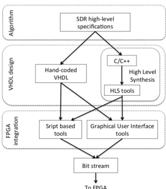
Well-Fig. 1: SDR design flows.
known language (C/C++, Matlab,. . . ) as well as specific
dedicated language could here be used.
The second step is to generate a VHDL code that performs the specified waveform. Two ways are tested in this paper: the code can be hand-coded (HC) or it can results from a HLS tool (HLS-VHDL). HLS integration in the design flow provides a flexibility of including high-level languages (C/C++) in design. The third step is to integrate the design on the FPGA platform. This step depends on the platform and the associated tools. However, an FPGA platform design flow most often includes a graphical user interface (GUI) tools and/or VHDL script-based tools. For example, an FPGA design can be implemented on Xilinx ML605 evaluation kit by using the GUI tool Simulink or using the VHDL script based tool Xilinx Platform Studio (XPS) [11].
Fig. 1 introduces the design flows that is proposed and tested in the paper. Four ways are described:
• HC-VHDL integration in design using script based tools,
• HC-VHDL integration in design using GUI tools,
• HLS-VHDL integration in design using script based tools,
• HLS-VHDL integration in design using GUI tools.
The first flow is the only full VHDL integration flow, the others use either GUI tool or HLS tool or both.
In our study, the HLS tool that has been used is Catapult C synthesis [7] provided by Calypto Design Systems. For the integration of the radio physical layer, Xilinx FPGA Virtex-6 based Nutaq Perseus 6010 has been selected as a target platform.
The Perseus 6010 is intended for performance, high-bandwidth, low-latency processing applications. It is an ad-vanced mezzanine card, which is designed around the
pow-bit to symbol symbol to chip serial to parallel 2 Mchip/s 1 Mchip/s 1 Mchip/s NRZ 8 MHz delay end Front Rado420x pulse shapping 1 Mchip/s 1 Mchip/s 8 MHz Front end Rado420x Reverse pulse shapping delay Down Conver. parallel to serial 8 MHz 8 MHz 62.5 symbols/s Synchro 2 Mchip/s bit to symbol 62.5 ksymbols/s Bit stream 250 kbps 250 kbps
Bit stream Corr Bench and Decision
1 Mchip/s
Rx Filter Chip Gen Tx Filter
1 Mchip/s
Receiver Transmitter
Fig. 2: Block diagram of IEEE 802.15.4 transceiver.
erful Virtex-6 FPGA, combining fabric flexibility and a huge external memory, as well as benefiting from multiple high-pin-count, modular, add-on FPGA mezzanine card (FMC)-based cards.
In our testbed, the Radio 420x FMC card [10] is used as a full duplex multimode SDR RF transceiver with 12 bits and 40 MBPS baseband conversion capability. Thus, the testbed is compatible with a huge variety of physical layers by modifying the modulation scheme, the baseband bandwidth and the RF frequency.
In context of Fig. 1, Nutaq Perseus 6010 can be designed by using Model Based Design Kit (MBDK), a GUI (Simulink) based tool or by using Board Software Development Kit (BSDK), the VHDL/Verilog script based development of any Xilinx FPGA based platforms (designed with Xilinx Integrated Software Environment (ISE) [12]).
III. IEEE 802.15.4IMPLEMENTATION ONPERSEUS6010
This section introduces the IEEE 802.15.4 physical layer and its designed and implemention on Perseus 6010 by fol-lowing the presented design flows in Section II.
A. IEEE 802.15.4 physical layer description
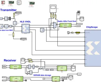
The multirate block diagram of IEEE 802.15.4 transmitter and receiver can be seen in Fig. 2. At the transmitter side, a binary raw data at the basic rate of 250 kbps has been given to the bit-to-symbol block, which converts this data in to 4-bit symbol and further supply it to symbol to chip block at rate 62.5 ksymbols/s. Thereafter, each symbol is spread into a 32-chip pseudo-sequence at rate of 2 M32-chip/s and is forwarded to a serial to parallel block, which produces 16-bit I and Q signals at half rate. The pulse shaping block up-converted the 1 Mchip/s I and Q signals to 8 MHz with an half-sine pulse shaping. Finally, a delay is inserted to Q chip before going to front-end for transmission [13] in order to satisfy the offset of Offset-Quadrature Phase Shift Keying (O-QPSK) modulation [14].
At the receiver side, the baseband is extracted by the front-end and supplied to the matched filtering block, where extracted 8 MHz data are converted to 1 Mchip/s I and Q chips with
Raw data from MAC
RECEIVER SECTION TRANSMITTER SECTION
Chip Gen Tx Filter
Sample Delay Radio 420x Front End
Radio 420x Front End
Rx Filter Sample Delay Synchro Parallel to Serial Decision Block SDRAM Storage Chipscope sdram memory to host SDRAM MemToHost rtdex_ready rtdex_data rtdex_we rtdex RTDEx TX:Ch0 GIGe 0 data txEn ready Terminator6 Terminator5 Terminator4 Terminator3 Terminator Synchro reset ich4 qch4 delay Step1 Scope5 Scope3 Scope RTDEx Sample_Delay_I reset data_in data_out Rx_Filter reset ich3 qch3 ich4 qch4 Rising Edge Detector1 Din Dout Resource Estimator Reset Generator1 rst rst5 rst2 rdy Reset Generator rst rst5 rst2 rdy Register d en q z−1 Register d en q z−1 Radio420X2 Radio420S ADC− ch1 data adc_IQ_sel Radio420X Radio420S DAC− ch1 data dac_IQ_sel ROM addrz−4 Q_Tx reset data sample_out Mux sel d0 d1 Inverter not I_Tx reset data sample_out [dac_iq_sel] [dac_data] [rtdex_tx_rdy]
Gateway Out31 Out Gateway Out27 Out
Out Gateway Out16 Out Gateway Out15 Out Gateway Out11 Out Gateway Out Out Out [datarecord] [dac_data] [rtdex_tx_rdy] [dac_iq_sel] FPGA board configuration FPGA Perseus 601x z−1 ↓2 z−1 ↓2 Display Delay z−1 Delay reset data_in data_out Decision Block reset delay ich5 qch5 chip_out int32 Counter2 ++ Counter ++ Corr_Bench reset Chip Valid_out Symbol cast cast Convert2 cast cast Convert cast 1 1 Constant4 1 Constant3 1 trig0_low_to_high data0 data1 data2 data3 data4 data5 data6 data7 ChipGen reset symbol ich qch Center_PB_SW In System Generator trig0_low_to_high
Fig. 3: IEEE 802.15.4 transmitter MBDK HC-VHDL devel-opment.
proper synchronization and down conversion. Thereafter, I and Q chips are converted in serial data at 2 Mchip/s and forwarded to correlation bench block that performs sliding correlations with all the 16 spreading codes. Finally, a threshold-based decision is made-up to recover the transmitted symbols.
B. MBDK integration flow
MBDK is a Matlab Simulink model based GUI design kit, which uses Xilinx system generator to generate a low-level FPGA design [10]. The system generator utilizes the Xilinx tools to compile the simulink model and generate the bitstream that will be implemented in the hardware.
With MBDK, a design can be developed with the help of specific Xilinx and Nutaq’s blockset integrated in a Simulink library. The HC-VHDL or HLS-VHDL can be integrated in the design by using Xilinx black box utility [12].
The IEEE 802.15.4 transceiver has been designed in MBDK with the integration of HC-VHDL (Fig. 3) and HLS-VHDL (Fig. 4). Both figures represent the multirate MBDK model in simulink environment that corresponds to Fig. 2. Fig. 3 shows that the HC-VHDL code has been splitted into several black boxes corresponding to the different blocks in Fig. 2. For the HLS-VHDL, the connection of the different blocks has been previously performed in VHDL in such a manner that only one black box is used in the MBDK model (see Fig. 4). Both the models include IEEE 802.15.4 baseband design as well as the Nutaq Radio 420x front-end block. It is good to notify that the Radio 420x block is an inactive block in the MBDK model because practically it is not part of FPGA. But at the time of bitstream generation, this block tells system generator about the connections of FPGA design with it. So, it is necessary to have this block in the design to generate a fully working design which includes the Radio 420x front-end in the design flow.
Raw data from MAC
Radio 420x Front End HLS VHDL
Transmitter
Receiver
ChipScope
SDRAM data storage
sdram record SDRAM Record data_ch0 data_ch1 wen sdram memory to host SDRAM MemToHost rtdex_ready rtdex_data rtdex_we rtdex RTDEx TX:Ch0 GIGe 0 data txEn ready To Workspace simout Step1 Spectrum Scope2 B−FFT Scope3 Scope2 Scope1 Scope RTDEx Scope Rising Edge Detector1 Din Dout Reset Generator rst rst5 rst2 rdy Register d en q z−1 Register d en q z−1 Radio420X2 Radio420S ADC− ch1 data adc_IQ_sel Radio420X Radio420S DAC− ch1 data dac_IQ_sel ROM addr z−4 Mux sel d0 d1 ModelSim ModelSim Inverter1 not Inverter not Host board configuration Host Perseus 601x [dac_iq_sel] [dac_data] [rtdex_tx_rdy] Gateway Out9 Out Gateway Out8 Out Gateway Out3 Out Out Out Gateway Out1 Out Out [dac_data] [dac_data] [rtdex_tx_rdy] [dac_iq_sel] FPGA board configuration FPGA Perseus 601x z−1 ↓2 z−1 ↓2 z−1 ↓2 Display1 Display Delay z−1 int32 Counter2 ++ Counter1 ++ Convert cast 1 1 Constant3 1 CEProbe trig0_low_to_high data0 data1 data2 data3 data4 data5 data6 Center_PB_SW In Black Box rst data ich qch ich_r qch_r System Generator trig0_low_to_high
Fig. 4: IEEE 802.15.4 transmitter MBDK HLS-VHDL devel-opment.
C. BSDK integration flow
BSDK is a script based low-level design kit, which uses XPS as an entry point [10]. In XPS [12], it may use a VHDL description in FPGA design by creating a user-defined intellectual property (IP) block. An IP block is a small FPGA design, which behaves as a defined VHDL script. It has a high degree of designing flexibility due to low-level programming inclusion.
In BSDK, after downloading the HC/HLS-VHDL designs on the FPGA in the form of a bitstream, one may need a software script in C to read/write raw data from MAC layer to physical layer. This C script is used by MicroBlaze for the reading and writing operations over the logical bus to and from the IP inside FPGA. Basically MicroBlaze is a soft core processor that provides a highly flexible architecture with an instruction set optimized for embedded applications, delivering the exact processing system you need at the lowest system cost possible. Although BSDK has many features, it has a higher designing complexity because of the custom IP creation. Moreover, in MBDK a separate MicroBlaze C script is not needed, which makes a difference with BSDK. In MBDK, system generator is responsible for an auto excited MicroBlaze, once the bitstream is loaded to FPGA.
IV. DESIGN FLOW COMPARISON
The main difference in design can be stated on the basis of VHDL scripts, which can be either hand-coded or using HLS. These two types of VHDL design can be implemented on the FPGA platform by using MBDK or BSDK. However both tools are different in terms of complexity and have different features as described below.
A. Hand-coded versus High-Level Synthesis
Both VHDL are generated in different ways: HC-VHDL is directly written by a user corresponding to a design while HLS-VHDL comes from Catapult C Synthesis (from a C/C++
Fig. 5: Working test bench Perseus.
language design).
In terms of design complexity, HLS-VHDL is machine gen-erated hence the code is hard to understand in comparison of HC-VHDL. But in terms of system complexity HLS provides a straight forward optimized FPGA design in comparison of HC-VHDL. By comparing both HC-VHDL and HLS-VHDL designs, it can be stated that HLS-VHDL design uses less FPGA resources than HC-VHDL (see Table I in Section V). Our experience feedback is that the HLS design reduces the hardware resource as well as the development time. Actually, the main advantage of HLS is the development time that has been drasticly reduced and the simplicity of C coding and validation in the context of SDR physical layer development.
B. MBDK tools versus BSDK tools
Xilinx system generator is a key component of MBDK design kit, it provides many features such as resource estimator or hardware co-simulation. The designing is quite straight forward as a drag-and-drop due to Simulink GUI, but it uses lots of computer resources to compile and run the program. FPGA design is restricted due to available Xilinx blocksets in Simulink library hence for extending the design, Xilinx black box can be helpful, but it may encounter some VHDL integration problem.
On the other hand, BSDK is a low-level designing approach, which uses less computer resources in order to mitigate a wrong generation of bitstream. However a BSDK designing needs a good understanding of Xilinx tools and VHDL pro-gramming. BSDK design has a full flexibility of designing due to inclusion of custom IP. Moreover, BSDK design in XPS can also be included to ISE software, which provides a full summary on the FPGA design like resource estimation. Our experience feedback is that if a user has less understanding of hardware, it may go for easy MBDK tool to test its design. On the other hand, if a user has a good knowledge of Xilinx tools and VHDL, it may go for full VHDL integration (BSDK).
V. INTEGRATION RESULTS OFIEEE 802.15.4ONPERSEUS
6010PLATFORM
The Nutaq Perseus 6010 testbed has been developed
suc-cessfully with twoµTCA chassis as illustrated in Fig. 5: one
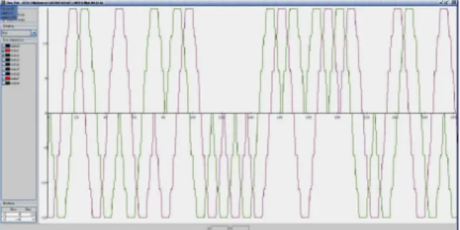
Fig. 6: Transmitted baseband signals in Chip-scope MBDK: HLS-VHDL.
Fig. 7: Received baseband signals in Chip-scope MBDK: HLS-VHDL.
for the transmitter and one for the receiver.
The IEEE 802.15.4 transmitter has been designed and im-plemented by using MBDK designing tool in Simulink and also by using BSDK by XPS. As the MBDK and BSDK tools propose two different manners for FPGA integration, they obviously lead to the same results in terms of generated waveform. Thus, only MBDK results are introduced in the following.
The MBDK Simulink design has been developed with the in-tegration of both HC-VHDL (Fig. 3) and HLS-VHDL (Fig. 4). The system clock has been reduced to 16 MHz to achieve a low power FPGA design. As comparison criteria, waveforms and spectrums have been observed for the two designs and resource estimations have been analyzed on FPGA design level. The waveforms have been captured from FPGA model using Xilinx ChipScope [12]. Transmit baseband signals of 8 MHz each can be observed in Fig. 6 for the HLS-VHDL design, it shows the standard I and Q signals after pulse shaping. At the receiver side, the extracted signals from receiver matched filter after the Radio 420x front-end can be seen in Fig. 7. Waveforms in Fig. 6 and Fig. 7 are generated using HLS-VHDL design, similar waveforms have been observed for HC-VHDL (not shown in the paper).
The modulated spectrum can be visualized in a spectrum analyzer as shown in Fig. 8. The spectrum is compared with a IEEE 802.15.4 reference spectrum in Fig. 9, spectrum generated by the CC2420 component [15]. These figures show that our design leads to a similar 3.5 MHz band as the commercial component.
Fig. 8: Modulated spectrum MBDK: HLS-VHDL.
Fig. 9: Reference spectrum: CC2420.
Finally, resource estimations have been performed to compare the HC-VHDL and the HLS-VHDL designs of the transmitter. Results are introduced in Table I. The two designs lead to similar resources. Furthermore, the HLS compiler proposes optimization tools that have not been used in this study.
VI. CONCLUSION
To meet the flexibility and the high-level of specifications required by new SDR waveforms, it is mandatory to introduce innovative high-level design approaches such as using C-based specifications and HLS tools. In this work, we have provided a concrete study of different design methodologies allowing the integration of a physical layer with high-level specifications
Slices FF BRAM LUT IOB
HC-VHDL 35 134 0 86 18
HLS-VHDL 76 188 0 202 16
TABLE I: Resource estimation of IEEE 802.15.4 transmitter designs.
on the Nutaq Perseus 6010 platform. All high-level and low-level integrations have been studied in a good order to make a fair comparison about designing potentiality towards FIT framework.
The complete design and implementation of the IEEE 802.15.4 transmitter strengthen the proposed design flow.
Only a single waveform has been developed in this paper, the methodology should be extended to the design of several waveforms in order to address flexibility. A solution is to defined a specific waveform description language that fits with the proposed design flow.
ACKNOWLEDGMENT
The research leading to these results was
derived from the project Future Internet of Things
(http://fit-equipex.fr), one of 52 winning projects from the French Ministry of Higher Education and Research’s
"Equipements d’Excellence" (Equipex) research grant
programme.
REFERENCES
[1] J. Mitola III, “Software radios : Survey, critical evaluation and future directions,” Aerospace and Electronic systems Magazine, IEEE, vol. 8, 1993.
[2] A. Di Stefano, G. Fiscelli, and C. Gianconia, “An FPGA-Based Software Defined Radio Platform for the 2.4GHz ISM Band,” in IEEE PRIME
2006. IEEE Ph. D. Research in Microelectronics and Electronics,
vol. 12, 2006, pp. 73–76.
[3] FIT project: Future Internet of Things. [Online]. Available: http: //fit-equipex.fr/
[4] F. Kasperski, O. Pierrelee, F. Dotto, and M. Sarlotte, “High data rate fully flexible sdr modem,” in Design, Automation Test in Europe Conference
Exhibition, 2009. DATE ’09., april 2009, pp. 1040 –1044.
[5] J. Cong, B. Liu, S. Neuendorffer, J. Noguera, K. Vissers, and Z. Zhang, “High-Level Synthesis for FPGAs: From Prototyping to Deployment,”
IEEE Transactions on Computer-Aided Design of Integrated Circuits and Systems, vol. 30, no. 4, pp. 473 –491, april 2011.
[6] M. Rossler, H. Wang, U. Heinkel, N. Engin, and W. Drescher, “Rapid prototyping of a dvb-sh turbo decoder using high-level-synthesis,” in
Specification Design Languages, 2009. FDL 2009. Forum on, sept. 2009,
pp. 1 –6.
[7] T. Bollaert, High-Level Synthesis: From Algorithm to Digital Circuit. Springer, 2008, ch. Catapult synthesis: a practical introduction to inter-active C synthesis, pp. 29–52.
[8] O. Gustafsson and al., “Architectures for cognitive radio testbeds and demonstrators - an overview,” in IEEE Cognitive Radio Oriented
Wire-less Networks & Communications (CROWNCOM’10), 2010, pp. 1–6.
[9] M. Dardaillon, K. Marquet, T. Risset, and A. Scherrer, “Software defined radio architecture survey for cognitive testbeds,” in Wireless
Communications and Mobile Computing Conference (IWCMC), 2012 8th International, aug. 2012, pp. 189 –194.
[10] Nutaq, Nutaq Perseus 601X User’s guide. [Online]. Available: http://nutaq.com/en/products/view/+nutaq-perseus-601x#Downloads [11] Xilinx, Virtex-6 FPGA ML605 Evaluation Kit. [Online]. Available:
http://www.xilinx.com/products/boards-and-kits/EK-V6-ML605-G.htm [12] ——, ISE 12.1 documents and tools. [Online]. Available: http:
//www.xilinx.com/products/design-tools/ise-design-suite/index.htm [13] C. Bernier, F. Hameau, G. Billiot, E. de Foucauld, S. Robinet, D. Lattart,
J. Durupt, F. Dehmas, L. Ouvry, and P. Vincent, “An ultra low power soc for 2.4ghz ieee 802.15.4 wireless communications,” in European
conference on Public Key Infrastructures, Services, and Applications (EuroPKI’11), 2011, pp. 194–208.
[14] IEEE Computer Society, Part 15.4: Wireless Medium Access Control
(MAC) and Physical Layer (PHY) Specifications for Low-Rate Wireless Personal Area Networks (WPANs). [Online]. Available:
http://www.ieee802.org/15/pub/TG4.html
[15] Texas Instrumentation, CC2420 TI data sheet. [Online]. Available: www.ti.com/lit/ds/symlink/cc2420.pdf